Analog Devices AD8017 c Datasheet

Dual High Output Current,
+V
S
R1
+
–
–V
S
R2
N
P:NS
TRANSFORMER
V
IN
V
REF
V
OUT
LINE
POWER
IN dB
+
–
R
L
= 100⍀
OR
135⍀
a
FEATURES
High Output Drive Capability
20 V p-p Differential Output Voltage, R
10 V p-p Single-Ended Output Voltage While
Delivering 200 mA to a 25 ⍀ Load
Low Power Operation
5 V to 12 V Voltage Supply @ 7 mA/Amplifier
Low Distortion
–78 dBc @ 500 kHz SFDR, R
–58 dBc Highest Harmonic @ 1 MHz, I
= 10 ⍀)
(R
L
High Speed
160 MHz, –3 dB Bandwidth (G = +2)
1600 V/s Slew Rate
APPLICATIONS
xDSL PCI Cards
Consumer DSL Modems
Line Driver
Video Distribution
= 100 ⍀, VO = 2 V p-p
L
= 50 ⍀
L
= 270 mA
O
High Speed Amplifier
AD8017
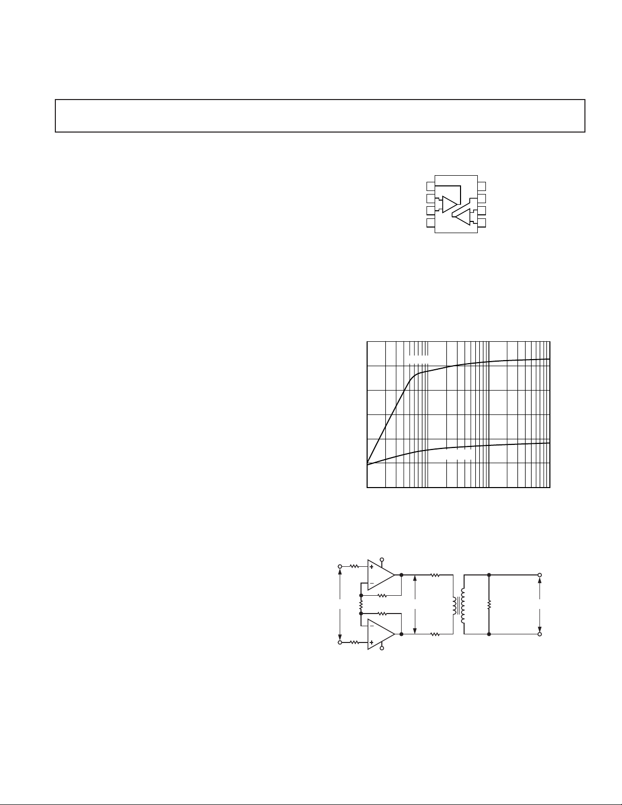
PIN CONFIGURATION
8-Lead Thermal Coastline SOIC (SO-8)
AD8017
1
OUT1
2
–IN1
+IN1
12
10
VS = ⴞ6V
–
+
3
–V
4
S
8
+V
S
7
OUT2
6
–IN2
–
+
5
+IN2
8
6
PRODUCT DESCRIPTION
The AD8017 is a low cost, dual high speed amplifier capable of
driving low distortion signals to within 1.0 V of the supply rail.
It is intended for use in single supply xDSL systems where low
distortion and low cost are essential. The amplifiers will be able
to drive a minimum of 200 mA of output current per amplifier.
The AD8017 will deliver –78 dBc of SFDR at 500 kHz, required
for many xDSL applications.
Fabricated in ADI’s high speed XFCB process, the high bandwidth
4
OUTPUT VOLTAGE SWING – V p-p
2
0
1
VS = ⴞ2.5V
10010
LOAD RESISTANCE – ⍀
Figure 1. Output Swing vs. Load Resistance
1000
and fast slew rate of the AD8017 keep distortion to a minimum, while
dissipating a minimum amount of power. The quiescent current of
the AD8017 is 7 mA/amplifier.
Low distortion, high output voltage drive, and high output current
drive make the AD8017 ideal for use in low cost Customer Premise
End (CPE) equipment for ADSL, SDSL, VDSL and proprietary
xDSL systems.
The AD8017 drive capability comes in a very compact form.
Utilizing ADI’s proprietary Thermal Coastline SOIC package,
the AD8017’s total (static and dynamic) power on 12 V supplies
is easily dissipated without external heat sink, other than to place
the AD8017 on a 4-layer PCB.
The AD8017 will operate over the commercial temperature
Figure 2. Differential Drive Circuit for xDSL Applications
range –40°C to +85°C.
REV. C
Information furnished by Analog Devices is believed to be accurate and
reliable. However, no responsibility is assumed by Analog Devices for its
use, nor for any infringements of patents or other rights of third parties that
may result from its use. No license is granted by implication or otherwise
under any patent or patent rights of Analog Devices.
One Technology Way, P.O. Box 9106, Norwood, MA 02062-9106, U.S.A.
Tel: 781/329-4700 www.analog.com
Fax: 781/326-8703 © Analog Devices, Inc., 2002

AD8017–SPECIFICATIONS
(@ 25ⴗC, VS = ⴞ6 V, RL = 100 ⍀, RF = RG = 619 ⍀, unless otherwise noted.)
Parameter Conditions Min Typ Max Unit
DYNAMIC PERFORMANCE
–3 dB Bandwidth G = +2, V
0.1 dB Bandwidth V
Large Signal Bandwidth V
< 0.4 V p-p 70 MHz
OUT
= 4 V p-p 105 MHz
OUT
Slew Rate Noninverting, V
Rise and Fall Time Noninverting, V
Settling Time 0.1%, V
< 0.4 V p-p 100 160 MHz
OUT
= 4 V p-p, G = +2 1600 V/µs
OUT
= 2 V p-p 2.0 ns
OUT
= 4 V Step 35 ns
OUT
Overload Recovery VIN = 5 V p-p 74 ns
NOISE/HARMONIC PERFORMANCE
Distortion V
Second Harmonic 500 kHz, R
Third Harmonic 500 kHz, R
IP3 500 kHz, R
IMD 500 kHz, R
= 2 V p-p
OUT
1 MHz, R
1 MHz, R
= 100 Ω/25 Ω –78/–71 dBc
L
= 100 Ω/25 Ω –76/–69 dBc
L
= 100 Ω/25 Ω –105/–91 dBc
L
= 100 Ω/25 Ω –81/–72 dBc
L
= 100 Ω/25 Ω 40/35 dBm
L
= 100 Ω/25 Ω –76/–66 dBc
L
MTPR 26 kHz to 1.1 MHz –66 dBc
Input Noise Voltage f = 10 kHz 1.9 nV/√Hz
Input Noise Current f = 10 kHz (+ Inputs) 23 pA/√Hz
f = 10 kHz (– Inputs) 21 pA/√Hz
Crosstalk f = 5 MHz, G = +2 –66 dB
DC PERFORMANCE
Input Offset Voltage 1.8 3.0 mV
T
Open Loop Transimpedance V
to T
T
MIN
OUT
MIN
MAX
= 2 V p-p 185 700 kΩ
to T
MAX
143 kΩ
4.0 mV
INPUT CHARACTERISTICS
Input Resistance +Input 50 kΩ
Input Capacitance +Input 2.4 pF
Input Bias Current (+) 16 ±45 µA
T
MIN
to T
MAX
±67 µA
Input Bias Current (–) 1.0 ±25 µA
CMRR V
to T
T
MIN
CM
MAX
= ±2.5 V 59 63 dB
±32 µA
Input CM Voltage Range ±5.1 V
OUTPUT CHARACTERISTICS
Output Resistance 0.2 Ω
Output Voltage Swing R
Output Current
1
= 25 Ω±4.6 ±5.0 V
L
Highest Harmonic < –58 dBc, 200 270 mA
f = 1 MHz, R
to T
T
MIN
= 10 Ω
L
, Highest Harmonic < –52 dBc 100 mA
MAX
Short-Circuit Current 1500 mA
POWER SUPPLY
Supply Current/Amp 7.0 7.7 mA
T
MIN
to T
MAX
7.8 mA
Operating Range Dual Supply ± 2.2 ±6.0 V
Power Supply Rejection Ratio 58 61 dB
Operating Temperature Range –40 +85 °C
NOTE
1
Output current is defined here as the highest current load delivered by the output of each amplifier into a specified resistive load ( RL = 10 Ω), while maintaining an
acceptable distortion level (i.e., less than –60 dBc highest harmonic) at a given frequency (f = 1 MHz).
Specifications subject to change without notice.
–2–
REV. C

AD8017
SPECIFICATIONS
Parameter Conditions Min Typ Max Unit
DYNAMIC PERFORMANCE
–3 dB Bandwidth G = +2, V
0.1 dB Bandwidth V
Large Signal Bandwidth V
Slew Rate Noninverting, V
Rise and Fall Time Noninverting, V
Settling Time 0.1%, V
Overload Recovery VIN = 2.5 V p-p 74 ns
NOISE/HARMONIC PERFORMANCE
Distortion V
Second Harmonic 500 kHz, R
Third Harmonic 500 kHz, R
IP3 500 kHz, R
IMD 500 kHz, R
MTPR 26 kHz to 1.1 MHz –66 dBc
Input Noise Voltage f = 10 kHz 1.8 nV/√Hz
Input Noise Current f = 10 kHz (+ Inputs) 23 pA/√Hz
Crosstalk f = 5 MHz, G = +2 –66 dB
DC PERFORMANCE
Input Offset Voltage 0.8 2.0 mV
Open Loop Transimpedance V
INPUT CHARACTERISTICS
Input Resistance +Input 50 kΩ
Input Capacitance +Input 2.4 pF
Input Bias Current (+) 16 ±40 µA
Input Bias Current (–) 2 ±25 µA
CMRR V
Input CM Voltage Range ±1.6 V
OUTPUT CHARACTERISTICS
Output Resistance 0.2 Ω
Output Voltage Swing R
Output Current
Short-Circuit Current 1300 mA
POWER SUPPLY
Supply Current/Amp 6.2 7 mA
Operating Range Dual Supply ±2.2 ±6.0 V
Power Supply Rejection Ratio 59 62 dB
Operating Temperature Range –40 +85 °C
NOTE
1
Output current is defined here as the highest current load delivered by the output of each amplifier into a specified resistive load ( RL = 10 Ω), while maintaining an
acceptable distortion level (i.e., less than –60 dBc highest harmonic) at a given frequency (f = 1 MHz).
Specifications subject to change without notice.
1
(@ 25ⴗC, VS = ⴞ2.5 V, RL = 100 ⍀, RF = RG = 619 ⍀, unless otherwise noted.)
< 0.4 V p-p 75 120 MHz
OUT
< 0.4 V p-p 40 MHz
OUT
= 4 V p-p 100 MHz
OUT
OUT
= 2 V p-p
OUT
1 MHz, R
1 MHz, R
= 2 V Step 35 ns
L
= 100 Ω/25 Ω –73/–66 dBc
L
L
= 100 Ω/25 Ω –79/–74 dBc
L
L
L
= 2 V p-p, G = +2 800 V/µs
OUT
= 2 V p-p 2.2 ns
OUT
= 100 Ω/25 Ω –75/–68 dBc
= 100 Ω/25 Ω –91/–88 dBc
= 100 Ω/25 Ω 40/36 dBm
= 100 Ω/25 Ω –78/–64 dBc
f = 10 kHz (– Inputs) 21 pA/√Hz
T
to T
T
T
T
MIN
OUT
MIN
MIN
MIN
CM
L
MAX
= 2 V p-p 40 166 kΩ
to T
to T
to T
MAX
MAX
MAX
45 kΩ
= ±1.0 (±1.0) 57 60 dB
= 25 Ω±1.55 ±1.65 V
Highest Harmonic < –55 dBc, 100 120 mA
f = 1 MHz, R
T
to T
MIN
to T
T
MIN
= 10 Ω
L
Highest Harmonic < 50 dBc 60 mA
MAX
MAX
2.6 mV
±62 µA
±32 µA
7.3 mA
–3–REV. C

AD8017
WARNING!
ESD SENSITIVE DEVICE
ABSOLUTE MAXIMUM RATINGS
Supply Voltage . . . . . . . . . . . . . . . . . . . . . . . . . . . . . . . . 13.2 V
Internal Power Dissipation
2
1
Small Outline Package (R) . . . . . . . . . . . . . . . . . . . . . . . 1.3 W
Input Voltage (Common Mode) . . . . . . . . . . . . . . . . . . . . ± V
S
Differential Input Voltage . . . . . . . . . . . . . . . . . . . . . . ± 2.5 V
Output Short Circuit Duration
. . . . . . . . . . . . . . . . . . . . Observe Power Derating Curves
Storage Temperature Range . . . . . . . . . . . . –65°C to +125°C
Operating Temperature Range . . . . . . . . . . . –40°C to +85°C
Lead Temperature Range (Soldering 10 sec) . . . . . . . . . 300°C
NOTES
1
Stresses above those listed under Absolute Maximum Ratings may cause perma-
nent damage to the device. This is a stress rating only; functional operation of the
device at these or any other conditions above those indicated in the operational
section of this specification is not implied. Exposure to absolute maximum rating
conditions for extended periods may affect device reliability.
2
Specification is for device on a two-layer board with 2500 mm2 of 2 oz. copper at
+25°C 8-lead SOIC package: θJA = 95.0°C/W.
MAXIMUM POWER DISSIPATION
The maximum power that can be safely dissipated by the AD8017
is limited by the associated rise in junction temperature. The
maximum safe junction temperature for plastic encapsulated
device is determined by the glass transition temperature of the
plastic, approximately 150°C. Temporarily exceeding this limit
may cause a shift in parametric performance due to a change in
the stresses exerted on the die by the package. Exceeding a junction temperature of 175°C for an extended period can result in
device failure.
ORDERING GUIDE
The output stage of the AD8017 is designed for maximum load
current capability. As a result, shorting the output to common
can cause the AD8017 to source or sink 500 mA. To ensure
proper operation, it is necessary to observe the maximum power
derating curves. Direct connection of the output to either power
supply rail can destroy the device.
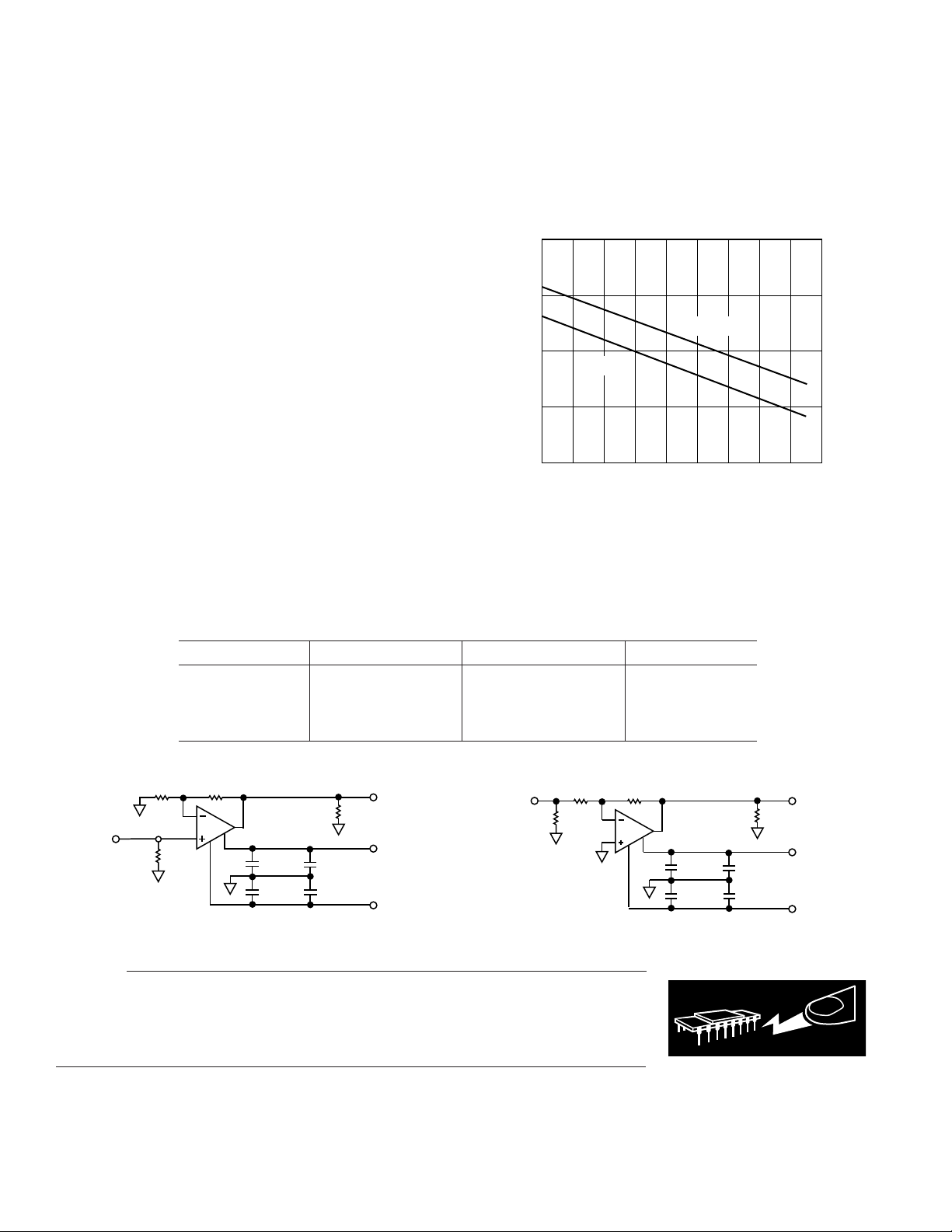
2.0
1.5
TJ = 150ⴗC
1.0
0.5
MAXIMUM POWER DISSIPATION – Watts
0
09010
TJ = 125ⴗC
20 30 40 50 60 70 80
AMBIENT TEMPERATURE – ⴗC
Figure 3. Plot of Maximum Power Dissipation vs.
Temperature for AD8017
Model Temperature Range Package Description Package Option
AD8017AR –40°C to +85°C 8-Lead SOIC SO-8
AD8017AR-REEL –40°C to +85°C Tape and Reel 13" SO-8
AD8017AR-REEL7 –40°C to +85°C Tape and Reel 7" SO-8
AD8017AR-EVAL Evaluation Board
619⍀ 619⍀
V
IN
49.9⍀
0.1F
0.1F
+
10F
+
10F
V
OUT
R
L
+V
S
–V
S
V
IN
Figure 4. Test Circuit: Gain = +2
619⍀ 619⍀
54.4⍀
Figure 5. Test Circuit: Gain = –1
CAUTION
ESD (electrostatic discharge) sensitive device. Electrostatic charges as high as 4000 V readily
accumulate on the human body and test equipment and can discharge without detection.
Although the AD8017 features proprietary ESD protection circuitry, permanent damage may
occur on devices subjected to high-energy electrostatic discharges. Therefore, proper ESD
precautions are recommended to avoid performance degradation or loss of functionality.
0.1F
0.1F
+
10F
+
10F
V
OUT
R
L
+V
S
–V
S
–4–
REV. C

Typical Performance Characteristics–
AD8017
OUTPUT = 100mV
25mV/DIV
INPUT = 50mV
200ns/DIV
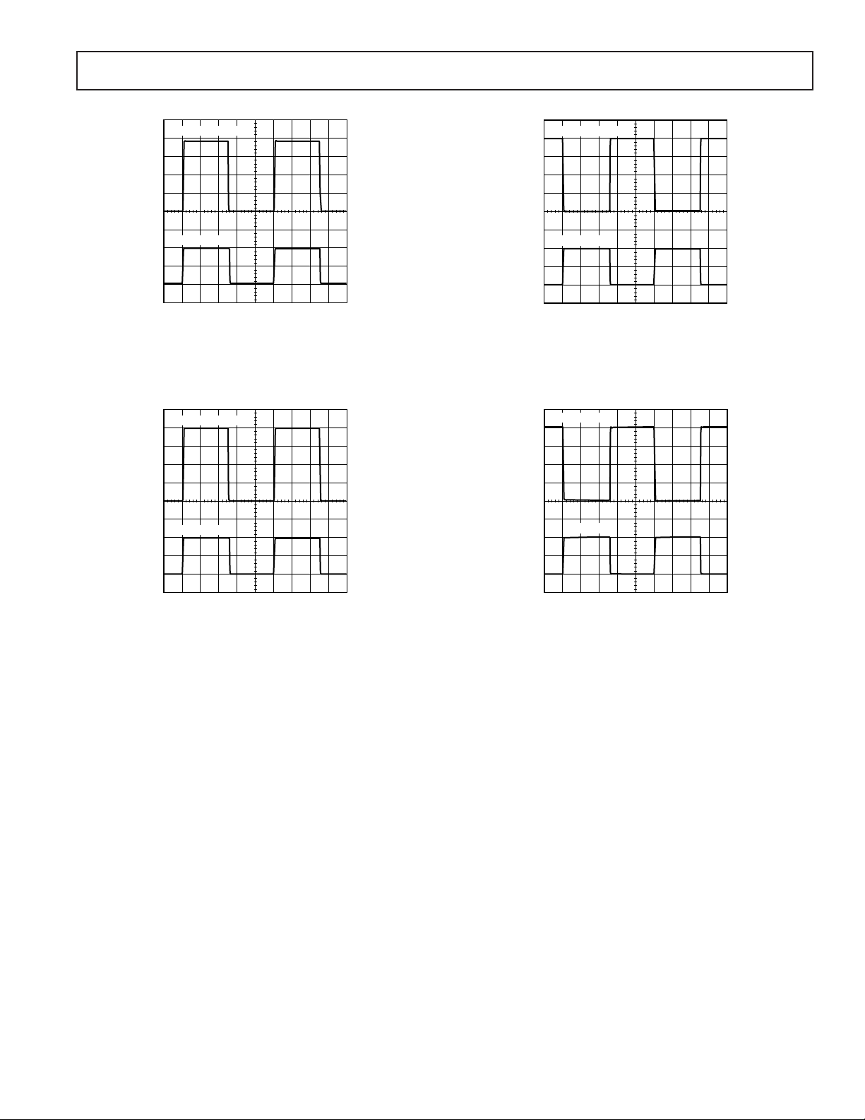
TPC 1. 100 mV Step Response; G = +2, VS = ±2.5 V
±
6 V, RL = 100
or
Ω
OUTPUT = 4V
1V/DIV
INPUT = 2V
OUTPUT = 100mV
INPUT = 100mV
50mV/DIV 25 mV/DIV
200ns/DIV
TPC 3. 100 mV Step Response; G = –1, VS = ±2.5 V
±
6 V, RL = 100
or
Ω
OUTPUT = 4V
INPUT = 4V
200ns/DIV
TPC 2. 4 V Step Response; G = +2, VS = ±6 V,
R
= 100
L
Ω
2V/DIV 1V/DIV
200ns/DIV
TPC 4. 4 V Step Response; G = –1, VS = ±6 V,
R
= 100
L
Ω
–5–REV. C
 Loading...