Low Power, High Output
Data Sheet
FEATURES
xDSL line driver that features full ADSL central office (CO)
Performance on ±12 V supplies
Low power operation
±5 V to ±12 V voltage supply
12.5 mA/amp (typical) total supply current
Power reduced keep alive current of 4.5 mA/amp
High output voltage and current drive
I
= 600 mA
OUT
40 V p-p differential output voltage R
Low single-tone distortion
–75 dBc @ 1 MHz SFDR, R
= 100 Ω, V
L
MTPR = –75 dBc, 26 kHz to 1.1 MHz, Z
P
= 20.4 dBm
LINE
High Speed
78 MHz bandwidth (–3 dB), G = +5
40 MHz gain flatness
1000 V/μs slew rate
= 50 Ω, VS = ±12 V
L
= 2 V p-p
OUT
= 100 Ω,
LINE
Current xDSL Line Driver
AD8016
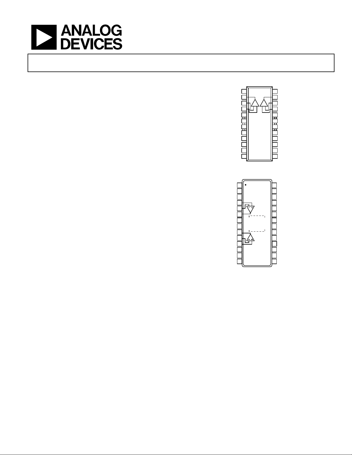
PIN CONFIGURATIONS
+V1 +V2
1
2
V
1
OUT
3
1
V
INN
4
V
1
INP
5
AGND
AGND
AGND
AGND
PWDN0
DGND
NC = NO CON NECT
AD8016
6
TOP VIEW
7
(Not to Scale)
8
9 16
10 15
11 14
–V1
12 13
NC
Figure 1. 24-Lead SOIC_W_BAT (RB-24)
1
NC NC
2
NC
3
NC
4
2
+V
IN
5
2
–V
IN
6
2
V
OUT
7
AD8016ARE
+V2
+V1
V
OUT
–V
IN
+V
IN
NC
NC
NC
NOTES
1. THE EXPOSED PADDLE IS FLOATING,
NOT ELECTRICALLY CONNECTED
INTERNALLY.
2. NC = NO CONNE CT.
8
9
1
10
1
11
1
12
13
14
TOP VIEW
(Not to Scale)
Figure 2. 28-Lead TSSOP_EP (RE-28-1)
+–
+–
24
23
22
21
20
19
18
17
28
27
26
25
24
23
22
21
20
19
18
17
16
15
V
OUT
2
V
INN
V
2
INP
AGND
AGND
AGND
AGND
PWDN1
BIAS
–V2
NC
NC
NC
NC
PWDN1
BIAS
–V2
–V1
DGND
NC
PWDN0
NC
NC
NC
2
01019-002
01019-003
GENERAL DESCRIPTION
The AD8016 high output current dual amplifier is designed for
the line drive interface in Digital Subscriber Line systems such
as ADSL, HDSL2, and proprietary xDSL systems. The drivers
are capable, in full-bias operation, of providing 24.4 dBm
output power into low resistance loads, enough to power a
20.4 dBm line, including hybrid insertion loss.
The AD8016 is available in a low cost 24-lead SOIC_W_BAT
and a 28-lead TSSOP_EP with an exposed lead frame (ePAD).
Operating from ±12 V supplies, the AD8016 requires only 1.5 W
of total power dissipation (refer to the Power Dissipation section
for details) while driving 20.4 dBm of power downstream using
Rev. C
Information furnished by Analog Devices is believed to be accurate and reliable. However, no
responsibility is assumed by Analog Devices for its use, nor for any infringements of patents or other
rights of third parties that may result from its use. Specifications subject to change without notice. No
license is granted by implication or otherwise under any patent or patent rights of Analog Devices.
Trademarks and registered trademarks are the property of their respective owners.
the xDSL hybrid in Figure 35 and Figure 36. Two digital bits
(PWDN0, PWDN1) allow the driver to be capable of full
performance, an output keep-alive state, or two intermediate
bias states. The keep-alive state biases the output transistors
enough to provide a low impedance at the amplifier outputs
for back termination.
The low power dissipation, high output current, high output
voltage swing, flexible power-down, and robust thermal
packaging enable the AD8016 to be used as the central office
(CO) terminal driver in ADSL, HDSL2, VDSL, and proprietary
xDSL systems.
One Technology Way, P.O. Box 9106, Norwood, MA 02062-9106, U.S.A.
Tel: 781.329.4700 www.analog.com
Fax: 781.461.3113 ©2012 Analog Devices, Inc. All rights reserved.

AD8016 Data Sheet
TABLE OF CONTENTS
Features .............................................................................................. 1
Pin Configurations ........................................................................... 1
General Description ......................................................................... 1
Revision History ............................................................................... 2
Specifications ..................................................................................... 3
Logic Inputs (CMOS Compatible Logic) .................................. 4
Absolute Maximum Ratings ............................................................ 5
Maximum Power Dissipation ..................................................... 5
ESD Caution .................................................................................. 5
Pin Configurations and Function Descriptions ........................... 6
Typical Performance Characteristics ............................................. 7
Test Circuts ...................................................................................... 13
Theory of Operation ...................................................................... 14
Power Supply and Decoupling .................................................. 14
Feedback Resistor Selection ...................................................... 14
Bias Pin and PWDN Features ................................................... 14
Thermal Shutdown .................................................................... 15
Applications Information .............................................................. 16
Multitone Power Ratio (MTPR) ............................................... 16
Generating DMT ........................................................................ 17
Power Dissipation....................................................................... 17
Thermal Enhancements and PCB Layout ............................... 18
Thermal Testing .......................................................................... 18
Air Flow Test Conditions .......................................................... 18
Experimental Results ................................................................. 19
Outline Dimensions ....................................................................... 20
Ordering Guide .......................................................................... 20
REVISION HISTORY
3/12—Rev. B to Rev. C
Updated Format .................................................................. Universal
Deleted PSOP Package and Evaluation Boards (Throughout) ... 1
Added Pin Configurations and Function Descriptions Sections .. 7
Updated Outline Dimensions ....................................................... 21
Changes to Ordering Guide .......................................................... 19
11/03—Rev. A to Rev. B
Changes to Ordering Guide ............................................................ 4
Changes to TPC 21 ........................................................................... 8
Updated Outline Dimensions ..................................................19-20
Rev. C | Page 2 of 20

Data Sheet AD8016
Bandwidth for 0.1 dB Flatness
G = +5, RF = 499 Ω, V
= 0.2 V p-p
16
38 MHz
Peaking
V
= 0.2 V p-p < 50 MHz
0.1 dB
Multitone Power Ratio1
26 kHz to 1.1 MHz, Z
= 100 Ω, P
= 20.4 dBm
–75 dBc
IMD
500 kHz, Δf = 10 kHz, RL = 100 Ω/25 Ω
−84/−80
−88/−85
dBc
Input Capacitance
2 pF
Input Common-Mode Voltage Range
−10 +10
V
SPECIFICATIONS
@ 25°C, VS = ±12 V, RL = 100 Ω, PWDN0, PWDN1 = (1, 1), T
Table 1.
Parameter Test Conditions/Comments Min Typ Max Unit
DYNAMIC PERFORMANCE
−3 dB Bandwidth G = +1, RF = 1.5 kΩ, V
G = +5, RF = 499 Ω, V
Large Signal Bandwidth V
Slew Rate V
Rise and Fall Time V
Settling Time 0.1%, V
Input Overdrive Recovery Time V
NOISE/DISTORTION PERFORMANCE
Distortion, Single-Ended V
Second Harmonic fC = 1 MHz, RL = 100 Ω/25 Ω −75/−62 −77/−64 dBc
Third Harmonic fC = 1 MHz, RL = 100 Ω/25 Ω −88/−74 −93/−76 dBc
IP3 500 kHz, RL = 100 Ω/25 Ω 42/40 43/41 dBm
Voltage Noise (RTI) f = 10 kHz 2.6 4.5 nV/√Hz
Input Current Noise f = 10 kHz 18 21 pA√Hz
INPUT CHARACTERISTICS
RTI Offset Voltage −3.0 1.0 +3.0 mV
+Input Bias Current −45 +45 μA
–Input Bias Current −75 4 +75 μA
Input Resistance 400 kΩ
= 4 V p-p 90 MHz
OUT
OUT
= 4 V p-p, G = +2 1000 V/μs
OUT
= 2 V p-p 2 ns
OUT
= 2 V p-p 23 ns
OUT
= 12.5 V p-p 350 ns
OUT
= 2 V p-p, G = +5, RF = 499 Ω
OUT
= −40°C, T
MIN
= 0.2 V p-p 380 MHz
OUT
< 0.5 V p-p 69 78 MHz
OUT
OUT
LINE
= +85°C, unless otherwise noted.
MAX
LINE
Common-Mode Rejection Ratio 58 64 dB
OUTPUT CHARACTERISTICS
Output Voltage Swing Single-ended, RL = 100 Ω −11 +11 V
Linear Output Current G = 5, RL = 10 Ω, f1 = 100 kHz, −60 dBc SFDR 400 600 mA
Short-Circuit Current 2000 mA
Capacitive Load Drive 80 pF
POWER SUPPLY
Operating Range ±3 ±13 V
Quiescent Current PWDN1, PWDN0 = (1, 1) 12.5 13.2 mA/Amp
PWDN1, PWDN0 = (1, 0) 8 10 mA/Amp
PWDN1, PWDN0 = (0, 1) 5 8 mA/Amp
PWDN1, PWDN0 = (0, 0) 4 6 mA/Amp
Recovery Time To 95% of IQ 25 μs
Shutdown Current 250 μA out of bias pin 1.5 4.0 mA/Amp
Power Supply Rejection Ratio ΔVS = ±1 V 63 75 dB
OPERATING TEMPERATURE RANGE −40 +85 °C
1
See Figure 48, R20, R21 = 0 Ω, R1 = open.
Rev. C | Page 3 of 20

AD8016 Data Sheet
PWDN1, PWDN0 = (1, 0)
6
6.9
mA/Amp
PWDN1, PWDN0 = (0, 1)
4
5.0
mA/Amp
@ 25°C, VS = ±6 V, RL = 100 Ω, PWDN0, PWDN1 = (1, 1), T
Table 2.
Parameter Test Conditions/Comments Min Typ Max Unit
DYNAMIC PERFORMANCE
–3 dB Bandwidth G = +1, RF = 1.5 kΩ, V
G = +5, RF = 499 Ω, V
Bandwidth for 0.1 dB Flatness G = +5, RF = 499 Ω, V
Large Signal Bandwidth V
Peaking V
Slew Rate V
Rise and Fall Time V
Settling Time 0.1%, V
Input Overdrive Recovery Time V
NOISE/DISTORTION PERFORMANCE
Distortion, Single-Ended G = +5, V
Second Harmonic fC = 1 MHz, RL = 100 Ω/25 Ω −73/61 −75/−63 dBc
Third Harmonic fC = 1 MHz, RL = 100 Ω/25 Ω −80/−68 −82/−70 dBc
Multitone Power Ratio1 26 kHz to 138 kHz, Z
IMD 500 kHz, Δf = 110 kHz, RL = 100 Ω/25 Ω −87/−82 −88/−83 dBc
IP3 500 kHz 42/39 42/39 dBm
Voltage Noise (RTI) f = 10 kHz 4 5 nV/√Hz
Input Current Noise f = 10 kHz 17 20 pA√Hz
INPUT CHARACTERISTICS
RTI Offset Voltage −3.0 0.2 +3.0 mV
+Input Bias Current −25 10 +25 μA
−Input Bias Current −30 10 +30 μA
Input Resistance 400 kΩ
Input Capacitance 2 pF
Input Common-Mode Voltage Range −4 +4 V
Common-Mode Rejection Ratio 60 66 dB
OUTPUT CHARACTERISTICS
Output Voltage Swing Single-Ended, RL = 100 Ω −5 +5 V
Linear Output Current G = +5, RL = 5 Ω, f = 100 kHz, −60 dBc SFDR 300 420 mA
Short-Circuit Current 830 mA
Capacitive Load Drive RS = 10 Ω 50 pF
POWER SUPPLY
Quiescent Current PWDN1, PWDN0 = (1, 1) 8 9.7 mA/Amp
= 1 V rms 80 MHz
OUT
= 0.2 V p-p < 50 MHz 0.7 1.0 dB
OUT
= 4 V p-p, G = +2 300 V/μs
OUT
= 2 V p-p 2 ns
OUT
= 2 V p-p 39 ns
OUT
= 6.5 V p-p 350 ns
OUT
= 2 V p-p, RF = 499 Ω
OUT
= –40°C, T
MIN
= 0.2 V p-p 320 MHz
OUT
< 0.5 V p-p 70 71 MHz
OUT
= 0.2 V p-p 10 15 MHz
OUT
= 100 Ω, P
LINE
= +85°C, unless otherwise noted.
MAX
= 13 dBm −68 dBc
LINE
PWDN1, PWDN0 = (0, 0) 3 4.1 mA/Amp
Recovery Time To 95% of IQ 23 μs
Shutdown Current 250 μA out of bias pin 1.0 2.0 mA/Amp
Power Supply Rejection Ratio ΔVS = ±1 V 63 80 dB
OPERATING TEMPERATURE RANGE −40 +85 °C
1
See Figure 48, R20, R21 = 0 Ω, R1 = open.
LOGIC INPUTS (CMOS COMPATIBLE LOGIC)
PWDN0, PWDN1, VCC = ±12 V or ±6 V; full temperature range.
Table 3.
Parameter Min Typ Max Unit
Logic 1 Voltage 2.2 VCC V
Logic 0 Voltage 0 0.8 V
Rev. C | Page 4 of 20

Data Sheet AD8016
A
ABSOLUTE MAXIMUM RATINGS
Table 4.
Parameter Rating
Supply Voltage 26.4 V
Internal Power Dissipation
SOIC_W_BAT Package1 1.4 W
TSSOP_EP Package2 1.4 W
Input Voltage (Common-Mode) ±VS
Differential Input Voltage ±VS
Output Short-Circuit Duration Observe power derating
Storage Temperature Range −65°C to +125°C
Operating Temperature Range −40°C to +85°C
Lead Temperature Range (Soldering 10 sec) 300°C
1
Specification is for device on a 4-layer board with 10 inches2 of 1 oz copper
at 85°C 24-lead SOIC_W_BAT package: θ
2 Specification is for device on a 4-layer board with 9 inches2 of 1 oz copper at
85°C 28-lead (TSSOP_EP) package: θJA = 29°C/W.
= 28°C/W.
JA
curves
Stresses above those listed under Absolute Maximum Ratings
may cause permanent damage to the device. This is a stress
rating only; functional operation of the device at these or any
other conditions above those indicated in the operational
section of this specification is not implied. Exposure to absolute
maximum rating conditions for extended periods may affect
device reliability.
MAXIMUM POWER DISSIPATION
The maximum power that can be safely dissipated by the
AD8016 is limited by the associated rise in junction temper-
ature. The maximum safe junction temperature for a plastic
encapsulated device is determined by the glass transition
temperature of the plastic, approximately 150°C. Temporarily
exceeding this limit may cause a shift in parametric performance due to a change in the stresses exerted on the die by
the package.
The output stage of the AD8016 is designed for maximum load
current capability. As a result, shorting the output to common
can cause the AD8016 to source or sink 2000 mA. To ensure
proper operation, it is necessary to observe the maximum
power derating curves. Direct connection of the output to
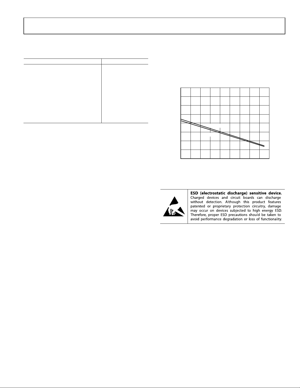
either power supply rail can destroy the device.
8
7
6
TION (W)
5
4
3
2
MAXIMUM POWER DISSIP
1
0
010
Figure 3. Maximum Power Dissipation vs. Temperature for AD8016 for
SOIC_W_BAT
TSSOP-EP
20 30 40 50 60 70 80 90
AMBIENT TEMPERATURE (°C)
T
= 125 °C
J
01019-005
ESD CAUTION
Rev. C | Page 5 of 20

AD8016 Data Sheet
PIN CONFIGURATIONS AND FUNCTION DESCRIPTIONS
+V1 +V2
1
2
V
1
OUT
3
1
V
INN
4
V
1
INP
5
AGND
6
AGND
7
AGND
8
AGND
9 16
PWDN0
10 15
DGND
11 14
–V1
12 13
NC
NC = NO CON NECT
+–
+–
AD8016
TOP VIEW
(Not to Scale)
24
23
22
21
20
19
18
17
V
OUT
2
V
INN
V
2
INP
AGND
AGND
AGND
AGND
PWDN1
BIAS
–V2
NC
1
NC NC
2
NC
3
NC
4
+V
2
IN
5
–V
2
IN
6
V
2
2
01019-002
OUT
7
AD8016ARE
+V2
+V1
V
OUT
–V
IN
+V
IN
NC
NC
NC
NOTES
1. THE EXPOSED PADDLE IS FLOATING,
NOT ELECTRICALLY CONNECTED
INTERNALLY.
2. NC = NO CONNE CT.
8
9
1
10
1
11
1
12
13
14
TOP VIEW
(Not to Scale)
28
27
26
25
24
23
22
21
20
19
18
17
16
15
NC
NC
NC
PWDN1
BIAS
–V2
–V1
DGND
NC
PWDN0
NC
NC
NC
01019-003
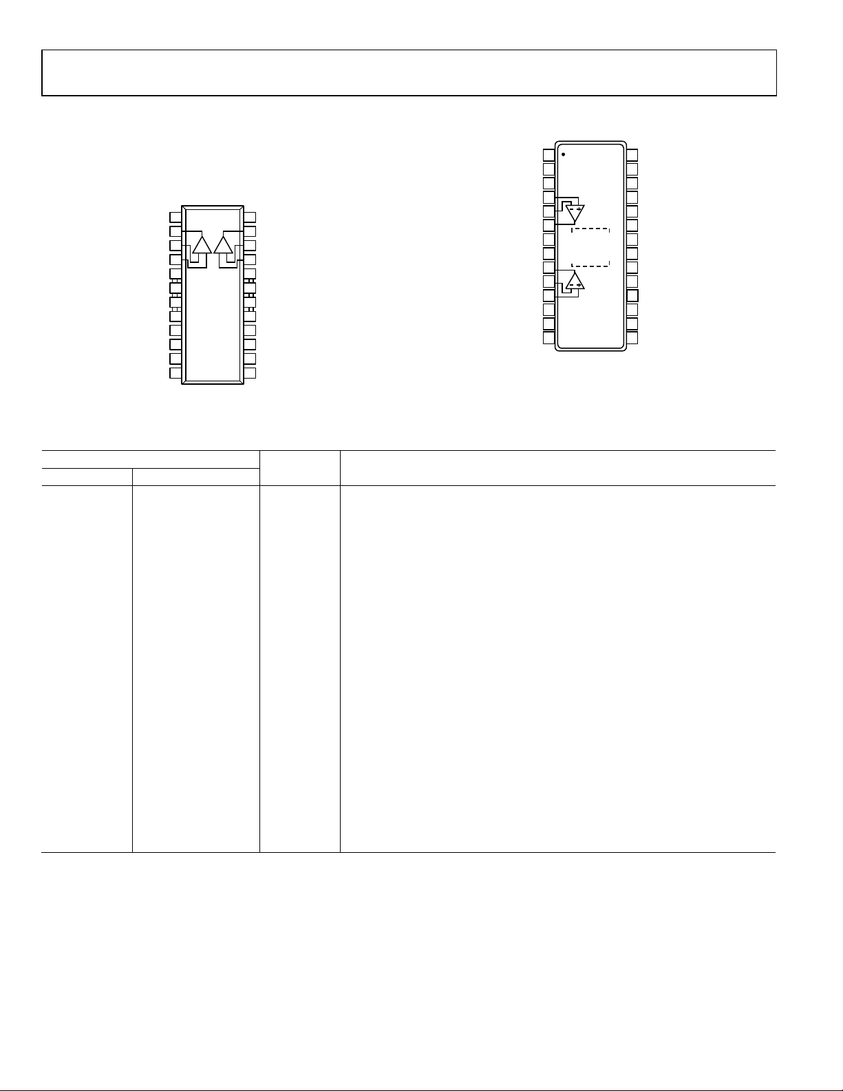
Figure 4. 24-Lead SOIC_W_BAT (RB-24) Figure 5. 28-Lead TSSOP_EP (RE-28-1)
Table 5. Pin Function Descriptions
Pin No.
Mnemonic Description SOIC_W_BAT TSSOP_EP
1 8 +V1 Positive Power Supply, Amp 1.
2 9 V
3 V
4 V
1 Output Signal, Amp 1.
OUT
1 Negative Input Signal, Amp 1.
INN
1 Positive Input Signal, Amp1.
INP
5 to 8, 17 to 20 AGND Analog Ground.
9 18 PWDN0 Power-Down Input 0.
10 20 DGND Digital Ground.
11 21 −V1 Negative Power Supply, Amp1.
12, 13
1 to 3, 12 to 17, 19,
NC This pin is not connected internally (see Figure 4 and Figure 5).
25 to 28
14 22 −V2 −V Power Supply, Amp 2.
15 23 BIAS Quiescent Current Adjust.
16 24 PWDN1 Power-Down Input 1.
21 V
22 V
23 6 V
2 Positive Input Signal, Amp 2.
INP
2 Negative Input Signal, Amp 2.
INN
2 Output Signal, Amp 2.
OUT
24 7 +V2 Positive Power Supply, Amp 2.
4 +VIN2 Positive Input Signal, Amp 2.
5 −VIN2 Negative Input Signal, Amp 2.
10 −VIN1 Negative Input Signal, Amp 1.
11 +VIN1 Positive Input Signal, Amp 1.
EP EPAD Exposed Pad. The exposed paddle is floating, not electrically connected internally.
Rev. C | Page 6 of 20
 Loading...