Wideband/Differential Output
a
FEATURES
Low Cost, Wide Bandwidth, Low Noise
Bandwidth: 240 MHz
Pulse Width Modulation: 500 ps
Rise Time/Fall Time: 1.5 ns
Input Current Noise: 3.0 pA/√
Total Input RMS Noise: 26.5 nA to 100 MHz
Wide Dynamic Range
Optical Sensitivity: –36 dBm @ 155.52 Mbps
Peak Input Current: 6350 mA
Differential Outputs
Low Power: 5 V @ 25 mA
Wide Operating Temperature Range: –408C to +858C
APPLICATIONS
Fiber Optic Receivers: SONET/SDH, FDDI, Fibre Channel
Stable Operation with High Capacitance Detectors
Low Noise Preamplifiers
Single-Ended to Differential Conversion
I-to-V Converters
Hz @ 100 MHz
Transimpedance Amplifier
AD8015
FUNCTIONAL BLOCK DIAGRAM
25.0E+3
20.0E+3
15.0E+3
1
NC
I
2
IN
3
NC
V
4
BYP
NC = NO CONNECT
AD8015
10kΩ
G = 30
+1
G = 3
+1
– + +V
1.7V
DIFFERENTIAL
50Ω
S
50Ω
+V
8
+OUTPUT
7
–OUTPUT
6
5
–V
S
S
PRODUCT DESCRIPTION
The AD8015 is a wide bandwidth, single supply transimpedance
amplifier optimized for use in a fiber optic receiver circuit. It is a
complete, single chip solution for converting photodiode current
into a differential voltage output. The 240MHz bandwidth enables
AD8015 application in FDDI receivers and SONET/SDH
receivers with data rates up to 155 Mbps. This high bandwidth
supports data rates beyond 300 Mbps. The differential outputs
drive ECL directly, or can drive a comparator/ fiber optic post
amplifier.
In addition to fiber optic applications, this low cost, silicon alternative to GaAs-based transimpedance amplifiers is ideal for
systems requiring a wide dynamic range preamplifier or singleended to differential conversion. The IC can be used with a
standard ECL power supply (–5.2 V) or a PECL (+5 V) power
supply; the common mode at the output is ECL compatible.
The AD8015 is available in die form, or in an 8-pin SOIC
package.
10.0E+3
X-RESISTANCE – Ω
5.0E+3
000.E+0
10.0E+6 100.0E+6 1.0E+9
SINGLE-ENDED
FREQUENCY – Hz
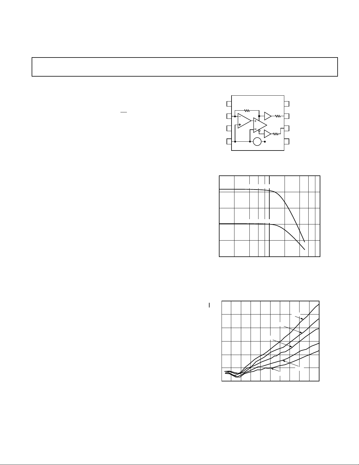
Figure 1. Differential/Single-Ended Transimpedance vs.
Frequency
5.0
Hz
√
4.5
4.0
3.5
3.0
2.5
EQUIVALENT INPUT CURRENT NOISE – pA
2.0
1.5pF
FREQUENCY – Hz
3.0pF
2.0pF
1.0pF
0.5pF
100.0E+620.0E+6000.0E+0 80.0E+660.0E+640.0E+6
REV. A
Information furnished by Analog Devices is believed to be accurate and
reliable. However, no responsibility is assumed by Analog Devices for its
use, nor for any infringements of patents or other rights of third parties
which may result from its use. No license is granted by implication or
otherwise under any patent or patent rights of Analog Devices.
Figure 2. Noise vs. Frequency (SO-8 Package with
Added Capacitance)
© Analog Devices, Inc., 1996
One Technology Way, P.O. Box 9106, Norwood, 02062-9106, U.S.A.
Tel: 617/329-4700 Fax: 617/326-8703

AD8015–SPECIFICA TIONS
WARNING!
ESD SENSITIVE DEVICE
(SO Package @ TA = +258C and VS = +5 V, unless otherwise noted)
AD8015AR
Parameter Conditions Min Typ Max Units
DYNAMIC PERFORMANCE
Bandwidth 3 dB 180 240 MHz
Pulse Width Modulation 10 µA to 200 µA Peak 500 ps
Rise and Fall Time 10% to 90% 1.5 ns
Settling Time
1
to 3%, 0.5 V Diff Output Step 3 ns
INPUT
Linear Input Current Range ±2.5%, Nonlinearity ±25 ±30 µA
Max Input Current Range Saturation ±200 ±350 µA
Optical Sensitivity 155 Mbps, Avg Power –36 dBm
Input Stray Capacitance Die, by Design 0.2 pF
SOIC, by Design 0.4 pF
Input Bias Voltage +VS to I
NOISE Die, Single Ended at P
or Differential (P
C
STRAY
and V
IN
= 0.3 pF
BYP
OUT
OUT–NOUT
1.6 1.8 2.0 V
,
),
Input Current Noise f = 100 MHz 3.0 pA/√
Total Input RMS Noise DC to 100 MHz 26.5 nA
TRANSFER CHARACTERISTICS
Transresistance Single Ended 8 10 12 kΩ
Differential 16 20 24 kΩ
Power Supply Single Ended 37.0 dB
Rejection Ratio Differential 40 dB
Hz
OUTPUT
Differential Offset 620mV
Output Common-Mode Voltage From Positive Supply –1.5 –1.3 –1.1 V
Voltage Swing (Differential) Positive Input Current, R
Positive Input Current, R
= ∞ 1.0 V p-p
L
= 50 Ω 600 mV p-p
L
Output Impedance 40 50 60 Ω
POWER SUPPLY T
MIN
to T
MAX
Operating Range Single Supply +4.5 +5 +11 V
Dual Supply ±2.25 ±5.5 V
Current 25 26 mA
NOTES
1
Settling Time is defined as the time elapsed from the application of a perfect step input to the time when the output has entered and remained within a specified error
band symmetrical about the final value. This parameter includes propagation delay, slew time, overload recovery, and linear settling times.
Specifications subject to change without notice.
ABSOLUTE MAXIMUM RATINGS
Supply Voltage (+VS to –VS). . . . . . . . . . . . . . . . . . . . . . . 12 V
Internal Power Dissipation
2
1
Small Outline . . . . . . . . . . . . . . . . . . . . . . . . . . . . 0.9 Watts
Output Short Circuit Duration . . . . . . . . . . . . . . . Indefinite
Maximum Input Current . . . . . . . . . . . . . . . . . . . . . . . . 10 mA
Storage Temperature Range . . . . . . . . . . . . –65°C to +125°C
Operating Temperature Range (T
MIN
to T
MAX
)
AD8015ACHIP/AR . . . . . . . . . . . . . . . . . . –40°C to +85°C
Maximum Junction Temperature . . . . . . . . . . . . . . . . . +165°C
Lead Temperature Range (Soldering 10 sec) . . . . . . . . +300°C
NOTES
1
Stresses above those listed under “Absolute Maximum Ratings” may cause
permanent damage to the device. This is a stress rating only and functional
operation of the device at these or any other conditions above those indicated in the
operational section of this specification is not implied. Exposure to absolute
maximum rating conditions for extended periods may affect device reliability.
2
Specification is for device in free air: 8-pin SOIC package: θJA = 155°C/W.
ORDERING GUIDE
Temperature Package Package
Model Range Description Option
AD8015AR –40°C to +85°C 8-Pin Plastic SOIC SO-8
AD8015ACHIPS –40°C to +85°C Die Fo
rm
CAUTION
ESD (electrostatic discharge) sensitive device. Electrostatic charges as high as 4000 V readily
accumulate on the human body and test equipment and can discharge without detection.
Although the AD8015 features proprietary ESD protection circuitry, permanent damage may
occur on devices subjected to high energy electrostatic discharges. Therefore, proper ESD
precautions are recommended to avoid performance degradation or loss of functionality.
–2–
REV. A

V1
+V
S
CLOCK
RECOVERY
LPF:
3dB@
0.7 x F
LPF:
3dB@
0.7 x F
QUANTIZER
R > 40Ω
C1 >100pF
4.5V < V
S
< 11V
CLK
DATA
RR
C1
10kΩ
5
6
7
8
4
3
2
1
AD8015
50Ω
+1
G = 3
G = 30
50Ω
+1
– + +V
S
1.7V
1.7V
+V
S
PIN CONFIGURATION
AD8015
AD8015
1
NC
I
IN
NC
V
BYP
10kΩ
2
G = 30
3
4
NC = NO CONNECT
G = 3
– + +V
1.7V
+1
50Ω
+1
S
METALIZATION PHOTOGRAPH
Dimensions shown in microns. Not to scale.
OPTIONAL
+V
CONNECTION
S
+V
50Ω
S
+V
8
+OUTPUT
7
–OUTPUT
6
5
–V
S
.
S
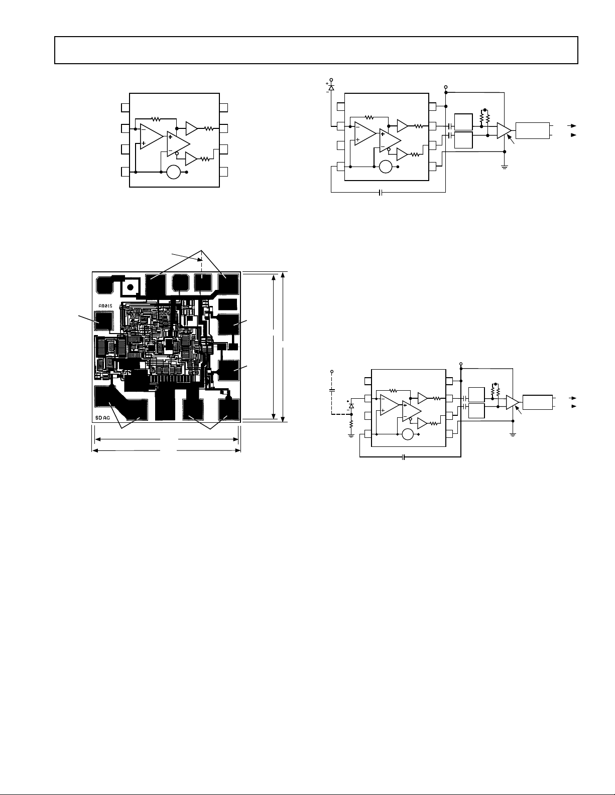
Figure 3. Fiber Optic Receiver Application: Photodiode
Referred to Positive Supply
PHOTODIODE REFERRED TO NEGATIVE SUPPLY
Figure 4 shows the AD8015 used in a circuit where the photodiode is referred to the negative supply. This results in a larger
back bias voltage than when referring the photodiode to the
positive supply. The larger back bias voltage on the photodiode
I
IN
V
BYP
NOTE:
FOR BEST PERFORMANCE ATTACH PACKAGE
SUBSTRATE TO +VS.
MATERIAL AT BACK OF DIE IS SILICON. USE OF
OR –VS FOR DIE ATTACH IS ACCEPTABLE.
+V
S
813µ
973µ
–V
S
+OUTPUT
838µ
998µ
–OUTPUT
decreases the photodiode’s capacitance thereby increasing its
bandwidth. The R2, C2 network shown in Figure 4 is added to
decouple the photodiode to the positive supply. This improves
PSRR.
+V
+V
S
C2
+V
S
1.7V
R2
1
2
3
4
AD8015
10kΩ
G = 30
G = 3
– + +V
1.7V
C1
50Ω
+1
50Ω
+1
S
S
LPF:
3dB@
0.7 x F
LPF:
3dB@
0.7 x F
V1
RR
RECOVERY
QUANTIZER
R > 40Ω
C1 >100pF
4.5V < V
R2 AND C2 OPTIONAL
FOR IMPROVED PSRR
< 11V
S
DATA
CLK
CLOCK
8
7
6
5
Figure 4. Fiber Optic Receiver Application: Photodiode
Referred to Negative Supply
FIBER OPTIC RECEIVER APPLICATIONS
In a fiber optic receiver, the photodiode can be placed from the
I
pin to either the positive or negative supply. The AD8015
IN
converts the current from the photodiode to a differential voltage in these applications. The voltage at the V
pin is ≈1.8 V
BYP
below the positive supply. This node must be bypassed with a
capacitor (C1 in Figures 3 and 4 below) to the signal ground. If
large levels of power supply noise exist, then connecting C1 to
+V
is recommended for improved noise immunity. For opti-
S
mum performance, choose C1 such that C1 > 1/(2 π × 1000 ×
f
); where f
MIN
is the minimum useful
MIN
frequency in Hz.
FIBER OPTIC SYSTEM NOISE PERFORMANCE
The AD8015 maintains 26.5 nA referred to input (RTI) to 100
MHz. Calculations below translate this specification into minimum power level and bit error rate specifications for SONET
and FDDI systems. The dominant sources of noise are: 10 kΩ
feedback resistor current noise, input bipolar transistor base
current noise, and input voltage noise.
The AD8015 has dielectrically isolated devices and bond pads
that minimize stray capacitance at the I
pin. Input voltage
IN
noise is negligible at lower frequencies, but can become the
dominant noise source at high frequencies due to I
capacitance. Minimizing the stray capacitance at the I
pin stray
IN
pin is
IN
critical to maintaining low noise levels at high frequencies. The
PHOTODIODE REFERRED TO POSITIVE SUPPLY
Figure 3 shows the AD8015 used in a circuit where the photodiode is referred to the positive supply. The back bias voltage on
the photodiode is ≈1.8 V. This method of referring the photodiode provides greater power supply noise immunity (PSRR)
than referring the photodiode to the negative supply. The signal
path is referred to the positive rail, and the photodiode capacitance is not modulated by high frequency noise that may exist
on the negative rail.
REV. A
pins surrounding the I
connection and should be left unconnected in an application.
This minimizes I
ground plane or metal runs near Pins 1, 2, and 3 and to minimize capacitance at the I
The AD8015AR (8-pin SOIC) I
0.4 pF without the photodiode. Photodiodes used for SONET
or FDDI systems typically add 0.3 pF, resulting in roughly
0.7 pF total stray capacitance.
–3–
pin (Pins 1 and 3) have no internal
IN
pin package capacitance. It is best to have no
IN
pin.
IN
pin total stray capacitance is
IN
 Loading...