

Analog Devices AD8011 c Datasheet
300 MHz
DISTORTION (dBc)
–40
–100
–60
–80
FREQUENCY (MHz)
10 20
THIRD
R
L
= 150⍀
SECOND
R
L
= 150⍀
THIRD
R
L
=1k⍀
SECOND
R
L
= 1k⍀
G = +2
Current Feedback Amplifier
FEATURES
Easy to Use
Low Power
1 mA Power Supply Current (5 mW on 5 V
High Speed and Fast Settling on 5 V
300 MHz, –3 dB Bandwidth (G = +1)
180 MHz, –3 dB Bandwidth (G = +2)
2000 V/s Slew Rate
29 ns Settling Time to 0.1%
Good Video Specifications (R
= 1 k⍀, G = +2)
L
Gain Flatness 0.1 dB to 25 MHz
0.02% Differential Gain Error
0.06ⴗ Differential Phase Error
Low Distortion
–70 dBc Worst Harmonic @ 5 MHz
–62 dBc Worst Harmonic @ 20 MHz
Single Supply Operation
Fully Specified for 5 V Supply
APPLICATIONS
Power Sensitive, High Speed Systems
Video Switchers
Distribution Amplifiers
A-to-D Driver
Professional Cameras
CCD Imaging Systems
Ultrasound Equipment (Multichannel)
5
G = +2
4
R
= 1k⍀
F
= +5V OR ⴞ5V
V
S
3
= 200mV p-p
V
OUT
2
1
0
–1
–2
NORMALIZED GAIN (dB)
–3
–4
–5
1
10
FREQUENCY (MHz)
100 500
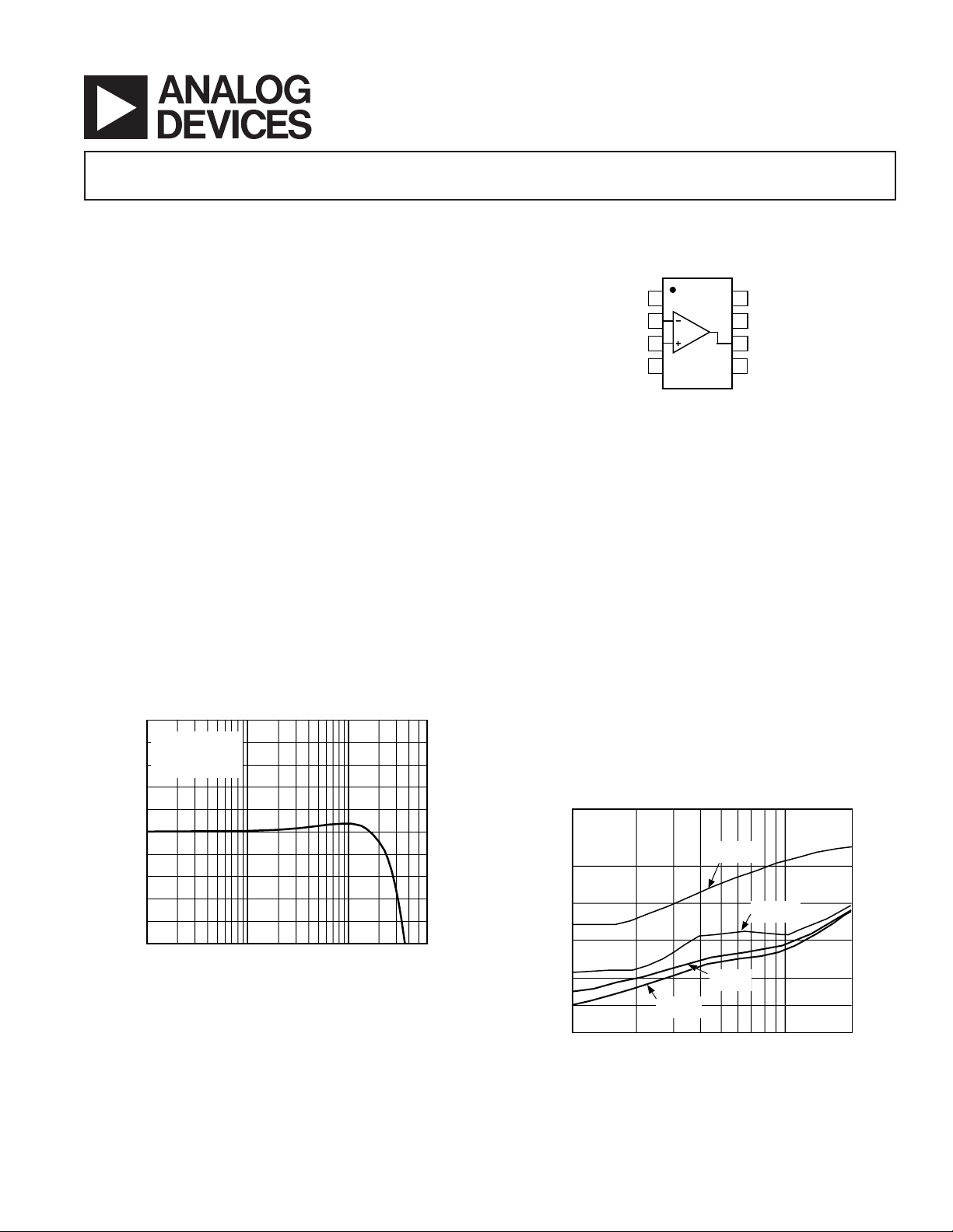
Figure 1. Frequency Response; G = +2, VS = +5 V, or ±5 V
*Protected under Patent Number 5,537,079.
AD8011
*
FUNCTIONAL BLOCK DIAGRAM
8-Lead PDIP and SOIC
)
S
NC
1
2
–IN
3
+IN
4
V–
AD8011
NC = NO CONNECT
8
NC
V+
7
OUT
6
NC
5
PRODUCT DESCRIPTION
The AD8011 is a very low power, high speed amplifier designed
to operate on +5 V or ± 5 V supplies. With wide bandwidth,
low distortion, and low power, this device is ideal as a generalpurpose amplifier. It also can be used to replace high speed
amplifiers consuming more power. The AD8011 is a current feedback amplifier and features gain flatness of 0.1 dB to 25 MHz
while offering differential gain and phase error of 0.02% and 0.06°
on a single 5 V supply. This makes the AD8011 ideal for professional video electronics such as cameras, video switchers, or any
high speed portable equipment. Additionally, the AD8011’s low
distortion and fast settling make it ideal for buffering high speed
8-, 10-, and 12-bit A-to-D converters.
The AD8011 offers very low power of 1 mA maximum and can
run on single 5 V to 12 V supplies. All this is offered in a small
8-lead PDIP or 8-lead SOIC package. These features fit well with
portable and battery-powered applications where size and power
are critical.
The AD8011 is available in the industrial temperature range of
–40°C to +85°C.
REV. C
Information furnished by Analog Devices is believed to be accurate and
reliable. However, no responsibility is assumed by Analog Devices for its
use, nor for any infringements of patents or other rights of third parties that
may result from its use. No license is granted by implication or otherwise
under any patent or patent rights of Analog Devices. Trademarks and
registered trademarks are the property of their respective companies.
Figure 2. Distortion vs. Frequency; VS = ±5 V
One Technology Way, P.O. Box 9106, Norwood, MA 02062-9106, U.S.A.
Tel: 781/329-4700 www.analog.com
Fax: 781/326-8703 © 2003 Analog Devices, Inc. All rights reserved.

AD8011–SPECIFICATIONS
DUAL SUPPLY
(@ TA = 25ⴗC, VS = ⴞ5 V, G = +2, RF = 1 k⍀, RL = 1 k⍀, unless otherwise noted.)
AD8011A
Parameter Conditions Min Typ Max Unit
DYNAMIC PERFORMANCE
–3 dB Small Signal Bandwidth, VO < 1 V p-p G = +1 340 400 MHz
–3 dB Small Signal Bandwidth, V
–3 dB Large Signal Bandwidth, V
< 1 V p-p G = +2 180 210 MHz
O
= 5 V p-p G = +10, RF = 500 Ω 57 MHz
O
Bandwidth for 0.1 dB Flatness G = +2 20 25 MHz
Slew Rate G = +2, V
G = –1, V
Settling Time to 0.1% G = +2, V
Rise and Fall Time G = +2, V
= 4 V Step 3500 V/µs
O
= 4 V Step 1100 V/µs
O
= 2 V Step 25 ns
O
= 2 V Step 0.4 ns
O
G = –1, VO = 2 V Step 3.7 ns
NOISE/HARMONIC PERFORMANCE
Second Harmonic f
Third Harmonic R
= 5 MHz, VO = 2 V p-p, G = +2
C
= 1 kΩ –75 dB
R
L
R
= 150 Ω –67 dB
L
= 1 kΩ –70 dB
L
= 150 Ω –54 dB
R
L
Input Voltage Noise f = 10 kHz 2 nV/√Hz
Input Current Noise f = 10 kHz, +In 5 pA/√Hz
–In 5 pA/√Hz
Differential Gain Error NTSC, G = +2, R
R
Differential Phase Error NTSC, G = +2, R
= 1 kΩ 0.02 %
L
= 150 Ω 0.02 %
L
= 1 kΩ 0.06 Degrees
L
RL = 150 Ω 0.3 Degrees
DC PERFORMANCE
Input Offset Voltage 25±mV
T
MIN–TMAX
26±mV
Offset Drift 10 µV/°C
–Input Bias Current 515±µA
T
MIN–TMAX
20 ±µA
+Input Bias Current 515±µA
T
MIN–TMAX
20 ±µA
Open-Loop Transresistance 800 1300 kΩ
T
MIN–TMAX
550 kΩ
INPUT CHARACTERISTICS
Input Resistance +Input 450 kΩ
Input Capacitance +Input 2.3 pF
Input Common-Mode Voltage Range 3.8 4.1 ±V
Common-Mode Rejection Ratio
Offset Voltage VCM = ±2.5 V –52 –57 dB
OUTPUT CHARACTERISTICS
Output Voltage Swing 3.9 4.1 ±V
Output Resistance 0.1 0.3 Ω
Output Current T
MIN–TMAX
15 30 mA
Short-Circuit Current 60 mA
POWER SUPPLY
Operating Range ±1.5 ±6.0 V
Quiescent Current T
MIN–TMAX
1.0 1.3 mA
Power Supply Rejection Ratio VS = ±5 V ± 1 V 55 58 dB
Specifications subject to change without notice.
REV. C–2–

AD8011
SINGLE SUPPLY
(@ TA = 25ⴗC, VS = 5 V, G = +2, RF = 1 k⍀, VCM = 2.5 V, RL = 1 k⍀, unless otherwise noted.)
AD8011A
Parameter Conditions Min Typ Max Unit
DYNAMIC PERFORMANCE
–3 dB Small Signal Bandwidth, V
–3 dB Small Signal Bandwidth, V
–3 dB Large Signal Bandwidth, V
< 0.5 V p-p G = +1 270 328 MHz
O
< 0.5 V p-p G = +2 150 180 MHz
O
= 2.5 V p-p G = +10, RF = 500 Ω 57 MHz
O
Bandwidth for 0.1 dB Flatness G = +2 15 20 MHz
Slew Rate G = +2, V
G = –1, V
Settling Time to 0.1% G = +2, V
Rise and Fall Time G = +2, V
= 2 V Step 2000 V/µs
O
= 2 V Step 500 V/µs
O
= 2 V Step 29 ns
O
= 2 V Step 0.6 ns
O
G = –1, VO = 2 V Step 4 ns
NOISE/HARMONIC PERFORMANCE
Second Harmonic f
= 5 MHz, VO = 2 V p-p, G = +2
C
RL = 1 kΩ –84 dB
= 150 Ω –67 dB
R
Third Harmonic R
L
= 1 kΩ –76 dB
L
= 150 Ω –54 dB
R
L
Input Voltage Noise f = 10 kHz 2 nV/√Hz
Input Current Noise f = 10 kHz, +In 5 pA/√Hz
–In 5 pA/√Hz
Differential Gain Error NTSC, G = +2, R
R
Differential Phase Error NTSC, G = +2, R
= 1 kΩ 0.02 %
L
= 150 Ω 0.6 %
L
= 1 kΩ 0.06 Degrees
L
RL = 150 Ω 0.8 Degrees
DC PERFORMANCE
Input Offset Voltage 25mV
T
MIN–TMAX
26mV
Offset Drift 10 µV/°C
–Input Bias Current 515±µA
T
MIN–TMAX
20 ±µA
+Input Bias Current 515±µA
T
MIN–TMAX
20 ±µA
Open-Loop Transresistance 800 1300 kΩ
T
MIN–TMAX
550 kΩ
INPUT CHARACTERISTICS
Input Resistance +Input 450 kΩ
Input Capacitance +Input 2.3 pF
Input Common-Mode Voltage Range 1.5 to 3.5 1.2 to 3.8 V
Common-Mode Rejection Ratio
Offset Voltage VCM = 1.5 V to 3.5 V –52 –57 dB
OUTPUT CHARACTERISTICS
Output Voltage Swing 1.2 to 3.8 0.9 to 4.1 +V
Output Resistance 0.1 0.3 Ω
Output Current T
MIN–TMAX
15 30 mA
Short-Circuit Current 50 mA
POWER SUPPLY
Operating Range +3 +12 V
Quiescent Current T
MIN–TMAX
0.8 1.15 mA
Power Supply Rejection Ratio ∆VS = ±1 V 55 58 dB
Specifications subject to change without notice.
REV. C
–3–
AD8011
ABSOLUTE MAXIMUM RATINGS
Supply Voltage . . . . . . . . . . . . . . . . . . . . . . . . . . . . . . . . 12.6 V
Internal Power Dissipation
2
1
Plastic DIP Package (N) . . . . . . . Observe Derating Curves
Small Outline Package (R) . . . . . . Observe Derating Curves
Input Voltage (Common Mode) . . . . . . . . . . . . . . . . . . . . ± V
S
Differential Input Voltage . . . . . . . . . . . . . . . . . . . . . . ±2.5 V
Output Short-Circuit Duration
. . . . . . . . . . . . . . . . . .Observe Power Derating Curves
Storage Temperature Range (N, R) . . . . . . . –65°C to +125°C
Operating Temperature Range (A Grade) . . . –40°C to +85°C
Lead Temperature Range (Soldering 10 sec) . . . . . . . . . 300°C
NOTES
1
Stresses above those listed under Absolute Maximum Ratings may cause permanent damage to the device. This is a stress rating only; functional operation of the
device at these or any other conditions above those indicated in the operational
section of this specification is not implied. Exposure to absolute maximum rating
conditions for extended periods may affect device reliability.
2
Specification is for device in free air:
8-Lead PDIP Package: JA = 90°C/W
8-Lead SOIC Package: JA = 155°C/W
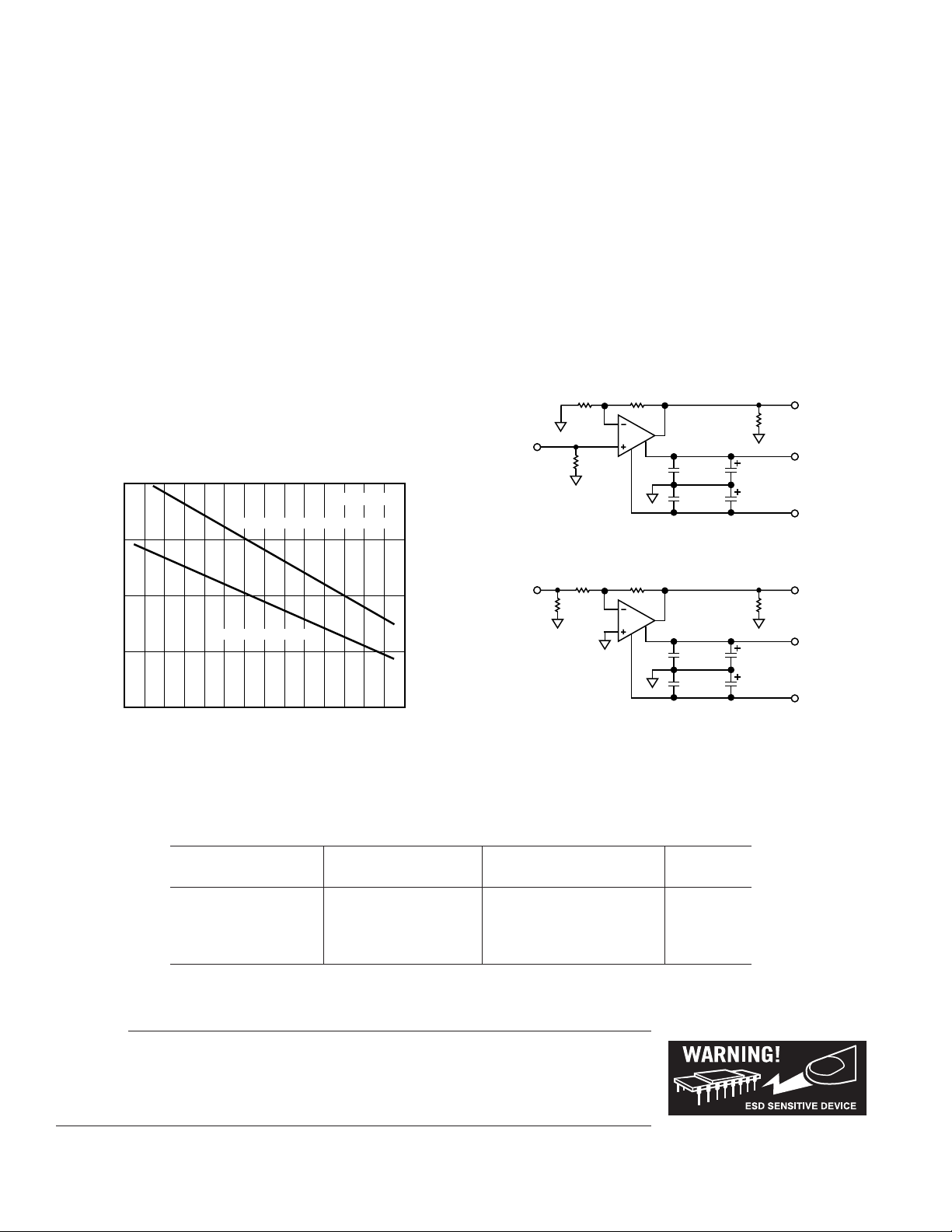
2.0
8-LEAD PLASTIC DIP PACKAGE
1.5
TJ = 150ⴗC
MAXIMUM POWER DISSIPATION
The maximum power that can be safely dissipated by the AD8011
is limited by the associated rise in junction temperature. The
maximum safe junction temperature for plastic encapsulated
devices is determined by the glass transition temperature of the
plastic, approximately 150°C. Exceeding this limit temporarily
may cause a shift in parametric performance due to a change in
the stresses exerted on the die by the package. Exceeding a
junction temperature of 175°C for an extended period can result
in device failure.
While the AD8011 is internally short-circuit protected, this may
not be sufficient to guarantee that the maximum junction temperature is not exceeded under all conditions. To ensure proper
operation, it is necessary to observe the maximum power derating
curves (shown in Figure 3).
1k⍀1k⍀
V
IN
50⍀
0.01F
0.01F
10F
10F
R
1k⍀
V
OUT
L
+V
S
–V
S
Figure 4. Test Circuit; Gain = +2
1.0
8-LEAD SOIC PACKAGE
0.5
MAXIMUM POWER DISSIPATION (W)
0
–50 –40 –30 –20 –10 0 10 20 30 40 50 60 70 80 90
AMBIENT TEMPERATURE (ⴗC)
V
IN
1k⍀
52.3⍀
Figure 5. Test Circuit; Gain = –1
1k⍀
0.01F
0.01F
Figure 3. Maximum Power Dissipation vs. Temperature
ORDERING GUIDE
Temperature Package Package
Model Range Description Option
AD8011AN –40°C to +85°C8-Lead PDIP N-8
AD8011AR –40°C to +85°C 8-Lead SOIC R-8
AD8011AR-REEL –40°C to +85°C 13" Tape and Reel R-8
AD8011AR-REEL7 –40°C to +85°C 7" Tape and Reel R-8
CAUTION
ESD (electrostatic discharge) sensitive device. Electrostatic charges as high as 4000 V readily
accumulate on the human body and test equipment and can discharge without detection. Although the
AD8011 features proprietary ESD protection circuitry, permanent damage may occur on devices
subjected to high energy electrostatic discharges. Therefore, proper ESD precautions are recommended
to avoid performance degradation or loss of functionality.
10F
10F
R
1k⍀
V
OUT
L
+V
S
–V
S
REV. C–4–
Typical Performance Characteristics–AD8011
(
)
(⍀)
20mV
5ns
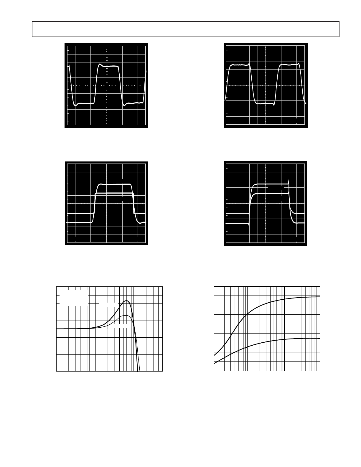
*TPC 1. 100 mV Step Response; G = +2,
= ±2.5 V or ±5 V
V
S
4V STEP
2V STEP
800mV
10ns
*TPC 2. Step Response; G = +2, VS = ±2.5 V
(2 V Step) and ±5 V (4 V Step)
6.5
G = +2
6.4
V
= 100mV p-p
IN
R
= 1k⍀
L
R
= 1k⍀
6.3
F
6.2
6.1
6.0
GAIN (dB)
5.9
5.8
5.7
5.6
5.5
1 10 100 500
VS = +5V
FREQUENCY
VS = ⴞ5V
MHz
TPC 3. Gain Flatness; G = +2
20mV
5ns
*TPC 4. 100 mV Step Response; G = –1,
= ±2.5 V or ±5 V
V
S
4V STEP
2V STEP
800mV
10ns
*TPC 5. Step Response; G = –1, VS = ±2.5 V
(2 V Step) and ±5 V (4 V Step)
9
8
7
6
5
4
SWING (V p-p)
3
2
1
0
10 100 1000 10000
LOAD RESISTANCE
ⴞ5V
+5V
TPC 6. Output Voltage Swing vs. Load
*NOTE: VS = ± 5 V operation is identical to VS = +5 V single-supply operation.
REV. C
–5–
 Loading...