

14-Bit, 8-Channel,
V
www.BDTIC.com/ADI
250 kSPS PulSAR ADC
FEATURES
14-bit resolution with no missing codes
8-channel multiplexer with choice of inputs
Unipolar single ended
Differential (GND sense)
Pseudobipolar
Throughput: 250 kSPS
INL/DNL: ±0.5 LSB typical
SINAD: 85 dB @ 20 kHz
THD: 100 dB @ 20 kHz
Analog input range: 0 V to V
with V
REF
up to VDD
REF
Multiple reference types
Internal selectable 2.5 V or 4.096 V
External buffered (up to 4.096 V)
External (up to VDD)
Internal temperature sensor
Channel sequencer, selectable 1-pole filter, busy indicator
No pipeline delay, SAR architecture
Single-supply 2.7 V to 5.5 V operation with
1.8
V to 5 V logic interface
Serial interface compatible with SPI, MICROWIRE,
SPI, and DSP
Q
Power dissipation
2.9 mW
@ 2.5 V/200 kSPS
10.8 mW @ 5 V/250 kSPS
Standby current: 50 nA
20-lead 4 mm × 4 mm LFCSP package
APPLICATIONS
Battery-powered equipment
Medical instruments: ECG/EKG
Mobile communications: GPS
Personal digital assistants
Power line monitoring
Data acquisition
Seismic data acquisition systems
Instrumentation
Process control
IN0
IN1
IN2
IN3
IN4
IN5
IN6
IN7
COM
Table 1. Multichannel 14-/16-Bit PulSAR® ADC
Type Channels 250 kSPS 500 kSPS ADC Driver
14-Bit 8 AD7949 ADA4841-x
16-Bit 4 AD7682 ADA4841-x
16-Bit 8 AD7689 AD7699 ADA4841-x
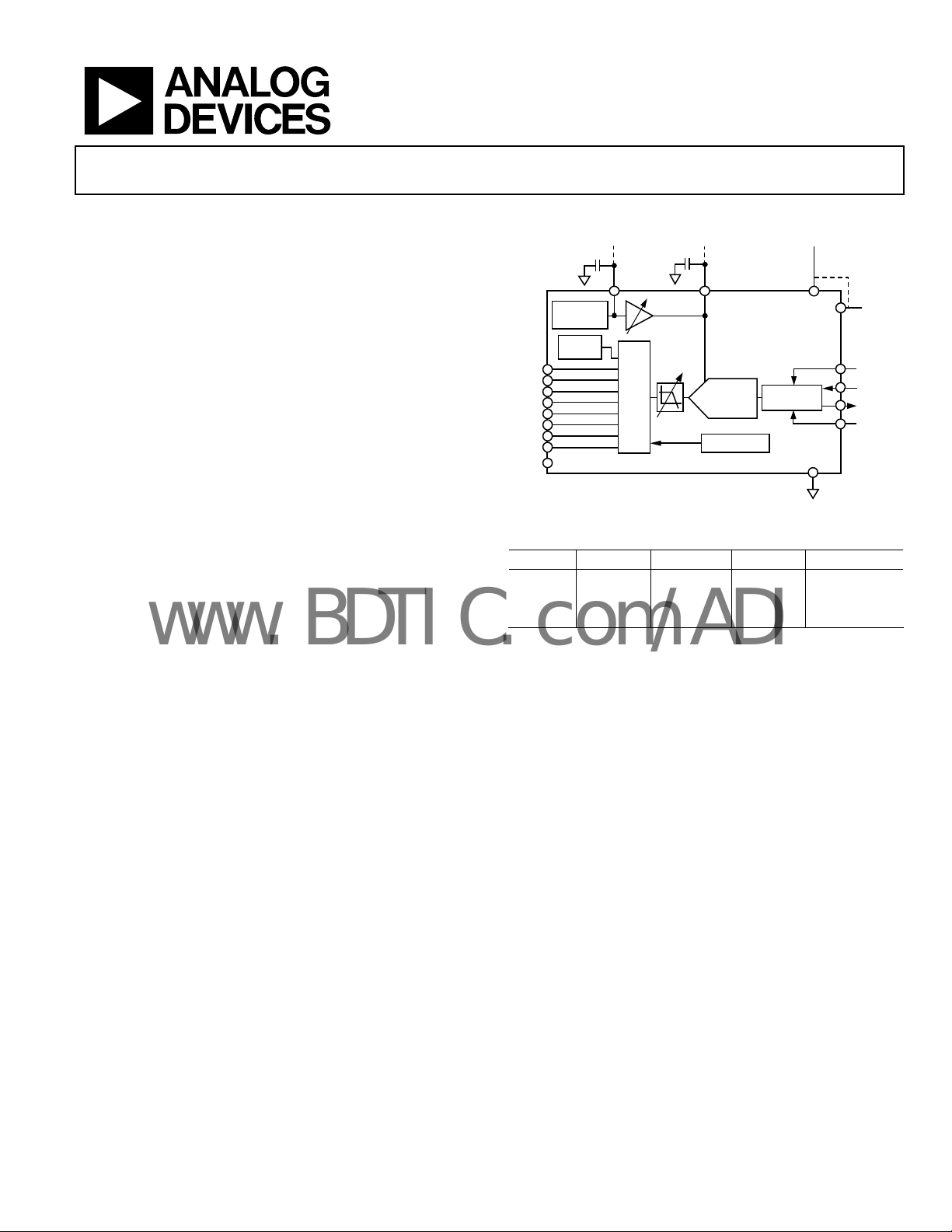
GENERAL DESCRIPTION
The AD7949 is an 8-channel, 14-bit, charge redistribution
successive approximation register (SAR) analog-to-digital
converter (ADC) that operates from a single power supply, VDD.
The AD7949 contains all components for use in a multichannel,
w power data acquisition system, including a true 14-bit SAR
lo
ADC with no missing codes; an 8-channel, low crosstalk multiplexer useful for configuring the inputs as single ended (with or
without ground sense), differential, or bipolar; an internal low
drift reference (selectable 2.5 V or 4.096 V) and buffer; a
temperature sensor; a selectable one-pole filter; and a sequencer
that is useful when channels are continuously scanned in order.
The AD7949 uses a simple SPI interface for writing to the
co
nfiguration register and receiving conversion results. The SPI
interface uses a separate supply, VIO, which is set to the host
logic level. Power dissipation scales with throughput.
The AD7949 is housed in a tiny 20-lead LFCSP with operation
s
pecified from −40°C to +85°C.
FUNCTIONAL BLOCK DIAGRAM
0.5V TO 4.096V
0.1µF
BAND GAP
REF
TEMP
SENSOR
REFIN
MUX
0.5V TO V DD
22µF
ONE-POLE
LPF
Figure 1.
REF
16-BIT SAR
ADC
SEQUENCER
AD7949
SPI SERIAL
INTERFACE
2.7V TO 5
VDD
GND
AD7949
1.8V
VIO
TO
VDD
CNV
SCK
SDO
DIN
07351-001
Rev. A
Information furnished by Analog Devices is believed to be accurate and reliable. However, no
responsibility is assumed by Anal og Devices for its use, nor for any infringements of patents or ot her
rights of third parties that may result from its use. Specifications subject to change without notice. No
license is granted by implication or otherwise under any patent or patent rights of Analog Devices.
Trademarks and registered trademarks are the property of their respective owners.
One Technology Way, P.O. Box 9106, Norwood, MA 02062-9106, U.S.A.
Tel: 781.329.4700 www.analog.com
Fax: 781.461.3113 ©2008 Analog Devices, Inc. All rights reserved.

AD7949
www.BDTIC.com/ADI
TABLE OF CONTENTS
Features .............................................................................................. 1
Applications....................................................................................... 1
Functional Block Diagram .............................................................. 1
General Description......................................................................... 1
Revision History ............................................................................... 2
Specifications..................................................................................... 3
Timing Specifications....................................................................... 6
Absolute Maximum Ratings............................................................ 8
ESD Caution.................................................................................. 8
Pin Configuration and Function Descriptions............................. 9
Typical Performance Characteristics ........................................... 10
Te r mi n ol o g y .................................................................................... 13
Theory of Operation ...................................................................... 14
Overview...................................................................................... 14
Converter Operation.................................................................. 14
Transf e r Fu ncti o ns ...................................................................... 15
Typical C o n ne ction D i a g rams .................................................. 16
Analog Inputs ............................................................................. 17
Driver Amplifier Choice ........................................................... 18
Voltage Reference Output/Input .............................................. 19
Power Supply............................................................................... 20
Supplying the ADC from the Reference.................................. 20
Digital Interface .............................................................................. 21
Configuration Register, CFG.................................................... 22
Read/Write Spanning Conversion Without a
Busy Indicator............................................................................. 23
Read/Write Spanning Conversion with a Busy Indicator..... 24
Application Hints ........................................................................... 25
Layout .......................................................................................... 25
Evaluating AD7949 Performance............................................. 25
Outline Dimensions ....................................................................... 26
Ordering Guide .......................................................................... 26
REVISION HISTORY
5/08—Rev. 0 to Rev. A
Changes to Ordering Guide.......................................................... 26
5/08—Revision 0: Initial Version
Rev. A | Page 2 of 28
AD7949
www.BDTIC.com/ADI
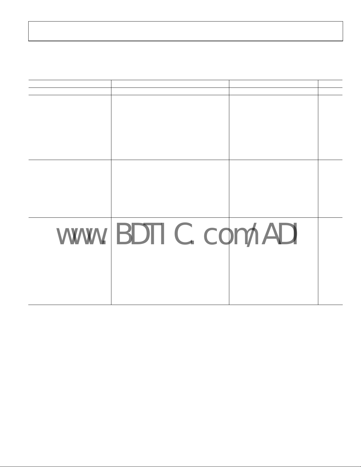
SPECIFICATIONS
VDD = 2.5 V to 5.5 V, VIO = 2.3 V to VDD, V
Table 2.
Parameter Conditions/Comments Min Typ Max Unit
RESOLUTION 14 Bits
ANALOG INPUT
Voltage Range Unipolar mode 0 +V
Bipolar mode −V
Absolute Input Voltage Positive input, unipolar and bipolar modes −0.1 V
Negative or COM input, unipolar mode −0.1 +0.1
Negative or COM input, bipolar mode V
Analog Input CMRR fIN = 250 kHz 68 dB
Leakage Current at 25°C Acquisition phase 1 nA
Input Impedance
1
THROUGHPUT
Conversion Rate
Full Bandwidth
2
VDD = 4.5 V to 5.5 V 0 250 kSPS
VDD = 2.3 V to 4.5 V 0 200 kSPS
¼ Bandwidth
2
VDD = 4.5 V to 5.5 V 0 62.5 kSPS
VDD = 2.3 V to 4.5 V 0 50 kSPS
Transient Response Full-scale step, full bandwidth 1.8 s
Full-scale step, ¼ bandwidth 14.8 s
ACCURACY
No Missing Codes 14 Bits
Integral Linearity Error −1 ±0.5 +1 LSB
Differential Linearity Error −1 ±0.25 +1 LSB
Transition Noise REF = VDD = 5 V 0.1 LSB
Gain Error
4
−5 ±0.5 +5 LSB
Gain Error Match −1 ±0.2 +1 LSB
Gain Error Temperature Drift ±1 ppm/°C
Offset Error
4
±0.5 LSB
Offset Error Match −1 ±0.2 +1 LSB
Offset Error Temperature Drift ±1 ppm/°C
Power Supply Sensitivity
VDD = 5 V ± 5%
= VDD, all specifications T
REF
MIN
to T
, unless otherwise noted.
MAX
V
3
/2 +V
REF
/2 − 0.1 V
REF
/2 V
REF
REF
/2
REF
+ 0.1 V
REF
/2 + 0.1
REF
±0.2 LSB
Rev. A | Page 3 of 28

AD7949
www.BDTIC.com/ADI
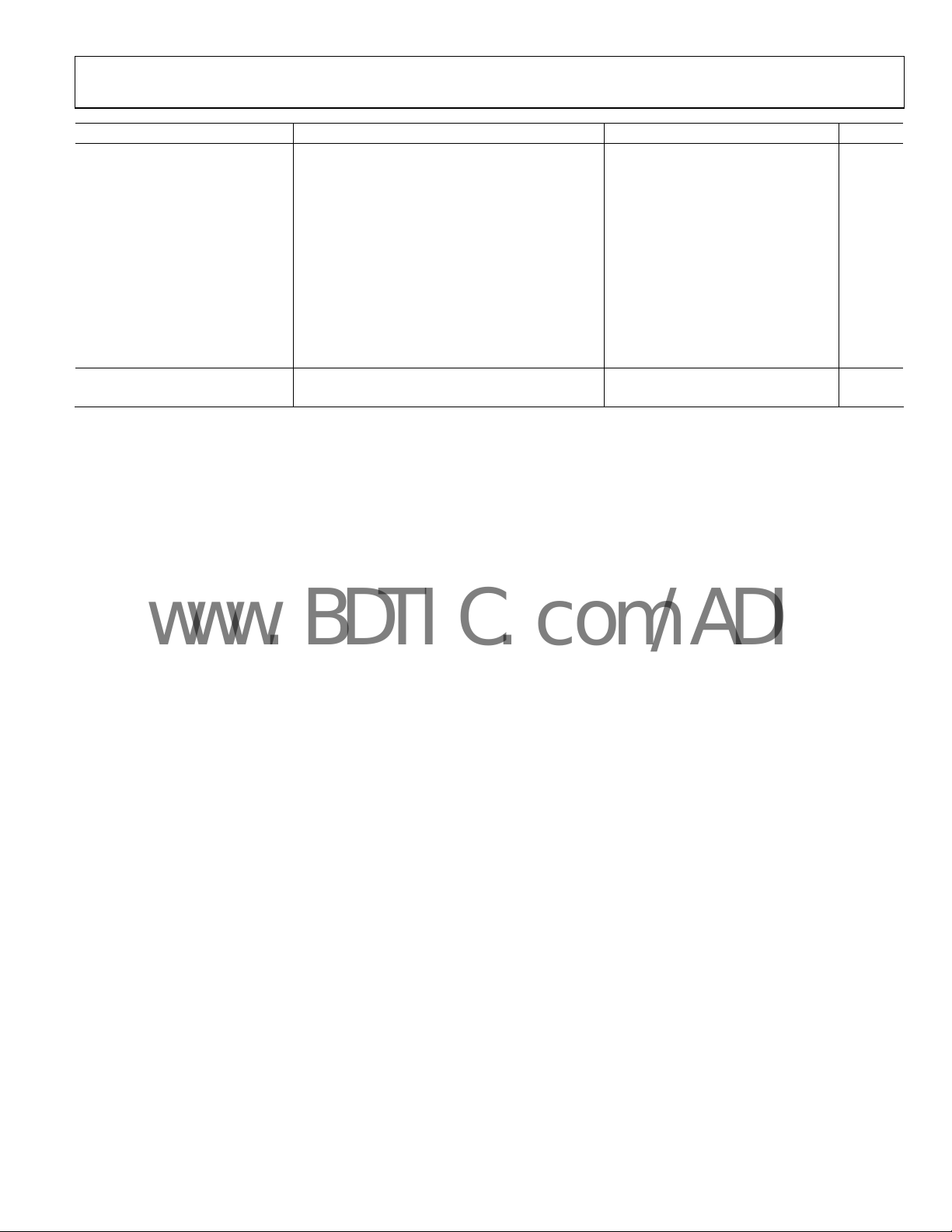
Parameter Conditions/Comments Min Typ Max Unit
AC ACCURACY
Dynamic Range 85.6 dB
Signal-to-Noise fIN = 20 kHz, VREF = 5 V 84.5 85.5 dB
f
f
SINAD fIN = 20 kHz, VREF = 5 V 84 85 dB
f
f
f
Total Harmonic Distortion fIN = 20 kHz −100 dB
Spurious-Free Dynamic Range fIN = 20 kHz 108 dB
Channel-to-Channel Crosstalk fIN = 100 kHz on adjacent channel(s) −125 dB
SAMPLING DYNAMICS
−3 dB Input Bandwidth Selectable 0.425 1.7 MHz
Aperture Delay VDD = 5 V 2.5 ns
INTERNAL REFERENCE
REF Output Voltage 2.5 V, @ 25°C 2.490 2.500 2.510 V
4.096 V, @ 25°C 4.086 4.096 4.106 V
REFIN Output Voltage
4.096 V, @ 25°C 2.3 V
REF Output Current ±300 µA
Temperature Drift ±10 ppm/°C
Line Regulation VDD = 5 V ± 5% ±15 ppm/V
Long-Term Drift 1000 hours 50 ppm
Turn-On Settling Time CREF = 10 µF 5 ms
EXTERNAL REFERENCE
Voltage Range REF input 0.5 VDD + 0.3 V
REFIN input (buffered) 0.5 VDD − 0.2 V
Current Drain 250 kSPS, REF = 5 V 50 µA
TEMPERATURE SENSOR
Output Voltage
Temperature Sensitivity 1 mV/°C
DIGITAL INPUTS
Logic Levels
V
IL
V
IH
I
IL
I
IH
DIGITAL OUTPUTS
Data Format
Pipeline Delay
V
OL
V
OH
5
7
8
6
= 20 kHz, VREF = 4.096 V internal REF 85 dB
IN
= 20 kHz, VREF = 2.5 V internal REF 84 dB
IN
= 20 kHz, VREF = 5 V, −60 dB input 33.5 dB
IN
= 20 kHz, VREF = 4.096 V internal REF 85 dB
IN
= 20 kHz, VREF = 2.5 V internal REF 84 dB
IN
2.5 V, @ 25°C 1.2 V
@ 25°C 283 mV
−0.3 +0.3 × VIO V
0.7 × VIO VIO + 0.3 V
−1 +1 µA
−1 +1 µA
9
10
ISINK = +500 µA 0.4 V
ISOURCE = −500 µA VIO − 0.3 V
Rev. A | Page 4 of 28
AD7949
www.BDTIC.com/ADI
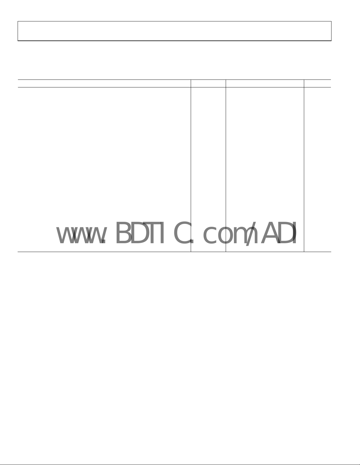
Parameter Conditions/Comments Min Typ Max Unit
POWER SUPPLIES
VDD Specified performance 2.3 5.5 V
VIO Specified performance 2.3 VDD + 0.3 V
Operating range 1.8 VDD + 0.3 V
Standby Current
Power Dissipation VDD = 2.5 V, 100 SPS throughput 1.5 µW
VDD = 2.5V, 100 kSPS throughput 1.45 2.0 mW
VDD = 2.5 V, 200 kSPS throughput 2.9 4.0 mW
VDD = 5 V , 250 kSPS throughput 10.8 12.5 mW
Energy per Conversion 50 nJ
TEMPERATURE RANGE
Specified Performance T
1
See the Analog Inputs section.
2
The bandwidth is set with the configuration register
3
LSB means least significant bit. With the 5 V input range, one LSB = 305 µV.
4
See the Terminology section. These specifications include full temperature range variation but not the error contribution from the external reference.
5
With VDD = 5 V, unless otherwise noted.
6
All specifications expressed in decibels are referred to a full-scale input FSR and tested with an input signal at 0.5 dB below full scale, unless otherwise specified.
7
This is the output from the internal band gap.
8
The output voltage is internal and present on a dedicated multiplexer input.
9
Unipolar mode: serial 14-bit straight binary.
Bipolar mode: serial 14-bit twos complement.
10
Conversion results available immediately after completed conversion.
11
With all digital inputs forced to VIO or GND as required.
12
During acquisition phase.
13
Contact an Analog Devices, Inc., sales representative for the extended temperature range.
11, 12
VDD and VIO = 5 V, @ 25°C 50 nA
VDD = 5 V, 250 kSPS throughput with internal
ference
re
13
to T
MIN
MAX
13.5 15.5 mW
−40 +85 °C
Rev. A | Page 5 of 28
AD7949
www.BDTIC.com/ADI
TIMING SPECIFICATIONS
VDD = 4.5 V to 5.5 V, VIO = 2.3 V to VDD, all specifications T
Table 3.
1
Parameter Symbol Min Typ Max Unit
Conversion Time: CNV Rising Edge to Data Available t
Acquisition Time t
Time Between Conversions t
CNV Pulse Width t
Data Write/Read During Conversion t
SCK Period t
SCK Low Time t
SCK High Time t
SCK Falling Edge to Data Remains Valid t
SCK Falling Edge to Data Valid Delay t
VIO Above 4.5 V 16 ns
VIO Above 3 V 17 ns
VIO Above 2.7 V 18 ns
VIO Above 2.3 V 19 ns
CNV Low to SDO D15 MSB Valid t
VIO Above 4.5 V 15 ns
VIO Above 3 V 17 ns
VIO Above 2.7 V 18 ns
VIO Above 2.3 V 22 ns
CNV High or Last SCK Falling Edge to SDO High Impedance t
CNV Low to SCK Rising Edge t
DIN Valid Setup Time from SCK Falling Edge t
DIN Valid Hold Time from SCK Falling Edge t
1
See Figure 2 and Figure 3 for load conditions.
MIN
to T
, unless otherwise noted.
MAX
CONV
ACQ
CYC
CNVH
DATA
SCK
SCKL
SCKH
HSDO
DSDO
EN
DIS
CLSCK
SDIN
HDIN
2.2 µs
1.8 µs
4 µs
10 ns
1.0 µs
15 ns
7 ns
7 ns
4 ns
25 ns
10 ns
4 ns
4 ns
Rev. A | Page 6 of 28
AD7949
T
3
www.BDTIC.com/ADI
VDD = 2.3 V to 4.5 V, VIO = 2.3 V to VDD, all specifications T
Table 4.
1
Parameter Symbol Min Typ Max Unit
Conversion Time: CNV Rising Edge to Data Available t
Acquisition Time t
Time Between Conversions t
CNV Pulse Width t
Data Write/Read During Conversion t
SCK Period t
SCK Low Time t
SCK High Time t
SCK Falling Edge to Data Remains Valid t
SCK Falling Edge to Data Valid Delay t
VIO Above 3 V 24 ns
VIO Above 2.7 V 30 ns
VIO Above 2.3 V 37 ns
CNV Low to SDO D15 MSB Valid t
VIO Above 3 V 21 ns
VIO Above 2.7 V 27 ns
VIO Above 2.3 V 35 ns
CNV High or Last SCK Falling Edge to SDO High Impedance t
CNV Low to SCK Rising Edge t
SDI Valid Setup Time from SCK Falling Edge t
SDI Valid Hold Time from SCK Falling Edge t
1
See Figure 2 and Figure 3 for load conditions.
MIN
to T
, unless otherwise noted.
MAX
CONV
ACQ
CYC
CNVH
DATA
SCK
SCKL
SCKH
HSDO
DSDO
EN
DIS
CLSCK
SDIN
HDIN
3.2 µs
1.8 µs
5 µs
10 ns
1.0 µs
25 ns
12 ns
12 ns
5 ns
50 ns
10 ns
5 ns
5 ns
500µA
OSDO
50pF
C
L
500µA
Figure 2. Load Circuit for Di
I
OL
1.4V
I
OH
07351-002
gital Interface Timing
0% VIO
t
DELAY
2V OR VIO – 0.5V
0.8V OR 0.5V
1
2V IF VI O ABOVE 2. 5V, VIO – 0.5V IF VIO BEL OW 2.5V.
2
0.8V IF VIO ABOV E 2.5V, 0. 5V IF V IO BELO W 2.5V.
2
Figure 3. Voltage Levels for Timing
70% VIO
t
DELAY
1
2V OR VIO – 0.5V
0.8V OR 0.5V
1
2
07351-003
Rev. A | Page 7 of 28
AD7949
www.BDTIC.com/ADI
ABSOLUTE MAXIMUM RATINGS
Table 5.
Parameter Rating
Analog Inputs
INx,1 COM
REF, REFIN GND − 0.3 V to VDD + 0.3 V
Supply Voltages
VDD, VIO to GND −0.3 V to +7 V
VDD to VIO ±7 V
DIN, CNV, SCK to GND2 −0.3 V to VIO + 0.3 V
SDO to GND −0.3 V to VIO + 0.3 V
Storage Temperature Range −65°C to +150°C
Junction Temperature 150°C
θJA Thermal Impedance (LFCSP) 47.6°C/W
θJC Thermal Impedance (LFCSP) 4.4°C/ W
1
See the Analog Inputs section.
2
CNV must be low during power up. See the Power Supply section.
1
GND − 0.3 V to VDD + 0.3 V
or VDD ± 130 mA
Stresses above those listed under Absolute Maximum Ratings
may cause permanent damage to the device. This is a stress
rating only; functional operation of the device at these or any
other conditions above those indicated in the operational
section of this specification is not implied. Exposure to absolute
maximum rating conditions for extended periods may affect
device reliability.
ESD CAUTION
Rev. A | Page 8 of 28
AD7949
www.BDTIC.com/ADI
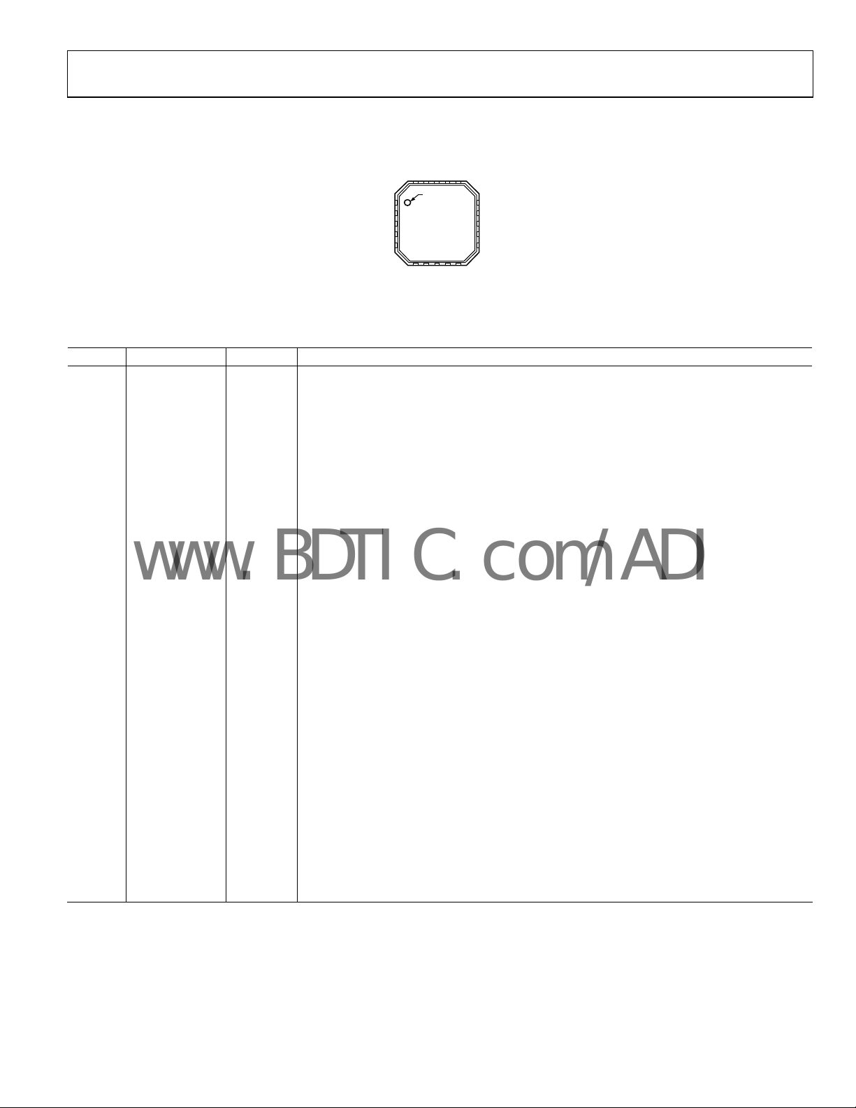
PIN CONFIGURATION AND FUNCTION DESCRIPTIONS
0
IN2
IN3
VDD
IN1
IN
71
61
81
91
02
PIN 1
INDICATOR
1VDD
2REF
AD7949
3REFIN
4GND
TOP VIEW
5GND
(Not to Scale)
8
6
7
IN4
IN5
IN6
Figure 4. 20-Lead LFCSP Pin Configuration
15 VIO
14 SDO
13 SCK
12 DIN
11 CNV
01
9
IN7
COM
07351-004
Table 6. Pin Function Descriptions
Pin No. Mnemonic Type
1, 20 VDD P
1
Description
Power Supply. Nominally 2.5 V to 5.5 V when using an ex
10 F and 100 nF capacitors.
When using the internal reference for 2.5 V outp
When using the internal reference for 4.096 V output, the minimum should be 4.5 V.
2 REF AI/O
Reference Input/Output. See the Voltage Reference Output/Input section.
the internal reference is enabled, this pin produces a selectable system reference = 2.5 V or
When
4.096 V.
When the internal reference is disabled and the buffer is enabled, REF produces a buffered
version of the voltage present on the REFIN pin (4.096 V maximum) useful when using low cost,
low power references.
For improved drift performance, connect a precision reference to REF (0.5 V to VDD).
For any reference method, this pin needs decoupling with an external 10 F capacitor
connected as close to REF as possible. See the
3 REFIN AI/O
Internal Reference Output/Reference Buffer Input. See the Voltage Reference Output/Input
tion.
sec
When using the internal reference, the internal unbuffered reference voltage is present and
s decoupling with a 0.1F capacitor.
need
When using the internal reference buffer, apply a source between 0.5 V and 4.096 V that is
buffered to the REF pin as described above.
4, 5 GND P Power Supply Ground.
6 to 9 IN4 to IN7 AI Channel 4 through Channel 7 Analog Inputs.
10 COM AI
11 CNV DI
12 DIN DI
Common Channel Input. All channels [7:0] can be referenced to a common mode point of 0 V or
V
/2 V.
REF
Convert Input. On the rising edge, CNV initiates the conversion. During conversion, if CNV is
high, the busy indictor is enabled.
held
Data Input. This input is used f
or writing to the 14-bit configuration register. The configuration
register can be written to during and after conversion.
13 SCK DI
Serial Data Clock Input. This input is used t
o clock out the data on ADO and clock in data on DIN
in an MSB first fashion.
14 SDO DO
Serial Data Output. The conversion r
esult is output on this pin synchronized to SCK. In unipolar
modes, conversion results are straight binary; in bipolar modes, conversion results are twos
complement.
15 VIO P
Input/Output Interface Digital Power. Nominally at the same supply as the host interface (1.8 V,
V, 3 V, or 5 V).
2.5
16 to 19 IN0 to IN3 AI Channel 0 through Channel 3 Analog Inputs.
1
AI = analog input, AI/O = analog input/output, DI = digital input, DO = digital output, and P = power.
ternal reference and decoupled with
ut, the minimum should be 3.0 V.
Reference Decoupling section.
Rev. A | Page 9 of 28

AD7949
www.BDTIC.com/ADI
TYPICAL PERFORMANCE CHARACTERISTICS
VDD = 2.5 V to 5.5 V, VREF = 2.5 V to 5 V, VIO = 2.3 V to VDD
1.0
1.0
0.5
0
INL (LSB)
–0.5
–1.0
0 4,096 8,192
CODES
12,288 16,384
Figure 5. Integral Nonlinearity vs. Code, VREF = VDD = 5 V
300k
261,120
250k
200k
150k
COUNTS
100k
50k
00010000
0
1FFD 1FFE 1FFF 2000 2001 2002 2003
1FFC
CODE IN HEX
V
REF
Figure 6. Histogram of a DC Input at Code Center
0
–20
–40
–60
–80
–100
–120
AMPLITUDE (dB of Full-Scale)
–140
–160
05025 75 100 125
V
= VDD = 5V
REF
f
= 250kSPS
S
f
= 19.9kHz
IN
SNR = 85.3dB
SINAD = 85.2dB
THD = –100dB
SFDR = 103dB
SECOND HARMONIC = –110dB
THIRD HARMONI C = –103dB
FREQUENCY (kHz)
Figure 7. 20 kHz FFT, VREF = VDD = 5 V
= VDD = 5V
0.5
0
DNL (LS B)
–0.5
–1.0
0 4,096 8,192
07351-006
CODES
Figure 8. Differential Nonlinearity vs. Code, VREF =
300k
259,473
250k
200k
150k
COUNTS
100k
50k
00 0
0
1FFD 1FFE 1FFF 2000 2001 2002 2003 2004
07351-007
1FFC
955 693
CODE IN HEX
12,288 16,384
VDD = 5 V
V
= VDD = 2.5V
REF
000
07351-009
07351-010
Figure 9. Histogram of a DC Input at Code Center
0
–20
–40
–60
–80
–100
–120
–140
AMPLITUDE ( dB of Full-Scal e)
–160
–180
05025 75 100
07351-008
V
= VDD = 2.5V
REF
f
= 200kSPS
s
f
= 19.9kHz
IN
SNR = 84.2dB
SINAD = 82.4dB
THD = –84dB
SFDR = 85dB
SECOND HARMONIC = –100dB
THIRD HARMONIC = –85dB
FREQUENCY (kHz)
07351-011
Figure 10. 20 kHz FFT, VREF = VDD = 2.5 V
Rev. A | Page 10 of 28

AD7949
–
–
www.BDTIC.com/ADI
90
90
85
80
75
SNR (dB)
70
65
60
VDD = V
VDD = V
VDD = V
VDD = V
0 50 100 150 200
= 5V, –0.5d B
REF
= 5V, –10dB
REF
= 2.5V, –0. 5dB
REF
= 2.5V, –10d B
REF
FREQUENCY (kHz)
Figure 11. SNR vs. Frequency
88
SNR
SINAD
ENOB
86
84
82
SNR, SINAD (dB)
80
78
1.5 2.0 2.5 3.0 3.5 4.0 4.5 5.0 5. 5
1.0
REFERENCE VOL TAGE (V)
Figure 12. SNR, SINAD, and ENOB vs. Reference Voltage
90
f
= 20kHz
IN
85
80
75
SNR (dB)
70
65
VDD = V
VDD = V
REF
REF
= 5V
= 2.5V
15.5
15.0
14.5
14.0
13.5
13.0
85
80
75
SINAD (dB)
70
65
60
07351-041
VDD = V
VDD = V
VDD = V
VDD = V
0 50 100 150 200
= 5V, –0.5d B
REF
= 5V, –10dB
REF
= 2.5V, –0. 5dB
REF
= 2.5V, –10d B
REF
FREQUENCY (kHz)
07351-012
Figure 14. SINAD vs. Frequency
130
125
120
115
110
105
100
95
ENOB (Bits)
07351-013
SFDR (dB)
70
90
85
80
75
1.5 2.0 2.5 3.0 3.5 4.0 4.5 5.0 5.5
1.0
REFERENCE VOL TAGE (V)
SFDR
THD
60
–65
–70
–75
–80
–85
–90
–95
–100
–105
–110
–115
–120
THD (dB)
07351-016
Figure 15. SFDR and THD vs. Reference Voltage
90
f
= 20kHz
IN
–95
–100
THD (dB)
–105
VDD = V
VDD = V
REF
REF
= 2.5V
= 5V
60
–35 –15 5 25 45 65 85 105
–55
TEMPERATURE (° C)
Figure 13. SNR vs. Temperature
125
07351-014
–110
–35 –15 5 25 45 65 85 105
–55
Figure 16. THD vs. Temperature
Rev. A | Page 11 of 28
TEMPERATURE (° C)
125
07351-017

AD7949
–
A
www.BDTIC.com/ADI
60
–70
–80
2750
2500
2250
2000
2.5V INTERNAL REF
4.096V INTERNAL REF
INTERNAL BUFFER, TEMP ON
INTERNAL BUFFER, TEMP OFF
EXTERNAL REF, TEMP ON
EXTERNAL REF, TEMP OFF
VIO
f
= 200kSPS
S
100
90
80
70
–90
THD (dB)
–100
VDD = V
–110
–120
0 50 100 150 200
FREQUENCY (kHz)
VDD = V
VDD = V
VDD = V
= 5V, –0.5d B
REF
= 2.5V, –0.5d B
REF
= 2.5V, –10dB
REF
= 5V, –10dB
REF
Figure 17. THD vs. Frequency
90
f
= 20kHz
IN
89
88
87
86
85
84
SNR (dB)
83
82
81
80
79
78
–10
VDD = V
VDD = V
–8 –6 –2 0–4
= 5V
REF
= 2.5V
REF
INPUT LEVEL (dB)
Figure 18. SNR vs. Input Level Figure 21. Operating Currents vs. Temperature
2
1750
1500
VDD CURRENT (µA)
1250
1000
750
2.5 3.0 3.5 4.0 4. 5 5.0 5.5
07351-015
VDD SUPPLY (V)
60
50
VIO CURRENT (µ A)
40
30
20
07351-021
Figure 20. Operating Currents vs. Supply
3000
f
= 200kSPS
S
2750
2500
VDD = 5V, INTERNAL 4.096V REF
2250
2000
1750
VDD CURRENT (µA)
1500
1250
1000
07351-018
VDD = 5V, EXTERNAL REF
VDD = 2.5, EXTERNAL REF
–55
–35 –15 5 25 45 65 85 105
25
TEMPERATURE (° C)
VIO
125
180
160
140
120
100
80
60
40
20
07351-022
1
0
–1
OFFSET ERROR AND GAIN ERRO R (LSB)
–2
–55
UNIPOLAR ZERO
UNIPOLAR GAI N
BIPOLAR ZERO
BIPOLAR GAIN
–35 –15 5 25 45 65 85 105
TEMPERATURE (° C)
Figure 19. Offset and Gain Errors vs. Temperature
125
20
15
Y (ns)
DEL
10
DSDO
T
5
0
07351-020
Figure 22. t
VDD = 2.5V, 25°C
VDD = 3.3V, 25°C
Delay vs. SDO Capacitance Load and Supply
DSDO
VDD = 2.5V, 85°C
VDD = 3.3V, 85°C
SDO CAPACITIVE LOAD (pF)
VDD = 5V, 25°C
VDD = 5V, 85°C
1200 20406080100
7351-023
Rev. A | Page 12 of 28

AD7949
www.BDTIC.com/ADI
TERMINOLOGY
Least Significant Bit (LSB)
The LSB is the smallest increment that can be represented by a
c
onverter. For an analog-to-digital converter with N bits of
resolution, the LSB expressed in volts is
V
REF
LSB2(V) =
N
Integral Nonlinearity Error (INL)
INL refers to the deviation of each individual code from a line
wn from negative full scale through positive full scale. The
dra
point used as negative full scale occurs ½ LSB before the first
code transition. Positive full scale is defined as a level 1½ LSB
beyond the last code transition. The deviation is measured from
the middle of each code to the true straight line (see
Figure 24).
Differential Nonlinearity Error (DNL)
In an ideal ADC, code transitions are 1 LSB apart. DNL is the
um deviation from this ideal value. It is often specified in
maxim
terms of resolution for which no missing codes are guaranteed.
Offset Error
The first transition should occur at a level ½ LSB above analog
round. The unipolar offset error is the deviation of the actual
g
transition from that point.
Gain Error
The last transition (from 111 … 10 to 111 … 11) should occur
or an analog voltage 1½ LSB below the nominal full scale. The
f
gain error is the deviation in LSB (or percentage of full-scale
range) of the actual level of the last transition from the ideal
level after the offset error is adjusted out. Closely related is the
full-scale error (also in LSB or percentage of full-scale range),
which includes the effects of the offset error.
Aperture Delay
Aperture delay is the measure of the acquisition performance. It
is t
he time between the rising edge of the CNV input and the
point at which the input signal is held for a conversion.
Transi ent Res p ons e
Transient response is the time required for the ADC to accurately
acq
uire its input after a full-scale step function is applied.
Dynamic Range
Dynamic range is the ratio of the rms value of the full scale to
e total rms noise measured with the inputs shorted together.
th
The value for dynamic range is expressed in decibels.
Signal-to-Noise Ratio (SNR)
SNR is the ratio of the rms value of the actual input signal to the
r
ms sum of all other spectral components below the Nyquist
frequency, excluding harmonics and dc. The value for SNR is
expressed in decibels.
Signal-to-(Noise + Distortion) Ratio (SINAD)
SINAD is the ratio of the rms value of the actual input signal to
he rms sum of all other spectral components below the Nyquist
t
frequency, including harmonics but excluding dc. The value for
SINAD is expressed in decibels.
Total Harmonic Distortion (THD)
THD is the ratio of the rms sum of the first five harmonic
co
mponents to the rms value of a full-scale input signal and is
expressed in decibels.
Spurious-Free Dynamic Range (SFDR)
SFDR is the difference, in decibels, between the rms amplitude
o
f the input signal and the peak spurious signal.
Effective Number of Bits (ENOB)
ENOB is a measurement of the resolution with a sine wave
in
put. It is related to SINAD by the formula
ENOB = (SINA
− 1.76)/6.02
D
dB
and is expressed in bits.
Channel-to-Channel Crosstalk
Channel-to-channel crosstalk is a measure of the level of
cr
osstalk between any two adjacent channels. It is measured by
applying a dc to the channel under test and applying a full-scale,
100 kHz sine wave signal to the adjacent channel(s). The
crosstalk is the amount of signal that leaks into the test channel
and is expressed in decibels.
Reference Voltage Temperature Coefficient
Reference voltage temperature coefficient is derived from the
t
ypical shift of output voltage at 25°C on a sample of parts at the
maximum and minimum reference output voltage (V ) measured at T , T (25°C), and T . It is expressed in ppm/°C as
MIN MAX
TCV
REF
)Cppm/( ×
MinVMaxV
)(–)(
=°
REF
REFREF
×°
MAX
10
TTV
)–()C25(
MIN
where:
V
(Max) = maximum V
REF
(Min) = minimum V
V
REF
V
(25°C) = V
REF
= +85°C.
T
MAX
T
= –40°C.
MIN
at 25°C.
REF
REF
REF
at T
at T
MIN
MIN
, T (25°C), or T
, T (25°C), or T
MAX
MAX
REF
6
.
.
Rev. A | Page 13 of 28

AD7949
www.BDTIC.com/ADI
THEORY OF OPERATION
INx+
REF
GND
INx– OR
COM
4,096C
4,096C
4C 2C C C8,192C
4C 2C C C8,192C
Figure 23. ADC Simplified Schematic
LSB
LSB
SWITCHES CONTROL
SW+MSB
COMP
SW–MSB
CONTROL
LOGIC
CNV
BUSY
OUTPUT CO DE
07351-026
OVERVIEW
The AD7949 is an 8-channel, 14-bit, charge redistribution
successive approximation register (SAR) analog-to-digital
converter (ADC). The AD7949 is capable of converting 250,000
samples per second (250 kSPS) and powers down between
conversions. For example, when operating with an external
reference at 1 kSPS, it consumes 15 µW typically, ideal for
battery-powered applications.
The AD7949 contains all of the components for use in a multi-
nnel, low power, data acquisition system, including
cha
• 14-b
• 8
• I
• Te
• S
• C
These components are configured through an SPI-compatible,
14-b
read after or during conversions with the option for reading
back the current configuration.
The AD7949 provides the user with an on-chip track-and-hold
a
nd does not exhibit pipeline delay or latency.
The AD7949 is specified from 2.3 V to 5.5 V and can be
in
a 20-lead, 4 mm × 4 mm LFCSP that combines space savings
and allows flexible configurations. It is pin-for-pin compatible
with the 16-bit
it SAR ADC with no missing codes
-channel, low crosstalk multiplexer
nternal low drift reference and buffer
mpe r atu r e s e ns o r
electable one-pole filter
hannel sequencer
it register. Conversion results, also SPI compatible, can be
terfaced to any 1.8 V to 5 V digital logic family. It is housed in
AD7682, AD7699, and AD7689.
CONVERTER OPERATION
The AD7949 is a successive approximation ADC based on a
charge redistribution DAC. Figure 23 shows the simplified
chematic of the ADC. The capacitive DAC consists of two
s
identical arrays of 14 binary-weighted capacitors, which are
connected to the two comparator inputs.
During the acquisition phase, terminals of the array tied to the
c
omparator input are connected to GND via SW+ and SW−. All
independent switches are connected to the analog inputs.
Thus, the capacitor arrays are used as sampling capacitors and
uire the analog signal on the INx+ and INx− (or COM)
acq
inputs. When the acquisition phase is complete and the CNV
input goes high, a conversion phase is initiated. When the
conversion phase begins, SW+ and SW− are opened first. The
two capacitor arrays are then disconnected from the inputs and
connected to the GND input. Therefore, the differential voltage
between the INx+ and INx− (or COM) inputs captured at the
end of the acquisition phase is applied to the comparator inputs,
causing the comparator to become unbalanced. By switching
each element of the capacitor array between GND and CAP, the
comparator input varies by binary-weighted voltage steps
(V
/2, V
REF
/4, ... V
REF
switches, starting with the MSB, to bring the comparator back
into a balanced condition. After the completion of this process,
the part returns to the acquisition phase, and the control logic
generates the ADC output code and a busy signal indicator.
Because the AD7949 has an on-board conversion clock, the
erial clock, SCK, is not required for the conversion process.
s
/16,384). The control logic toggles these
REF
Rev. A | Page 14 of 28

AD7949
www.BDTIC.com/ADI
TRANSFER FUNCTIONS
With the inputs configured for unipolar range (single ended,
COM with ground sense, or paired differentially with INx− as
ground sense), the data output is straight binary.
With the inputs configured for bipolar range (COM = V
paired differentially with INx− = V
/2), the data outputs are
REF
twos complement.
The ideal transfer characteristic for the AD7949 is shown in
Figure 24 and for both unipolar and bipolar ranges with the
in
ternal 4.096 V reference.
REF
/2 or
TWOS
COMPLEMENT
011...111
011...110
011...101
ADC CODE
100...010
100...001
100...000
STRAIGHT
BINARY
111...111
111...110
111...101
000...010
000...001
000...000
–FSR
–FSR + 1LSB
–FSR + 0.5L SB
ANALOG INPUT
Figure 24. ADC Ideal Transfer Function
+FSR – 1.5L SB
+FSR – 1LSB
07351-027
Table 7. Output Codes and Ideal Input Voltages
Description
Unipolar Analog Input
= 4.096 V
V
REF
1
Digital Output Code
(S
traight Binary Hex)
Bipolar Analog Input
= 4.096 V
V
REF
2
Digital Output Code
(
Twos Complement Hex)
FSR − 1 LSB 4.095750 V 0x3FFF 2.047750 V 0x1FFF
Midscale + 1 LSB 2.048250 V 0x2001 250 V 0x0001
Midscale 2.048 V 0x2000 0
0x0000
Midscale − 1 LSB 2.04775 V 0x1FFF −250 V 0x3FFF
−FSR + 1 LSB 250 V 0x0001 −2.047750 V 0x2001
−FSR 0 V 0x0000 −2.048 V 0x2000
1
With COM or INx− = 0 V or all INx referenced to GND.
2
With COM or INx− = V
3
This is also the code for an overranged analog input ((INx+) − (INx−), or COM, above V
4
This is also the code for an underranged analog input ((INx+) − (INx−), or COM, below V
/2.
REF
− V
).
REF
GND
).
GND
4
3
Rev. A | Page 15 of 28

AD7949
V
V
V
V
V
www.BDTIC.com/ADI
TYPICAL CONNECTION DIAGRAMS
5
1.8V TO V DD
GND
VDD
100nF
100nF
VIO
DIN MOSI
SCK
SDO
CNV
SCK
MISO
SS
07351-028
V+
0V TO
REF
3
V–
V+
REF
3
V–
/2
NOTES:
1. INTERNAL REFERENCE SHOW N. SEE VO LTAGE REF ERENCE OUTPUT/INPUT SECTION F OR
REFERENCE SEL ECTION.
IS USUALLY A 10µF CERAMIC CAPACI TOR (X5R).
2. C
REF
3. SEE DRIVER AMPLIFI ER CHOICE SECTION FO R ADDITIONAL RECOMMENDED AM PLIFI ERS.
4. SEE THE DI GITAL INTERFACE SECTION FO R CONFIG URING AND READING CONVERSION DAT A.
0V TO
0V OR
V
ADA4841-x
ADA4841-x
REF
10µF
IN0
INx
COM
REF
REFIN
AD7949
100nF
2
Figure 25. Typical Application Diagram with Multiple Supplies
1.8V TO V DD
5
V+
10µF
100nF
2
100nF
100nF
REFIN
ADA4841-x
V+
ADA4841-x
p-p
REF
V
/2
REF
NOTES:
1. INTERNAL RE FERENCE SHOW N. SEE VOLTAGE REF ERENCE OUTPUT /INPUT SECTION F OR
REFERENCE SEL ECTION.
2. C
IS USUALLY A 10µF CERAMIC CAPACI TOR (X5R).
REF
3. SEE DRIVER AM PLIFI ER CHOICE SECT ION FO R ADDITIONAL RECOMMENDED AMPL IFIERS .
4. SEE THE DI GITAL INTERFACE SECTION FOR CONFIG URING AND READING CO NVERSION DAT A.
3
3
REF
IN0
INx
COM
VDD
AD7949
GND
VIO
DIN MOSI
SCK
SDO
CNV
SCK
MISO
SS
07351-029
Figure 26. Typical Bipolar Application Diagram
Rev. A | Page 16 of 28

AD7949
V
www.BDTIC.com/ADI
Unipolar or Bipolar
Figure 25 shows an example of the recommended connection
diagram for the AD7949 when multiple supplies are available.
Bipolar Single Supply
Figure 26 shows an example of a system with a bipolar input
using single supplies with the internal reference (optional different
VIO supply). This circuit is also useful when the amplifier/signal
conditioning circuit is remotely located with some common mode
present. Note that for any input configuration, the inputs INx are
unipolar and always referenced to GND. R1, R2 and R1’, and
R2’ add common mode to the amplifier, A1, and COM,
respectively.
For this circuit, a rail-to-rail input/output amplifier can be used;
owever, the offset voltage vs. input common-mode range
h
should be noted and taken into consideration (1 LSB = 76.3 V
with V
= 5 V). Note that the conversion results are in twos
REF
complement format when using the bipolar input configuration.
Refer to the
bout using single-supply amplifiers.
a
AN-581 Application Note for additional details
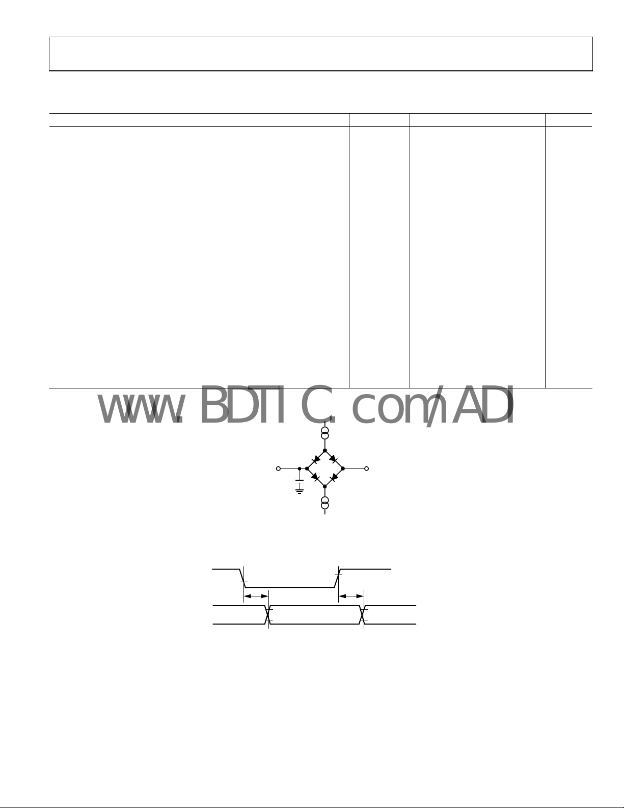
ANALOG INPUTS
Input Structure
Figure 27 shows an equivalent circuit of the input structure of
the AD7949. The two diodes, D1 and D2, provide ESD
protection for the analog inputs, IN[7:0] and COM. Care must
be taken to ensure that the analog input signal does not exceed
the supply rails by more than 0.3 V because this causes the
diodes to become forward biased and to start conducting
current.
These diodes can handle a forward-biased current of 130 mA
max
imum. For instance, these conditions may eventually occur
when the input buffer supplies are different from VDD. In such
a case, for example, an input buffer with a short circuit, the
current limitation can be used to protect the part.
DD
INx+
OR INx–
OR COM
GND
Figure 27. Equivalent Analog Input Circuit
This analog input structure allows the sampling of the true
differential signal between INx+ and COM or INx+ and INx−.
(COM or INx− = GND ± 0.1 V or V
differential inputs, signals common to both inputs are rejected,
as shown in
Figure 28.
D1
C
PIN
D2
R
± 0.1 V). By using these
REF
C
IN
IN
07351-030
70
65
60
55
50
CMRR (dB)
45
40
35
30
1
Figure 28. Analog Input CMRR vs. Frequency
100
FREQUENCY (kHz)
1k
10k10
07351-031
During the acquisition phase, the impedance of the analog
inputs can be modeled as a parallel combination of the
capacitor, C
connection of R
R
is typically 3.5 kΩ and is a lumped component made up of
IN
serial resistors and the on resistance of the switches. C
, and the network formed by the series
PIN
and CIN. C
IN
is primarily the pin capacitance.
PIN
is
IN
typically 27 pF and is mainly the ADC sampling capacitor.
Selectable Low Pass Filter
During the conversion phase, where the switches are opened,
the input impedance is limited to C
acquiring, R
and CIN make a one-pole, low-pass filter that
IN
. While the AD7949 is
PIN
reduces undesirable aliasing effects and limits the noise from
the driving circuitry. The low pass filter can be programmed for
the full bandwidth or ¼ of the bandwidth with CFG[6] as shown in
Tabl e 9. Note that the converters throughout must also be
educed by ¼ when using the filter. If the maximum throughput
r
is used with the BW set to ¼, the converter acquisition time,
t
, will be violated, resulting in increased THD.
ACQ
Input Configurations
Figure 29 shows the different methods for configuring the analog
inputs with the configuration register (CFG[12:10]). Refer to
the Configuration Register, CFG, section for more details.
Rev. A | Page 17 of 28

AD7949
www.BDTIC.com/ADI
CH0+
CH1+
CH2+
CH3+
CH4+
CH5+
CH6+
CH7+
CH0+ (–)
CH0– (+)
CH1+ (–)
CH1– (+)
CH2+ (–)
CH2– (+)
CH3+ (–)
CH3– (+)
A—8 CHANNELS,
SINGLE ENDED
C—4 CHANNELS,
IN0
IN1
IN2
IN3
IN4
IN5
IN6
IN7
COM
GND
IN0
IN1
IN2
IN3
IN4
IN5
IN6
IN7
COM
GND
DIFFERENTI AL
Figure 29. Multiplexed Analog Input Configuraitons
The analog inputs can be configured as
• Figure 29A, single ended referenced to system ground;
11
CFG[12:10] = 1
.
2
• Figure 29B, bipolar differential with a common reference
po
int; COM = V
/2; CFG[12:10] = 0102.
REF
Unipolar differential with COM connected to a ground
sense; CFG[12:10] = 110
• Figure 29C, bipolar differential pairs with INx− referenced
to
V
/2; CFG[12:10] = 00X2.
REF
Unipolar differential pairs with INx− referenced to a
ground sense; CFG[12:10] = 10X
In this configuration, the INx+ is identified by the channel
in CFG[9:7]. Example: for IN0 = IN1+ and IN1 = IN1−,
CFG[9:7] = 000
CFG[9:7] = 001
; for IN1 = IN1+ and IN0 = IN1−,
2
.
2
• Figure 29D, inputs configured in any of the above combin-
a
tions (showing that the AD7949 can be configured
dynamically).
Sequencer
The AD7949 includes a channel sequencer useful for scanning
channels in a IN0 to INx fashion. Channels are scanned as
singles or pairs, with or without the temperature sensor, after
the last channel is sequenced.
.
2
CH0+
CH1+
CH2+
CH3+
CH4+
CH5+
CH6+
CH7+
COM–
B—8 CHANNELS,
COMMON REFERNCE
CH0+ (–)
CH0– (+)
CH1+ (–)
CH1– (+)
CH2+
CH3+
CH4+
CH5+
COM–
D—COMBINATI ON
.
2
IN0
IN1
IN2
IN3
IN4
IN5
IN6
IN7
COM
GND
IN0
IN1
IN2
IN3
IN4
IN5
IN6
IN7
COM
GND
07351-032
The sequencer starts with IN0 and finishes with INx set in
CFG[9:7]. F
or paired channels, the channels are paired
depending on the last channel set in CFG[9:7]. Note that the
channel pairs are always paired IN (even) = INx+ and IN (odd)
= INx− regardless of CFG[7].
To enable the sequencer, CFG[2:1] are written to for initializing
th
e sequencer. After CFG[13:0] is updated, DIN must be held
low while reading data out (at least for Bit 13), or the CFG will
begin updating again.
While operating in a sequence, the CFG can be changed by
wr
iting 01
to CFG[2:1]. However, if changing CFG11 (paired
2
or single channel) or CFG[9:7] (last channel in sequence), the
sequence reinitializes and converts IN0 (or IN1) after CFG is
updated.
Examples
Only the bits for input and sequencer are highlighted.
As a first example, scan all IN[7:0] referenced to COM = GND
th temperature sensor.
wi
13 12 11 10 9 8 7 6 5 4 3 2 1 0
CFG INCC INx BW REF SEQ RB
- 1 1 0 1 1 1 - - - - 1 0 -
As a second example, scan three paired channels without
temperature sensor and referenced to V
13 12 11 10 9 8 7 6 5 4 3 2 1 0
CFG INCC INx BW REF SEQ RB
- 0 0 X 1 0 X - - - - 1 1 -
REF
/2.
Source Resistance
When the source impedance of the driving circuit is low, the
AD7949 can be driven directly. Large source impedances
significantly affect the ac performance, especially total harmonic
distortion (THD). The dc performances are less sensitive to the
input impedance. The maximum source impedance depends on
the amount of THD that can be tolerated.
DRIVER AMPLIFIER CHOICE
Although the AD7949 is easy to drive, the driver amplifier must
meet the following requirements:
• The
• Fo
noise generated by the driver amplifier must be kept as
low as possible to preserve the SNR and transition noise
performance of the AD7949. Note that the AD7949 has a
noise much lower than most of the other 14-bit ADCs and,
therefore, can be driven by a noisier amplifier to meet a
given system noise specification. The noise from the
amplifier is filtered by the AD7949 analog input circuit
low-pass filter made by R
and CIN or by an external filter,
IN
if one is used.
r ac applications, the driver should have a THD
performance commensurate with the AD7949. Figure 17
s
hows THD vs. frequency for the AD7949.
Rev. A | Page 18 of 28

AD7949
www.BDTIC.com/ADI
• For multichannel, multiplexed applications on each input
or input pair, the driver amplifier and the AD7949 analog
input circuit must settle a full-scale step onto the capacitor
array at a 14-bit level (0.0015%). In the amplifier data
sheet, settling at 0.1% to 0.01% is more commonly
specified. This may differ significantly from the settling
time at a 14-bit level and should be verified prior to driver
selection.
Table 8. Recommended Driver Amplifiers
Amplifier Typical Application
ADA4841-x Very low noise, small, and low power
AD8655 5 V single supply, low noise
AD8021 Very low noise and high frequency
AD8022 Low noise and high frequency
OP184 Low power, low noise, and low frequency
AD8605, AD8615 5 V single supply, low power
VOLTAGE REFERENCE OUTPUT/INPUT
The AD7949 allows the choice of a very low temperature drift
internal voltage reference, an external reference, or an external
buffered reference.
The internal reference of the AD7949 provides excellent perfor-
nce and can be used in almost all applications. There are six
ma
possible choices of voltage reference schemes briefly described
in
Tabl e 9 with more details in each of the following sections.
Internal Reference/Temperature Sensor
The internal reference can be set for either 2.5 V or a 4.096 V
output as detailed in Tab le 9 . With the internal reference
bled, the band gap voltage is also present on the REFIN pin,
ena
which requires an external 0.1 F capacitor. Because the current
output of REFIN is limited, it can be used as a source if followed
by a suitable buffer, such as the
Enabling the reference also enables the internal temperature
ensor, which measures the internal temperature of the AD7949
s
and is thus useful for performing a system calibration. Note
that, when using the temperature sensor, the output is straight
binary referenced from the AD7949 GND pin.
The internal reference is temperature-compensated to within
. The reference is trimmed to provide a typical drift of
15 mV
3 ppm/°C.
AD8605.
External Reference and Internal Buffer
For improved drift performance, an external reference can be
used with the internal buffer. The external reference is connected to REFIN, and the output is produced on the REF pin.
An external reference can be used with the internal buffer with
or without the temperature sensor enabled. Refer to
th
e register details. With the buffer enabled, the gain is unity and is
limited to an input/output of 4.096 V.
Tabl e 9 for
The internal reference buffer is useful in multiconverter appli-
tions because a buffer is typically required in these applications.
ca
In addition, a low power reference can be used because the
internal buffer provides the necessary performance to drive the
SAR architecture of the AD7949.
External Reference
In any of the six voltage reference schemes, an external reference
can be connected directly on the REF pin because the output
impedance of REF is >5 k. To reduce power consumption, the
reference and buffer can be powered down independently or
together for the lowest power consumption. However, for
applications requiring the use of the temperature sensor, the
reference must be active. Refer to
For improved drift performance, an external reference such as
th
e ADR43x or ADR44x is recommended.
Tabl e 9 for register details.
Reference Decoupling
Whether using an internal or external reference, the AD7949
voltage reference output/input, REF, has a dynamic input
impedance and should therefore be driven by a low impedance
source with efficient decoupling between the REF and GND pins.
This decoupling depends on the choice of the voltage reference
but usually consists of a low ESR capacitor connected to REF
and GND with minimum parasitic inductance. A 10 µF (X5R,
1206 size) ceramic chip capacitor is appropriate when using the
internal reference, the
w impedance buffer such as the AD8031 or the AD8605.
a lo
The placement of the reference decoupling capacitor is also
i
mportant to the performance of the AD7949, as explained in the
Layout section. The decoupling capacitor should be mounted on
e same side as the ADC at the REF pin with a thick PCB trace.
th
The GND should also connect to the reference decoupling
capacitor with the shortest distance and to the analog ground
plane with several vias.
If desired, smaller reference decoupling capacitor values down
o 2.2 µF can be used with a minimal impact on performance,
t
especially on DNL.
Regardless, there is no need for an additional lower value
mic decoupling capacitor (for example, 100 nF) between the
cera
REF and GND pins.
For applications that use multiple AD7949s or other PulSAR
de
vices, it is more effective to use the internal reference buffer
to buffer the external reference voltage, thus reducing SAR
conversion crosstalk.
The voltage reference temperature coefficient (TC) directly impacts
f
ull scale; therefore, in applications where full-scale accuracy
matters, care must be taken with the TC. For instance, a
±61 ppm/°C TC of the reference changes full scale by ±1 LSB/°C.
ADR43x /ADR44x external reference, or
Rev. A | Page 19 of 28

AD7949
www.BDTIC.com/ADI
POWER SUPPLY
The AD7949 uses three power supply pins: two core supplies
(VDD) and a digital input/output interface supply (VIO). VIO
allows direct interface with any logic between 1.8 V and VDD.
To reduce the supplies needed, the VIO and VDD pins can be
tied together. The AD7949 is independent of power supply
sequencing between VIO and VDD. The only restriction is that
CNV must be low during power up. Additionally, it is very
insensitive to power supply variations over a wide frequency
range, as shown in
75
70
65
60
55
50
PSSR (dB)
45
40
35
30
1
The AD7949 powers down automatically at the end of each
conversion phase; therefore, the operating currents and power
scale linearly with the sampling rate. This makes the part ideal
for low sampling rates (even of a few hertz) and low batterypowered applications.
Figure 30.
100
FREQUENCY (kHz)
Figure 30. PSRR vs. Frequency
1k
10k10
07351-034
10000
VDD = 5V, INTE RNAL REF
1000
100
10
0.1
OPERATING CURRENT (µA)
0.010
0.001
VDD = 5V, EXTE RNAL REF
1
10
VDD = 2.5V, EXT ERNAL REF
1k 10k
SAMPLING RAT E (sps)
VIO
100k
1M100
07351-040
Figure 31. Operating Currents vs. Sampling Rate
SUPPLYING THE ADC FROM THE REFERENCE
For simplified applications, the AD7949, with its low operating
current, can be supplied directly using the reference circuit as
shown in Figure 32. The reference line can be driven by
• The
• A r
• A r
system power supply directly
eference voltage with enough current output capability,
such as the ADR43x/ADR44x
eference buffer, such as the AD8605, which can also
ilter the system power supply, as shown in Figure 32
f
5V
10kΩ
5V
1µF
AD8605
5V
10Ω
1µF
10µF
1
0.1µF
AD7949
0.1µF
VIOREF VDD
1
OPTIO NAL REFERENCE BUFFE R AND FILTER.
Figure 32. Example of an Application
Rev. A | Page 20 of 28
Circuit
7351-035

AD7949
www.BDTIC.com/ADI
DIGITAL INTERFACE
The AD7949 uses a simple 4-wire interface and is compatible
with SPI, MICROWIRE™, QSPI™, digital hosts, and DSPs, for
example, Blackfin® ADSP-BF53x, SHARC®, ADSP-219x, and
ADSP-218x.
The interface uses the CNV, DIN, SCK, and SDO signals and
a
llows CNV, which initiates the conversion, to be independent
of the readback timing. This is useful in low jitter sampling or
simultaneous sampling applications.
A 14-bit register, CFG[13:0], is used to configure the ADC for
t
he channel to be converted, the reference selection, and other
components, which are detailed in the Configuration Register,
CFG, section.
When CNV is low, reading/writing can occur during conversion,
acq
uisition, and spanning conversion (acquisition plus conversion),
as detailed in the following sections. The CFG word is updated
on the first 14 SCK rising edges, and conversion results are read
back on the first 13 (or 14 if busy mode is selected) SCK falling
edges. If the CFG readback is enabled, an additional
14 SCK falling edges are required to read back the CFG word
associated with the conversion results with the CFG MSB
following the LSB of the conversion result.
A discontinuous SCK is recommended because the part is
elected with CNV low and SCK activity begins to write a new
s
configuration word and clock out data.
Note that in the following sections, the timing diagrams
te digital activity (SCK, CNV, DIN, SDO) during the
indica
conversion. However, due to the possibility of performance
degradation, digital activity should occur only prior to the safe
data reading/writing time, t
error correction circuitry that can correct for an incorrect bit
during this time. From t
correction and conversion results may be corrupted. The user
should configure the AD7949 and initiate the busy indicator (if
desired) prior to t
by having SCK or DIN transitions near the sampling instant.
Therefore, it is recommended to keep the digital pins quiet for
approximately 30 ns before and 10 ns after the rising edge of
CNV, using a discontinuous SCK whenever possible to avoid
any potential performance degradation.
. It is also possible to corrupt the sample
DATA
, because the AD7949 provides
DATA
DATA
to t
, there is no error
CONV
Reading/Writing During Conversion, Fast Hosts
When reading/writing during conversion (n), conversion
results are for the previous (n − 1) conversion, and writing the
CFG is for the next (n + 1) acquisition and conversion.
After the CNV is brought high to initiate conversion, it must be
rought low again to allow reading/writing during conversion.
b
Reading/writing should only occur up to t
time is limited, the host must use a fast SCK.
The SCK frequency required is calculated by
EdgesSCKNumber
DATA
CONV
__
is a safe time when digital
f
≥
SCK
The time between t
activity should not occur, or sensitive bit decisions may be
corrupt.
DATA
t
and t
and, because this
DATA
Reading/Writing During Acquisition, Any Speed Hosts
When reading/writing during acquisition (n), conversion
results are for the previous (n − 1) conversion, and writing is for
the (n + 1) acquisition.
For the maximum throughput, the only time restriction is that
he reading/writing take place during the t
t
slow throughputs, the time restriction is dictated by throughput
required by the user, and the host is free to run at any speed.
Thus for slow hosts, data access must take place during the
acquisition phase.
(min) time. For
ACQ
Reading/Writing Spanning Conversion, Any Speed Host
When reading/writing spanning conversion, the data access
starts at the current acquisition (n) and spans into the
conversion (n). Conversion results are for the previous (n − 1)
conversion, and writing the CFG is for the next (n + 1) acquisition
and conversion.
Similar to reading/writing during conversion, reading/writing
ld only occur up to t
shou
the only time restriction is that reading/writing take place
during the t
For slow throughputs, the time restriction is dictated by the
er’s required throughput, and the host is free to run at any
us
speed. Similar to the reading/writing during acquisition, for
slow hosts, the data access must take place during the
acquisition phase with additional time into the conversion.
Note that data access spanning conversion requires the CNV to
e driven high to initiate a new conversion, and data access is
b
not allowed when CNV is high. Thus, the host must perform
two bursts of data access when using this method.
(min) + t
ACQ
. For the maximum throughput,
DATA
time.
DATA
Rev. A | Page 21 of 28

AD7949
www.BDTIC.com/ADI
CONFIGURATION REGISTER, CFG
The AD7949 uses a 14-bit configuration register (CFG[13:0]) as
detailed in Tab le 9 for configuring the inputs, channel to be
nverted, one-pole filter bandwidth, reference, and channel
co
sequencer. The CFG is latched (MSB first) on DIN with 14 SCK
rising edges. The CFG update is edge dependent, allowing for
asynchronous or synchronous hosts.
The register can be written to during conversion, during acquis-
tion, or spanning acquisition/conversion and is updated at the
i
end of conversion, tCONV (max). There is always a one deep delay
when writing CFG. Note that, at power up, the CFG is undefined,
13 12 11 10 9 8 7 6 5 4 3 2 1 0
CFG INCC INCC INCC INx INx INx BW REF REF REF SEQ SEQ RB
Table 9. Configuration Register Description
Bit(s) Name Description
<13> CFG Configuration update.
0 = Keep current configuration settings.
1 = Overwrite contents of register.
<12:10> INCC Input channel configuration. Selection of pseudobipolar, pseudodifferential, pairs, single-ended or temperature sensor. Refer to
0 0 X Bipolar differential pairs; INx− referenced to V
0 1 0 Bipolar; INx referenced to COM = V
0 1 1 Temperature sensor.
1 0 X Unipolar differential pairs; INx− referenced to GND ±0.1 mV.
1 1 0 Unipolar, IN0 to IN7 referenced to COM = GND ±0.1 V (GND sense).
<9:7> INx Input channel selection in binary fashion.
0 0 0 IN0
0 0 1 IN1
… … …
<6> BW
<5:3> REF
0 0 0 Internal reference, REF = 2.5 V output.
0 0 1 Internal reference, REF = 4.096 V output.
0 1 0 External reference, temperature enabled.
0 1 1 External reference, internal buffer, temperature enabled.
1 1 0 External reference, temperature disabled.
<2:1> SEQ
0 0 Disable sequencer.
0 1 Update configuration during sequence.
1 0 Scan IN0 to INx (set in CFG[9:7]), then temperature.
0 RB Read back the CFG register.
the
Input Configurations section.
Bit 12 Bit 11 Bit 10 Function
1 1 1 Unipolar, IN0 to IN7 referenced to GND.
Bit 9 Bit 8 Bit 7 Channel
1 1 1 IN7
Select bandwidth for low-pass filter. Refer to the
0 = ¼ of BW, uses an additional series resistor to further bandwidt
¼ also.
1 = Full BW.
Reference/buffer selection. Selection of internal, and external, exter
sensor. Refer to the
Bit 5 Bit 4 Bit 3 Function
1 1 1 External reference, internal buffer, temperature disabled.
Channel sequencer. Allows for scanning channels i
Bit 2 Bit 1 Function
1 1 Scan IN0 to INx (set in CFG[9:7]).
0 = Read back current configuration at end of data.
1 = Do not read back contents of configuration.
Voltage Reference Output/Input section.
Selectable Low Pass Filter section.
Rev. A | Page 22 of 28
and two dummy conversions are required to update the register.
o preload the CFG with a factory setting, hold DIN high for two
T
conversions. Thus CFG[13:0] = 0x3FFF. This sets the AD7949 for
• IN[7:0] uni
• F
ull bandwidth for one-pole filter
• I
nternal reference/temperature sensor disabled, buffer
polar referenced to GND, sequenced in order
enabled
readback of CFG
• No
Tabl e 9 summarizes the configuration register bit details. See
th
e Theory of Operation section for more details.
/2 ±0.1 V.
REF
/2 ±0.1 V.
REF
h limit the noise. Maximum throughout must be reduced to
nal buffered, and enabling of the on-chip temperature
n an IN0 to INx fashion. Refer to the Sequencer section.

AD7949
www.BDTIC.com/ADI
READ/WRITE SPANNING CONVERSION WITHOUT A BUSY INDICATOR
This mode is used when the AD7949 is connected to any host
using an SPI, serial port, or FPGA. The connection diagram is
shown in Figure 33, and the corresponding timing is given in
Figure 34. For SPI, the host should use CPHA = CPOL = 0.
Re
ading/writing spanning conversion is shown, which covers
all three modes detailed in the
A rising edge on CNV initiates a conversion, forces SDO to
h impedance, and ignores data present on DIN. After a
hig
conversion is initiated, it continues until completion
irrespective of the state of CNV. CNV must be returned high
before the safe data transfer time, t
beyond the conversion time, t
busy signal indicator.
After the conversion is complete, the AD7949 enters the
acq
uisition phase and powers down. When the host brings
CNV low after t
(max), the MSB is enabled on SDO. The
CONV
host also must enable the MSB of CFG at this time (if necessary)
Digital Interface section.
, and then held high
DATA
, to avoid generation of the
CONV
AD7949
CNV
SDO
DIN
SCK
to begin the CFG update. While CNV is low, both a CFG
update and a data readback take place. The first 14 SCK rising
edges are used to update the CFG, and the first 13 SCK falling
edges clock out the conversion results starting with MSB − 1.
The restriction for both configuring and reading is that they
both occur before the t
time of the next conversion elapses.
DATA
All 14 bits of CFG[13:0] must be written or they are ignored.
Also, if the 14-bit conversion result is not read back before t
DATA
elapses, it is lost.
The SDO data is valid on both SCK edges. Although the rising
edg
e can be used to capture the data, a digital host using the
SCK falling edge allows a faster reading rate, provided it has an
acceptable hold time. After the 14
th
(or 28th) SCK falling edge, or
when CNV goes high (whichever occurs first), SDO returns to
high impedance. If CFG readback is enabled, the CFG associated with the conversion result (n − 1) is read back MSB first
following the LSB of the conversion result. A total of 30 SCK
falling edges is required to return SDO to high impedance if
this is enabled.
DIGITAL HOST
SS
MISO
MOSI
SCK
ACQUISI TION
CNV
(n - 1)
SCK
DIN
SDO
t
DATA
CONVERSION (n – 1)
t
EN
t
END DATA (n – 2)
DIS
>
t
CONV
t
CONV
13
12
X
X
END CFG (n)
LSB + 1
FOR SPI US E CPHA = 0, CPOL = 0.
Figure 33. Connection Diagram for the AD7
t
CYC
RETURN CNV HIGH
FOR NO BUSY
(QUIET
TIME)
UPDATE (n)
14/
28
CFG
LSB
LSB
NOTES:
1. THE LSB I S FOR CONVERS ION RESULTS O R THE CONFI GURATIO N REGIST ER CFG (n – 1) IF
15 SCK FALLI NG EDGES = LSB OF CO NVERSION RESULT S.
29 SCK FALLI NG EDGES = LSB OF CO NFIGURATI ON REGI STER.
ON THE 16TH OR 30TH SCK FAL LING EDG E, SDO I S DRIVEN TO HI GH IMPE NDANCE.
CFG/SDO
t
CLSCK
t
EN
t
DIS
t
ACQ
ACQUISI TION ( n)
1
2
t
SDINtHDIN
CFG
CFG
MSB – 1
MSB
BEGIN CFG (n + 1)
MSB
MSB – 1
BEGIN DATA ( n – 1)
949 Without a Busy Indicator
t
HSDO
t
DSDO
t
t
07351-036
CNVH
EN
t
DIS
Figure 34. Serial Interface Timing for the AD7949 Without a Busy Indicator
t
DATA
CONVERSIO N (n)
13
12
X
END CFG (n + 1)
LSB + 1
END DATA (n – 1)
t
CONV
SEE NOTE
X
CFG
LSB
14/
28
SEE NOTE
LSB
RETURN CNV HIGH
FOR NO BUSY
(QUIET
ACQUISITION
(n + 1)
UPDATE (n + 1 )
CFG/SDO
t
DIS
TIME)
07351-037
Rev. A | Page 23 of 28

AD7949
V
www.BDTIC.com/ADI
READ/WRITE SPANNING CONVERSION WITH A BUSY INDICATOR
This mode is used when the AD7949 is connected to any host
using an SPI, serial port, or FPGA with an interrupt input. The
connection diagram is shown in Figure 35, and the correspond
ing timing is given in Figure 36. For SPI, the host should use
A = CPOL = 1. Reading/writing spanning conversion is
CPH
shown, which covers all three modes detailed in the
erface section.
Int
A rising edge on CNV initiates a conversion, forces SDO to
hig
h impedance, and ignores data present on DIN. After a
conversion is initiated, it continues until completion
irrespective of the state of CNV. CNV must be returned low
before the safe data transfer time, t
beyond the conversion time, t
CONV
, and then held low
DATA
, to generate the busy signal
indicator. When the conversion is complete, SDO transitions
from high impedance to low with a pull-up to VIO, which can
be used to interrupt the host to begin data transfer.
After the conversion is complete, the AD7949 enters the
uisition phase and powers down. The host must enable the
acq
Digital
AD7949
SDO
CNV
DIN
SCK
MSB of CFG at this time (if necessary) to begin the CFG
update. While CNV is low, both a CFG update and a data
readback take place. The first 14 SCK rising edges are used to
update the CFG, and the first 14 SCK falling edges clock out the
conversion results starting with the MSB. The restriction for
both configuring and reading is that they both occur before the
t
time elapses for the next conversion. All 14 bits of
DATA
CFG[13:0] must be written or they are ignored. Also, if the 14-bit
conversion result is not read back before t
elapses, it is lost.
DATA
The SDO data is valid on both SCK edges. Although the rising
e can be used to capture the data, a digital host using the
edg
SCK falling edge allows a faster reading rate, provided it has an
acceptable hold time. After the optional 14
th
(or 28th) SCK
falling edge or when CNV goes high (whichever occurs first),
SDO returns to high impedance. If CFG readback is enabled,
the CFG associated with the conversion result (n − 1) is read
back MSB first following the LSB of the conversion result.
A total of 29 SCK falling edges is required to return SDO to
high impedance if this is enabled.
IO
DIGITAL HOST
MISO
IRQ
SS
MOSI
SCK
CNV
CONVERSION
(n – 1)
SCK
DIN
SDO
t
DATA
CONVERSION (n – 1)
14
13
END CFG (n)
LSB
+ 1
END DATA (n – 2)
FOR SPI US E CPHA = 1, CPOL = 1.
Figure 35. Connection Diagram for the AD7949 with a Busy Indicator
t
CYC
(QUIET
TIME)
UPDATE (n)
15/
29
LSB
CFG/SDO
CFG
MSB
t
DIS
t
EN
NOTES:
1. THE LSB I S FOR CONV ERSION RESUL TS OR THE CO NFIGURAT ION REG ISTER CFG (n – 1) IF
16 SCK FALLING EDGES = LSB OF CONVER SION RESUL TS.
30 SCK FALLING EDGES = LSB OF CO NFIGURATI ON REGISTER.
ON THE 17TH O R 31st SC K FALLING EDGE, SDO IS DRI VEN TO HIG H IMP ENDANCE.
OTHERWI SE, THE LSB REM AINS ACTI VE UNTIL THE BUSY INDICATO R IS DRI VEN LOW.
BEIGN CFG (n + 1)
MSB
t
ACQ
ACQUISI TIO N (n)
1
2
t
HDIN
t
SDIN
CFG
MSB –1
MSB
– 1
BEGIN DATA ( n – 1)
t
HSDO
t
DSDO
t
t
CNVH
EN
Figure 36. Serial Interface Timing for the AD7949 with a Busy Indicator
07351-038
t
DIS
t
CONV
t
DATA
CONVERSIO N (n)
SEE NOTE
14
13
XXXX
X
END CFG (n + 1)
LSB
END DATA (n – 1)
+ 1
15/
29
X
LSB
SEE NOTE
(QUIET
TIME)
t
DIS
ACQUISITION
UPDATE (n + 1 )
CFG/SDO
t
EN
(n + 1)
07351-039
Rev. A | Page 24 of 28

AD7949
www.BDTIC.com/ADI
APPLICATION HINTS
LAYOUT
The printed circuit board that houses the AD7949 should be
designed so that the analog and digital sections are separated
and confined to certain areas of the board. The pinout of the
AD7949, with all its analog signals on the left side and all its
digital signals on the right side, eases this task.
Avoid running digital lines under the device because these
uple noise onto the die unless a ground plane under the
co
AD7949 is used as a shield. Fast switching signals, such as CNV
or clocks, should not run near analog signal paths. Crossover of
digital and analog signals should be avoided.
At least one ground plane should be used. It can be common or
plit between the digital and analog sections. In the latter case,
s
the planes should be joined underneath the AD7949s.
The AD7949 voltage reference input REF has a dynamic input
pedance and should be decoupled with minimal parasitic
im
inductances. This is done by placing the reference decoupling
ceramic capacitor close to, ideally right up against, the REF and
GND pins and connecting them with wide, low impedance traces.
Finally, the power supplies VDD and VIO of the AD7949
hould be decoupled with ceramic capacitors, typically 100 nF,
s
placed close to the AD7949 and connected using short, wide
traces to provide low impedance paths and reduce the effect of
glitches on the power supply lines.
EVALUATING AD7949 PERFORMANCE
Other recommended layouts for the AD7949 are outlined in the
documentation of the evaluation board for the AD7949 (EVAL-
AD7949CBZ)
assembled and tested evaluation board, documentation, and
software for controlling the board from a PC via the evaluation
controller board,
. The evaluation board package includes a fully
EVAL-CONTROL BRD3.
Rev. A | Page 25 of 28

AD7949
C
www.BDTIC.com/ADI
OUTLINE DIMENSIONS
PIN 1
INDI
ATO R
1.00
0.85
0.80
SEATING
PLANE
0.08
0.50
BSC
0.50
0.40
0.30
0.60 MAX
15
11
16
EXPOSED
(BOTTOM VIEW)
10
12° MAX
4.00
BSC SQ
TOP VIEW
0.80 MAX
0.65 TYP
0.30
0.23
0.18
COMPLIANT
0.60 MAX
3.75
BSC SQ
0.05 MAX
0.02 NOM
COPLANARIT Y
0.20 REF
TO
JEDEC STANDARDS MO -220-VGGD-1
Figure 37. 20-Lead Lead Frame Chip Scale Package (LFCSP_VQ)
4 mm × 4 mm Body, Very Thin Quad
(CP-20-4)
Dim
ensions shown in millimeters
PAD
P
N
I
1
R
O
T
A
N
I
D
C
2.65
2.50 SQ
2.35
0.25 MIN
I
012508-B
20
1
5
6
ORDERING GUIDE
Temperature
Model
AD7949BCPZ
AD7949BCPZRL7
EVAL-AD7949CBZ
1
1
1
EVAL-CONTROL BRD3
1
Z = RoHS Compliant Part.
2
This controller board allows a PC to control and communicate with all Analog Devices evaluation boards whose model numbers end in CB.
R
ange Package Description
–40°C to +85°C 20-Lead QFN (LFCSP_VQ) CP-20-4 Tray, 490
–40°C to +85°C 20-Lead QFN (LFCSP_VQ) CP-20-4 Reel, 1,500
Evaluation Board
2
Controller Board
Package
Option
Ordering
Quantity
Rev. A | Page 26 of 28

AD7949
www.BDTIC.com/ADI
NOTES
Rev. A | Page 27 of 28

AD7949
www.BDTIC.com/ADI
NOTES
©2008 Analog Devices, Inc. All rights reserved. Trademarks and
registered trademarks are the property of their respective owners.
D07351-0-5/08(A)
Rev. A | Page 28 of 28
 Loading...