

LC2MOS 8-Channel, 12-Bit
A
V
www.BDTIC.com/ADI
FEATURES
Fast 12-bit ADC with 5.9 μs conversion time
Eight single-ended analog input channels
Selection of input ranges:
±10 V for AD7890-10
0 V to 4.096 V for AD7890-4
0 V to 2.5 V for AD7890-2
Allows separate access to multiplexer and ADC
On-chip track/hold amplifier
On-chip reference
High-speed, flexible, serial interface
Single supply, low-power operation (50 mW maximum)
Power-down mode (75 μW typ)
GENERAL DESCRIPTION
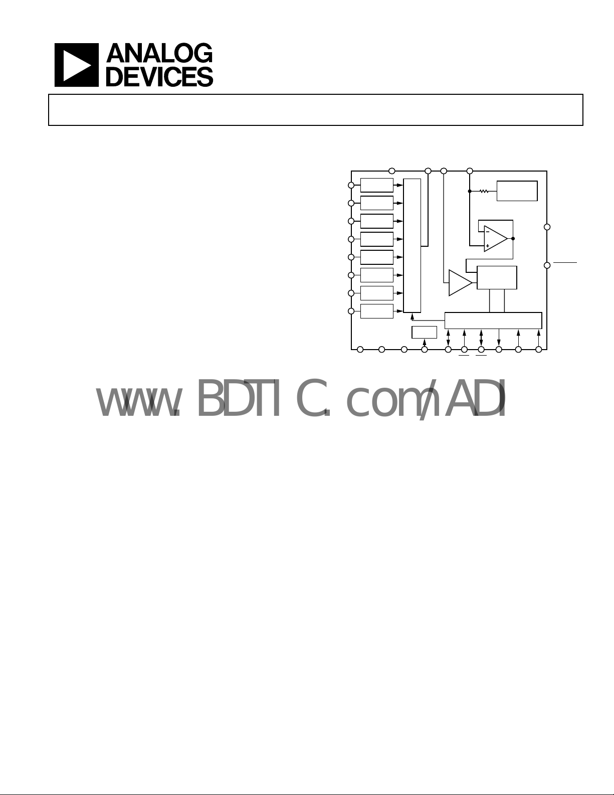
The AD7890 is an 8-channel 12-bit data acquisition system. The
part contains an input multiplexer, an on-chip track/hold
amplifier, a high speed 12-bit ADC, a 2.5 V reference, and a
high speed, serial interface. The part operates from a single 5 V
supply and accepts an analog input range of ±10 V (AD7890-10),
0 V to 4.096 V (AD7890-4), and 0 V to 2.5 V (AD7890-2).
Serial Data Acquisition System
AD7890
FUNCTIONAL BLOCK DIAGRAM
MUX
SH
DD
V
V
V
V
V
V
V
V
SIGNAL
IN1
IN2
IN3
IN4
IN5
IN6
IN7
IN8
AGND AGND DGND SCLK TFS RFS DATA
SCALING
SIGNAL
SCALING
SIGNAL
SCALING
SIGNAL
SCALING
SIGNAL
SCALING
SIGNAL
SCALING
SIGNAL
SCALING
SIGNAL
SCALING
AD7890
1
1
1
1
1
1
1
1
MUX
CLOCK
OUT
TRACK/HOL D
CLK
IN
REF OUT/
IN
REF IN
2kΩ
OUTPUT/CONTROL REGISTER
1
NO SCALING ON AD7890-2
Figure 1.
REFERENCE
12-BIT
ADC
OUT
2.5V
DATAINSMODE
C
EXT
CONVST
01357-001
The multiplexer on the part is independently accessible. This
al
lows the user to insert an antialiasing filter or signal
conditioning, if required, between the multiplexer and the
ADC. This means that one antialiasing filter can be used for all
eight channels. Connection of an external capacitor allows the
user to adjust the time given to the multiplexer settling to
include any external delays in the filter or signal conditioning
circuitry.
Output data from the AD7890 is provided via a high speed
b
idirectional serial interface port. The part contains an on-chip
control register, allowing control of channel selection,
conversion start, and power-down via the serial port. Versatile,
high speed logic ensures easy interfacing to serial ports on
microcontrollers and digital signal processors.
In addition to the traditional dc accuracy specifications such as
linea
rity, full-scale, and offset errors, the AD7890 is also
specified for dynamic performance parameters including
harmonic distortion and signal-to-noise ratio.
Power dissipation in normal mode is low at 30 mW typical and the
part can be placed in a standby (power-down) mode if it is not
required to perform conversions. The AD7890 is fabricated in
Analog Devices, Inc.’s Linear Compatible CMOS (LC
2
MOS)
process, a mixed technology process that combines precision
bipolar circuits with low power CMOS logic. The part is available
in a 24-lead, 0.3" wide, plastic or ceramic dual-in-line package or in
a 24-lead small outline package (SOIC_W).
PRODUCT HIGHLIGHTS
1. Complete 12-Bit Data Acquisition System-on-a-Chip.
The AD7890 is a complete monolithic ADC combining an
8-channel multiplexer, 12-bit ADC, 2.5 V reference, and a
track/hold amplifier on a single chip.
eparate Access to Multiplexer and ADC.
2. S
The AD7890 provides access to the output of the
multiplexer allowing one antialiasing filter for 8 channels—
a considerable savings over the 8 antialiasing filters required if
the multiplexer is internally connected to the ADC.
gh Speed Serial Interface.
3. Hi
The part provides a high speed serial interface for easy
connection to serial ports of microcontrollers and DSP
processors.
Rev. C
Information furnished by Analog Devices is believed to be accurate and reliable. However, no
responsibility is assumed by Anal og Devices for its use, nor for any infringements of patents or ot her
rights of third parties that may result from its use. Specifications subject to change without notice. No
license is granted by implication or otherwise under any patent or patent rights of Analog Devices.
Trademarks and registered trademarks are the property of their respective owners.
One Technology Way, P.O. Box 9106, Norwood, MA 02062-9106, U.S.A.
Tel: 781.329.4700 www.analog.com
Fax: 781.461.3113 ©2006 Analog Devices, Inc. All rights reserved.

AD7890
www.BDTIC.com/ADI
TABLE OF CONTENTS
Features.............................................................................................. 1
Serial Interface ................................................................................ 17
General Description ......................................................................... 1
Functional Block Diagram .............................................................. 1
Product Highlights ........................................................................... 1
Revision History ............................................................................... 2
Specifications..................................................................................... 3
Timing Specifications .................................................................. 5
Absolute Maximum Ratings............................................................ 6
ESD Caution.................................................................................. 6
Pin Configuration and Function Descriptions............................. 7
Terminology ...................................................................................... 9
Control Register.............................................................................. 10
Theory of Operation ...................................................................... 11
Converter Details........................................................................ 11
Circuit Description..................................................................... 11
Track/Hold Amplifier ................................................................ 12
Self-Clocking Mode ................................................................... 17
External Clocking Mode ........................................................... 18
Simplifying the Interface........................................................... 19
Microprocessor/Microcontroller Interface................................. 20
AD7890 to 8051 Interface ......................................................... 20
AD7890 to 68HC11 Interface................................................... 20
AD7890 to ADSP-2101 Interface ............................................. 21
AD7890 to DSP56000 Interface ............................................... 21
AD7890 to TMS320C25/30 Interface...................................... 21
Antialiasing Filter....................................................................... 22
Performance.................................................................................... 23
Linearity....................................................................................... 23
Noise ............................................................................................ 23
Dynamic Performance............................................................... 24
Effective Number of Bits ........................................................... 24
Reference ..................................................................................... 13
Timing and Control ................................................................... 13
C
Functioning......................................................................... 16
EXT
REVISION HISTORY
9/06—Rev. B to Rev. C
Updated Format..................................................................Universal
Changes to Table 1............................................................................ 3
Updated Outline Dimensions....................................................... 25
Changes to Ordering Guide.......................................................... 27
2/01—Rev. A to Rev. B
Outline Dimensions....................................................................... 25
Ordering Guide .......................................................................... 27
Rev. C | Page 2 of 28

AD7890
www.BDTIC.com/ADI
SPECIFICATIONS
VDD = 5 V, AGND = DGND = 0 V, REF IN = 2.5 V, f
T
, unless otherwise noted.
MAX
Table 1.
Parameter A Versions1B Versions S Version Unit Test Conditions/Comments
DYNAMIC PERFORMANCE
Signal to (Noise + Distortion) Ratio270 70 70 dB min fIN = 10 kHz sine wave, f
Total Harmonic Distortion (THD)2
Peak Harmonic or Spurious Noise2
Intermodulation Distortion
2nd Order Terms −80 −80 −80 dB typ
3rd Order Terms −80 −80 −80 dB typ
Channel-to-Channel Isolation2
DC ACCURACY
Resolution 12 12 12 Bits
Min. Resolution for Which No
Missing Codes Are Guaranteed
Relative Accuracy2
Differential Nonlinearity2
Positive Full-Scale Error2
Full-Scale Error Match
AD7890-2, AD7890-4
Unipolar Offset Error2
Unipolar Offset Error Match 2 2 2 LSB max
AD7890-10 Only
Negative Full-Scale Error2
Bipolar Zero Error2
Bipolar Zero Error Match 2 2 2 LSB max
ANALOG INPUTS
AD7890-10
Input Voltage Range ±10 ±10 ±10 Volts
Input Resistance 20 20 20 kΩ min
AD7890-4
Input Voltage Range 0 to 4.096 0 to 4.096 0 to 4.096 Volts
Input Resistance 11 11 11 kΩ min
AD7890-2
Input Voltage Range 0 to 2.5 0 to 2.5 0 to 2.5 Volts
Input Current 50 50 200 nA max
MUX OUT OUTPUT
Output Voltage Range 0 to 2.5 0 to 2.5 0 to 2.5 Volts
Output Resistance
AD7890-10, AD7890-4 3/5 3/5 3/5 kΩ min/kΩ max
AD7890-2 2 2 2 kΩ max Assuming VIN is driven from low impedance
SHA IN INPUT
Input Voltage Range 0 to 2.5 0 to 2.5 0 to 2.5 Volts
Input Current ±50 ±50 ±50 nA max
REFERENCE OUTPUT/INPUT
REF IN Input Voltage Range 2.375/2.625 2.375/2.625 2.375/2.625 V min/V max 2.5 V ± 5%
Input Impedance 1.6 1.6 1.6 kΩ min Resistor connected to internal reference node
Input Capacitance
REF OUT Output Voltage 2.5 2.5 2.5 V nom
REF OUT Error @ 25°C ±10 ±10 ±10 mV max
T
to T
MIN
MAX
REF OUT Temperature Coefficient 25 25 25 ppm/°C typ
REF OUT Output Impedance 2 2 2 kΩ nom
4
5
±20 ±20 ±25 mV max
−77 −77 −77 dB max
−78 −78 −78 dB max
−80 −80 −80 dB max f
12 12 12 Bits
±1 ±0.5 ±1 LSB max
±1 ±1 ±1 LSB max
±2.5 ±2.5 ±2.5 LSB max
2 2 2 LSB max
±2 ±2 ±2 LSB max
±2 ±2 ±2 LSB max
±5 ±5 ±5 LSB max
10 10 10 pF max
= 2.5 MHz external, MUX OUT connect to SHA IN. All specifications T
CLK IN
CONVST
Rev. C | Page 3 of 28
Using external
fIN = 10 kHz sine wave, f
fIN = 10 kHz sine wave, f
fa = 9 kHz, fb = 9.5 kHz, f
= 1 kHz sine wave
IN
, any channel
= 100 kHz
SAMPLE
= 100 kHz3
SAMPLE
= 100 kHz3
SAMPLE
= 100 kHz3
SAMPLE
MIN
to
3

AD7890
www.BDTIC.com/ADI
Parameter A Versions1B Versions S Version Unit Test Conditions/Comments
LOGIC INPUTS
Input High Voltage, V
Input Low Voltage, V
Input Current, IIN ±10 ±10 ±10 μA max VIN = 0 V to VDD
Input Capacitance, C
LOGIC OUTPUTS
Output High Voltage, VOH 4.0 4.0 4.0 V min I
Output Low Voltage, VOL 0.4 0.4 0.4 V max I
Serial Data Output Coding
AD7890-10 Twos Complement
AD7890-4 Straight (Natural) Binary
AD7890-2 Straight (Natural) Binary
CONVERSION RATE
Conversion Time 5.9 5.9 5.9 μs max f
Track/Hold Acquisition Time2, 5
POWER REQUIREMENTS
VDD 5 5 5 V nom ± 5% for specified performance
IDD (Normal Mode) 10 10 10 mA max Logic inputs = 0 V or VDD
IDD (Standby Mode)6 @ 25°C 15 15 15 μA typ Logic inputs = 0 V or VDD
Power Dissipation
Normal Mode 50 50 50 mW max Typically 30 mW
Standby Mode @ 25°C 75 75 75 μW typ
1
Temperature ranges are as follows: A, B Versions: −40°C to +85°C; S Version: −55°C to +125°C.
2
See the Terminology section.
3
This sample rate is only achievable when using the part in external clocking mode.
4
Full-scale error match applies to positive full scale for the AD7890-2 and AD7890-4. It applies to both positive and negative full scale for the AD7890-10.
5
Sample tested @ 25°C to ensure compliance.
6
Analog inputs on AD7890-10 must be at 0 V to achieve correct power-down current.
2.4 2.4 2.4 V min VDD = 5 V ± 5%
INH
0.8 0.8 0.8 V max VDD = 5 V ± 5%
INL
5
IN
10 10 10 pF max
= 200 μA
SOURCE
= 1.6 mA
SINK
= 2.5 MHz, MUX OUT, connected to
CLK IN
SHA IN
2 2 2 μs max
Rev. C | Page 4 of 28

AD7890
www.BDTIC.com/ADI
TIMING SPECIFICATIONS
VDD = 5 V ± 5%, AGND = DGND = 0 V, REF IN = 2.5 V, f
Parameter1,
3
f
CLKIN
2.5 MHz max
t
CLKIN IN LO
t
CLK IN HI
4
tr
tf4
t
CONVERT
t
100 ns min
CST
Self-Clocking Mode
t1 t
5
t
25 ns max
2
t3 t
t4 t
5
t
5
t6 40 ns max
6
t
7
t8 0 ns min
t
t9 0 ns min
t10 20 ns min Data Valid to SCLK Falling Edge Setup Time.
t11 10 ns min Data Valid to SCLK Falling Edge Hold Time.
t12 20 ns min
External Clocking Mode
t13 20 ns min
5
t
14
t15 50 ns min SCLK High Pulse Width.
t16 50 ns min SCLK Low Pulse Width.
5
t
17
t18 20 ns min
6
t
19
6
t
19A
t20 20 ns min
t21 10 ns min Data Valid to SCLK Falling Edge Setup Time.
t22 15 ns min Data Valid to SCLK Falling Edge Hold Time.
t23 40 ns min
1
Sample tested at −25°C to ensure compliance. All input signals are specified with tr = tf = 5 ns (10% to 90% of 5 V) and timed from a voltage level of 1.6 V.
2
See Figure 10 to Figure 13.
3
The AD7890 is production tested with f
4
Specified using 10% and 90% points on waveform of interest.
5
These numbers are measured with the load circuit of Figure 2 and defined as the time required for the output to cross 0.8 V or 2.4 V.
6
These numbers are derived from the measured time taken by the data output to change 0.5 V when loaded with the circuit of Figure 2. The measured number is then
extrapolated back to remove effects of charging or discharging the 50 pF capacitor. This means that the times quoted in the timing characteristics are the true bus
relinquish times of the part and as such are independent of external bus loading capacitances.
2
Limit at T
, T
(A, B, S Versions) Unit Conditions/Comments
MIN
MAX
100 kHz min Master Clock Frequency. For specified performance.
0.3 × t
0 3 × t
ns min Master Clock Input Low Time.
CLK IN
ns min Master Clock Input High Time.
CLK IN
25 ns max Digital Output Rise Time. Typically 10 ns.
25 ns max Digital Output Fa
5.9 μs max Conversion Time.
+ 50 ns max
CLK IN HI
ns nom SCLK High Pulse Width.
CLK IN HI
ns nom SCLK Low Pulse Width.
CLK IN LO
20 ns max SCLK Rising Edge to Data Valid De
50 ns max Bus Relinquish Time after Rising Edge of SCLK.
+ 50 ns max
CLK IN
40 ns max
35 ns max SCLK Rising Edge to Data Valid De
50 ns max
90 ns max Bus Relinquish Time after Rising Edge of SCLK.
at 2.5 MHz. It is guaranteed by characterization to operate at 100 kHz.
CLK IN
= 2.5 MHz external, MUX OUT connected to SHA IN.
CLK IN
ll Time. Typically 10 ns.
CONVST
Pulse Width.
RFS
Low to SCLK Falling Edge.
RFS
Low to Data Valid Delay.
SCLK Rising Edge to
TFS
Low to SCLK Falling Edge.
Data Valid to
TFS
to SCLK Falling Edge Hold Time.
RFS
Low to SCLK Falling Edge Setup Time.
RFS
Low to Data Valid Delay.
RFS
to SCLK Falling Edge Hold Time.
RFS
Delay.
TFS
Falling Edge Setup Time (A2 Address Bit).
Bus Relinquish Time after Rising Edge of
TFS
Low to SCLK Falling Edge Setup Time.
TFS
to SCLK Falling Edge Hold Time.
lay.
lay.
RFS
.
1.6mA
TO OUTPUT
PIN
50pF
200µA
2.1V
01357-002
Figure 2. Load Circuit for Access Time and Bus Relinquish Time
Rev. C | Page 5 of 28
AD7890
www.BDTIC.com/ADI
ABSOLUTE MAXIMUM RATINGS
TA = 25°C, unless otherwise noted.
Parameter Rating
VDD to AGND −0.3 V to +7 V
VDD to DGND −0.3 V to +7 V
Analog Input Voltage to AGND
AD7890-10, AD7890-4 ±17 V
AD7890-2 −5 V, +10 V
Reference Input Voltage to AGND −0.3 V to VDD + 0.3 V
Digital Input Voltage to DGND −0.3 V to VDD + 0.3 V
Digital Output Voltage to DGND −0.3 V to VDD + 0.3 V
Operating Temperature Range
Commercial (A, B Versions) −40°C to +85°C
Extended (S Version) −55°C to +125°C
Storage Temperature Range −65°C to +150°C
Junction Temperature
PDIP Package, Power Dissipation 450 mW
θJA Thermal Impedance
Lead Temperature (Soldering, 10 sec)
CERDIP Package, Power Dissipation 450 mW
θJA Thermal Impedance 70°C/W
Lead Temperature (Soldering, 10 sec)
SOIC_W Package, Power Dissipation 450 mW
θJA Thermal Impedance 75°C/W
Lead Temperature, Soldering
Vapor Phase (60 sec)
Infrared (15 sec)
150°C
105°C/W
260°C
300°C
215°C
220°C
Stresses above those listed under Absolute Maximum Ratings
ma
rating only; functional operation of the device at these or any
other conditions above those indicated in the operational
section of this specification is not implied. Exposure to absolute
maximum rating conditions for extended periods may affect
device reliability.
ESD CAUTION
y cause permanent damage to the device. This is a stress
Rev. C | Page 6 of 28
AD7890
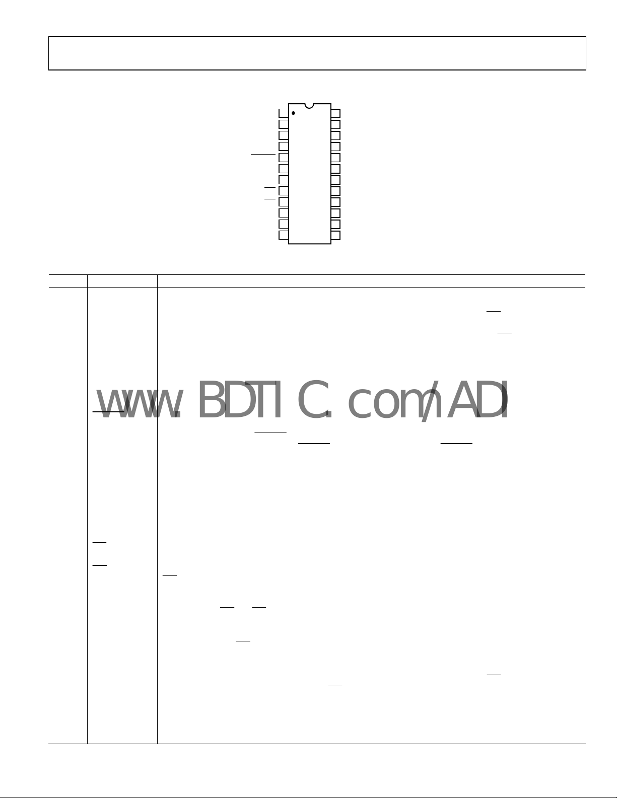
N
www.BDTIC.com/ADI
PIN CONFIGURATION AND FUNCTION DESCRIPTIONS
AGND
SMODE
DGND
C
EXT
CONVST
CLK IN
SCLK
TFS
RFS
DATA OUT
DATA IN
V
DD
1
2
3
4
AD7890
5
TOP VIEW
(Not to Scale)
6
7
8
9
10
11
12
24
REF OUT/RE F I
V
23
IN8
V
22
IN7
V
21
IN6
V
20
IN5
V
19
IN4
V
18
IN3
V
17
IN2
V
16
IN1
AGND
15
SHA IN
14
MUX OUT
13
01357-003
Figure 3. Pin Configuration
Table 2. Pin Function Descriptions
Pin No. Mnemonic Description
1 AGND Analog Ground. Ground reference for track/hold, comparator, and DAC.
2 SMODE
Control Input. Determines whether the part operates in its external clocking (slave) or self-clocking (master)
serial mode. With SMODE at a logic low, the part is in its self-clocking serial mode with RFS
outputs. This self-clocking mode is useful for connection to shift registers or to serial ports of DSP processors.
With SMODE at a logic high, the part is in its external clocking serial mode with SCLK and RFS
external clocking mode is useful for connection to the serial port of microcontrollers, such as the 8xC51 and
the 68HCxx, and for connection to the serial ports of DSP processors.
3 DGND
4 C
EXT
Digital Ground. Ground reference for digital circuitry.
External Capacitor. An external capacitor is connected to this pin to determine the length of the internal pulse
(see the Control Register section). Larger capacitances on this pin extend the pulse to allow for settling time
delays through an external antialiasing filter or signal conditioning circuitry.
5
CONVST
Convert Start. Edge-triggered logic input. A low-to-high transition on this input puts the track/hold into hold
and initiates conversion if the internal pulse has timed out (see the Control Register section). If the internal
pulse is active when the CONVST
goes high, the track/hold does not proceed to hold until the pulse times out.
If the internal pulse times out when CONVST goes high, the rising edge of CONVST drives the track/hold into
hold and initiates conversion.
6 CLK IN
Clock Input. An external TTL-compatible clock is applied to this input pin to provide the clock source for the
conversion sequence. In the self-clocking serial mode, the SCLK output is derived from this CLK IN pin.
7 SCLK
Serial Clock Input. In the external clocking (slave) mode (see the Serial Interface section), this is an externally
applied serial clock used to load serial data to the control register and to access data from the output register.
In the self-clocking (master) mode, the internal serial clock, which is derived from the clock input (CLK IN),
appears on this pin. Once again, it is used to load serial data to the control register and to access data from the
output register.
8
Transmit Frame Synchronization Pulse. Active low logic input with serial data expected after the falling edge of
TFS
this signal.
9
Receive Frame Synchronization Pulse. In the external clocking mode, this pin is an active low logic input with
RFS
RFS
provided externally as a strobe or framing pulse to access serial data from the output register. In the selfclocking mode, it is an active low output, which is internally generated and provides a strobe or framing pulse
for serial data from the output register. For applications which require that data be transmitted and received at
10 DATA OUT
the same time,
Serial Data Output. Sixteen bits of serial data are provided with one leading zero, preceding the three address
RFS and TFS should be connected together.
bits of the control register and the 12 bits of conversion data. Serial data is valid on the falling edge of SCLK for
sixteen edges after RFS
goes low. Output coding from the ADC is twos complement for the AD7890-10 and
straight binary for the AD7890-4 and AD7890-2.
11 DATA IN
Serial Data Input. Serial data to be loaded to the control register is provided at this input. The first five bits of
serial data are loaded to the control register on the first five falling edges of SCLK after TFS
12 V
Positive Supply Voltage, 5 V ± 5%.
DD
13 MUX OUT
on subsequent SCLK edges is ignored while TFS
Multiplexer Output. The output of the multiplexer appears a
remains low.
t this pin. The output voltage range from this
output is 0 V to 2.5 V for the nominal analog input range to the selected channel. The output impedance of this
output is nominally 3.5 kΩ. If no external antialiasing filter is required, MUX OUT should be connected to SHA IN.
and SCLK as
as inputs. This
goes low. Serial data
Rev. C | Page 7 of 28

AD7890
www.BDTIC.com/ADI
Pin No. Mnemonic Description
14 SHA IN
15 AGND Analog Ground. Ground reference for track/hold, comparator, and DAC.
16 V
17 V
18 V
19 V
20 V
21 V
22 V
23 V
24 REF OUT/REF IN
IN1
IN2
IN3
IN4
IN5
IN6
IN7
IN8
Track/Hold Input. The input to the on-chip track/hold is applied t
input voltage range is 0 V to 2.5 V.
Analog Input Channel 1. Single-ended analog input. The analog input range on is ±10 V (AD7890-10), 0 V to
V (AD7890-4), and 0 V to 2.5 V (AD7890-2). The channel to be converted is selected using the A0, A1, and
4.096
A2 bits in the control register. The multiplexer has guaranteed break-before-make operation.
Analog Input Channel 2. Single-ended analog input. The analog input range on is ±10 V (AD7890-10), 0 V to
V (AD7890-4), and 0 V to 2.5 V (AD7890-2). The channel to be converted is selected using the A0, A1, and
4.096
A2 bits in the control register. The multiplexer has guaranteed break-before-make operation.
Analog Input Channel 3. Single-ended analog input. The analog input range on is ±10 V (AD7890-10), 0 V to
V (AD7890-4), and 0 V to 2.5 V (AD7890-2). The channel to be converted is selected using the A0, A1, and
4.096
A2 bits in the control register. The multiplexer has guaranteed break-before-make operation.
Analog Input Channel 4. Single-ended analog input. The analog input range on is ±10 V (AD7890-10), 0 V to
V (AD7890-4), and 0 V to 2.5 V (AD7890-2). The channel to be converted is selected using the A0, A1, and
4.096
A2 bits in the control register. The multiplexer has guaranteed break-before-make operation.
Analog Input Channel 5. Single-ended analog input. The analog input range on is ±10 V (AD7890-10), 0 V to
V (AD7890-4), and 0 V to 2.5 V (AD7890-2). The channel to be converted is selected using the A0, A1, and
4.096
A2 bits in the control register. The multiplexer has guaranteed break-before-make operation.
Analog Input Channel 6. Single-ended analog input. The analog input range on is ±10 V (AD7890-10), 0 V to
V (AD7890-4), and 0 V to 2.5 V (AD7890-2). The channel to be converted is selected using the A0, A1, and
4.096
A2 bits in the control register. The multiplexer has guaranteed break-before-make operation.
Analog Input Channel 7. Single-ended analog input. The analog input range on is ±10 V (AD7890-10), 0 V to
V (AD7890-4), and 0 V to 2.5 V (AD7890-2). The channel to be converted is selected using the A0, A1, and
4.096
A2 bits in the control register. The multiplexer has guaranteed break-before-make operation.
Analog Input Channel 8. Single-ended analog input. The analog input range on is ±10 V (AD7890-10), 0 V to
V (AD7890-4) and 0 V to 2.5 V (AD7890-2). The channel to be converted is selected using the A0, A1, and
4.096
A2 bits in the control register. The multiplexer has guaranteed break-before-make operation.
Voltage Reference Output/Input. The part can be used with either its own internal reference or with an external
ference source. The on-chip 2.5 V reference voltage is provided at this pin. When using this internal reference
re
as the reference source for the part, REF OUT should decoupled to AGND with a 0.1 μF disc ceramic capacitor.
The output impedance of this reference source is typically 2 kΩ. When using an external reference source as
the reference voltage for the part, the reference source should be connected to this pin. This overdrives the
internal reference and provides the reference source for the part. The REF IN input is buffered on-chip. The
nominal reference voltage for correct operation of the AD7890 is 2.5 V.
o this pin. It is a high impedance input and the
Rev. C | Page 8 of 28

AD7890
www.BDTIC.com/ADI
TERMINOLOGY
Signal to (Noise + Distortion) Ratio
This is the measured ratio of signal to (noise + distortion) at the
utput of the A/D converter. The signal is the rms amplitude of
o
the fundamental. Noise is the rms sum of all nonfundamental
signals up to half the sampling frequency (f
/2), excluding dc.
S
The ratio is dependent upon the number of quantization levels
in the digitization process; the more levels, the smaller the
quantization noise. The theoretical signal to (noise + distortion)
ratio for an ideal N-bit converter with a sine wave input is given by:
Signal to (Noise + Distortion) = (6.02
N + 1.76) dB
Thus, for a 12-bit converter, this is 74 dB.
Total Harmonic Distortion
Total harmonic distortion (THD) is the ratio of the rms sum of
rmonics to the fundamental. For the AD7890, it is defined as
ha
2
2
2
2
THD
2
2
log20)dB(
=
4
3
V
1
VVVVV
++++
5
6
where:
is the rms amplitude of the fundamental and
V
1
V
, V3, V4, V5, and V6 are the rms amplitudes of the second
2
through the sixth harmonics.
Peak Harmonic or Spurious Noise
Peak harmonic or spurious noise is defined as the ratio of the
ms value of the next largest component in the ADC output
r
spectrum (up to f
/2 and excluding dc) to the rms value of the
S
fundamental. Normally, the value of this specification is
determined by the largest harmonic in the spectrum, but for
parts where the harmonics are buried in the noise floor, it is
determined by a noise peak.
Intermodulation Distortion
With inputs consisting of sine waves at two frequencies, fa and
fb
, any active device with nonlinearities creates distortion
products at sum and difference frequencies of mfa ± nfb where
m, n = 0, 1, 2, 3, and so on. Intermodulation terms are those for
which neither m nor n are equal to zero. For example, the
second-order terms include (fa + fb) and (fa − fb), while the
third-order terms include (2fa + fb), (2fa − fb), (fa + 2fb), and
(fa − 2fb).
The AD7890 is tested using the CCIF standard where two input
f
requencies near the top end of the input bandwidth are used.
In this case, the second and third order terms are of different
significance. The second-order terms are usually distanced in
frequency from the original sine waves while the third-order
terms are usually at a frequency close to the input frequencies.
As a result, the second- and third-order terms are specified
separately. The calculation of the intermodulation distortion is
as per the THD specification where it is the ratio of the rms
sum of the individual distortion products to the rms amplitude
of the fundamental expressed in dBs.
Rev. C | Page 9 of 28
Channel-to-Channel Isolation
Channel-to-channel isolation is a measure of the level of crosstalk
etween channels. It is measured by applying a full-scale 1 kHz
b
signal to any one of the other seven inputs and determining how
much that signal is attenuated in the channel of interest. The figure
given is the worst case across all eight channels.
Relative Accuracy
Relative accuracy or endpoint nonlinearity is the maximum
de
viation from a straight line passing through the endpoints of
the ADC transfer function.
Differential Nonlinearity
This is the difference between the measured and the ideal 1 LSB
ch
ange between any two adjacent codes in the ADC.
Positive Full-Scale Error (AD7890-10)
This is the deviation of the last code transition (01 . . . 110 to
01 . . . 111) f
rom the ideal (4 × REF IN − 1 LSB) after the
bipolar zero error has been adjusted out.
Positive Full-Scale Error (AD7890-4)
This is the deviation of the last code transition (11 . . . 110 to
11 . . . 111) f
rom the ideal (1.638 × REF IN − 1 LSB) after the
unipolar offset error has been adjusted out.
Positive Full-Scale Error (AD7890-2)
This is the deviation of the last code transition (11 . . . 110 to
11 . . . 111) f
rom the ideal (REF IN − 1 LSB) after the unipolar
offset error has been adjusted out.
Bipolar Zero Error (AD7890-10)
This is the deviation of the midscale transition (all 0s to all 1s)
f
rom the ideal 0 V (AGND).
Unipolar Offset Error (AD7890-2, AD7890-4)
This is the deviation of the first code transition (00 . . . 000 to
00 . . . 001) f
rom the ideal 0 V (AGND).
Negative Full-Scale Error (AD7890-10)
This is the deviation of the first code transition (10 . . . 000 to
10 . . . 001) f
rom the ideal (−4 × REF IN + 1 LSB) after bipolar
zero error has been adjusted out.
Trac k / Hold Ac q u isiti o n Ti me
Track/hold acquisition time is the time required for the output
o
f the track/hold amplifier to reach its final value, within
±1/2 LSB, after the end of conversion (the point at which the
track/hold returns to track mode). It also applies to situations
where a change in the selected input channel takes place or
where there is a step input change on the input voltage applied
to the selected V
input of the AD7890. It means that the user
IN
must wait for the duration of the track/hold acquisition time
after the end of conversion or after a channel change/step input
change to V
before starting another conversion, to ensure that
IN
the part operates to specification.

AD7890
www.BDTIC.com/ADI
CONTROL REGISTER
The control register for the AD7890 contains 5 bits of information.
Six serial clock pulses must be provided to the part in order to
write data to the control register (seven if the write is required
to put the part in standby mode). If
serial clock cycles, then no data transfer takes place to the
control register and the write cycle has to be restarted to write
the data to the control register.
MSB LSB
A2 A1 A0 CONV STBY
Table 3.
Bit Name Description
A2 Address Input. This input is the most significant address input for multiplexer channel selection.
A1 Address Input. This is the 2nd most significant address input for multiplexer channel selection.
A0
CONV
STBY
Address Input. Least significant address input for multiplexer channel selection. When the address is written to the control
egister, an internal pulse is initiated, the pulse width of which is determined by the value of capacitance on the C
r
this pulse is active, it ensures the conversion process cannot be activated. This allows for the multiplexer settling time,
track/hold acquisition time before the track/hold goes into hold, and the conversion is initiated. In applications where there is
an antialiasing filter between the MUX OUT pin and the SHA IN pin , the filter settling time can be taken into account before the
input on the SHA IN pin is sampled. When the internal pulse times out, the track/hold goes into hold and conversion is initiated.
Conversion Start. Writing a 1 to this bit initiates a conversion in a similar manner to the CONVST
starts do not take place when there is a 1 in this location. The internal pulse and the conversion process are initiated after the
sixth serial clock cycle of the write operation if a 1 is written to this bit. With a 1 in this bit, the hardware conversion start (the
CONVST input) is disabled. Writing a 0 to this bit enables the hardware CONVST input.
Standby Mode Input. Writing a 1 to this bit places the devic
the device in its normal operating mode. The part does not enter its standby mode until the seventh falling edge of SCLK in a
write operation. Therefore, the part requires seven serial clock pulses in its serial write operation if it is required to put the part
into standby.
TFS
returns high before six
If, however, the CONV bit of the register is set to a Logic 1, then
a co
nversion is initiated whenever a control register write takes
place regardless of how many serial clock cycles the
remains low for. The default (power-on) condition of all bits in
the control register is 0.
input. Continuous conversion
e in its standby, or power-down, mode. Writing a 0 to this bit places
TFS
pin. When
EXT
Rev. C | Page 10 of 28

AD7890
www.BDTIC.com/ADI
THEORY OF OPERATION
CONVERTER DETAILS
The AD7890 is an 8-channel, 12-bit, single supply, serial data
acquisition system. It provides the user with signal scaling,
multiplexer, track/hold, reference, ADC, and versatile serial
logic functions on a single chip. The signal scaling allows the
part to handle ±10 V input signals (AD7890-10) and 0 V to
4.096 V input signals (AD7890-4) while operating from a single
5 V supply. The AD7890-2 contains no signal scaling and
accepts an analog input range of 0 V to 2.5 V. The part operates
from a 2.5 V reference, which can be provided from the part’s
own internal reference or from an external reference source.
Unlike other single chip data acquisition solutions, the AD7890
p
rovides the user with separate access to the multiplexer and
the ADC. This means that the flexibility of separate multiplexer
and ADC solutions is not sacrificed with the one-chip solution.
With access to the multiplexer output, the user can implement
external signal conditioning between the multiplexer and the
track/hold. It means that one antialiasing filter can be used on
the output of the multiplexer to provide the antialiasing
function for all eight channels.
Conversion is initiated on the AD7890 either by pulsing the
CONVST
control register. When using the hardware
the rising edge of the
goes from track to hold mode and the conversion sequence is
started, provided the internal pulse has timed out. This internal
pulse (which appears at the C
multiplexer address is loaded to the AD7890 control register.
This pulse goes from high to low when a serial write to the part
is initiated. It starts to discharge on the sixth falling clock edge
of SCLK in a serial write operation to the part. The track/hold
cannot go into hold and conversion cannot be initiated until the
C
EXT
time of the voltage on C
connected to the C
The fact that the pulse is initiated every time a write to the
control register takes place means that the software conversion
start and track/hold signal is always delayed by the internal pulse.
The conversion clock for the part is generated from the clock
sig
for the AD7890 is 5.9 μs from the rising edge of the hardware
CONVST
obtain optimum performance from the part, the data read
operation or control register write operation should not occur
during the conversion or during 500 ns prior to the next
conversion.
input or by writing a Logic 1 to the CONV bit of the
CONVST
CONVST
signal, the on-chip track/hold
pin) is initiated whenever the
EXT
input, on
pin has crossed its trigger point of 2.5 V. The discharge
depends upon the value of capacitor
EXT
pin (see the C
EXT
Functioning section).
EXT
nal applied to the CLK IN pin of the part. Conversion time
signal and the track/hold acquisition time is 2 μs. To
This allows the part to operate at throughput rates up to
117 kH
z in the external clocking mode and achieve data sheet
specifications. The part can operate at slightly higher
throughput rates (up to 127 kHz), again in external clocking
mode with degraded performance (see the Timing and Control
section). The throughput rate for self-clocking mode is limited
by the serial clock rate to 78 kHz.
All unused inputs should be connected to a voltage within the
inal analog input range to avoid noise pickup. On the
nom
AD7890-10, if any one of the input channels which are not
being converted goes more negative than −12 V, it can interfere
with the conversion on the selected channel.
CIRCUIT DESCRIPTION
The AD7890 is offered as three part types: the AD7890-10
handles a ±10 V input voltage range, the AD7890-4 handles a
0 V to 4.096 V input range, while the AD7890-2 handles a 0 V
to 2.5 V input voltage range.
AD7890-10 Analog Input
Figure 4 shows the analog input section for the AD7890-10. The
analog input range for each of the analog inputs is ±10 V into
an input resistance of typically 33 kΩ. This input is benign with
no dynamic charging currents with the resistor attenuator stage
followed by the multiplexer and, in cases where MUX OUT is
connected to SHA IN, this is followed by the high input
impedance stage of the track/hold amplifier. The designed code
transitions occur on successive integer LSB values (such as:
1 LSB, 2 LSBs, 3 LSBs...). Output coding is twos complement
binary with 1 LSB − FSR/4096 = 20 V/4096 = 4.88 mV. The
ideal input/output transfer function is shown in Table 4.
MUX OUT
2.5V
REFERENCE
REF OUT/
REF IN
AGND
2kΩ
TO ADC
REFERENCE
CIRCUIT RY
V
INX
30kΩ
1
EQUIVALENT ON-RESISTANCE OF MULTIPLEXER
Figure 4. AD7890-10 Analog Input Structure
7.5kΩ
10kΩ
200Ω
AD7890-10
1
01357-004
Rev. C | Page 11 of 28

AD7890
www.BDTIC.com/ADI
Table 4. Ideal Input/Output Code Table for the AD7890-10
Analog Input1 Digital Output Code Transition
+FSR/2 − 1 LSB2 (9.995117 V) 011 . . . 110 to 011 . . . 111
+FSR/2 − 2 LSBs (9.990234 V) 011 . . . 101 to 011 . . . 110
+FSR/2 − 3 LSBs (9.985352 V) 011 . . . 100 to 011 . . . 101
AGND + 1 LSB (0.004883 V) 000 . . . 000 to 000 . . . 001
AGND (0.000000 V) 111 . . . 111 to 000 . . . 000
AGND − 1 LSB (−0.004883 V) 111 . . . 110 to 111 . . . 111
−FSR/2 + 3 LSBs (−9.985352 V) 100 . . . 010 to 100 . . . 011
−FSR/2 + 2 LSBs (−9.990234 V) 100 . . . 001 to 100 . . . 010
−FSR/2 + 1 LSB (−9.995117 V) 100 . . . 000 to 100 . . . 001
1
FSR is full-scale range and is 20 V with REF IN = 2.5 V.
2
1 LSB = FSR/4096 = 4.883 mV with REF IN = 2.5 V.
AD7890-4 Analog Input
Figure 5 shows the analog input section for the AD7890-4. The
analog input range for each of the analog inputs is 0 to 4.096 V
into an input resistance of typically 15 kΩ. This input is benign
with no dynamic charging currents with the resistor attenuator
stage followed by the multiplexer and in cases where MUX OUT is
connected to SHA IN this is followed by the high input
impedance stage of the track/hold amplifier. The designed code
transitions occur on successive integer LSB values (such as:
1 LSB, 2 LSBs, 3 LSBs . . . ). Output coding is straight (natural)
binary with 1 LSB = FSR/4096 = 4.096 V/4096 = 1 mV. The
ideal input/output transfer function is shown in Table 5.
MUX OUT
2.5V
REFERENCE
REF OUT/
REF IN
V
AGND
Table 5. Ideal Input/Output Code Table for the AD7890-4
Analog Input1 Digital Output Code Transition
+FSR − 1 LSB2 (4.095 V) 111 . . . 110 to 111 . . . 111
+FSR − 2 LSBs (4.094 V) 111 . . . 101 to 111 . . . 110
+FSR − 3 LSBs (4.093 V) 111 . . . 100 to 111 . . . 101
AGND + 3 LSBs (0.003 V) 000 . . . 010 to 000 . . . 011
AGND + 2 LSBs (0.002 V) 000 . . . 001 to 000 . . . 010
AGND + 1 LSB (0.001 V) 000 . . . 000 to 000 . . . 001
1
FSR is full-scale range and is 4.096 V with REF IN = 2.5 V.
2
1 LSB = FSR/4096 = 1 mV with REF IN = 2.5 V.
AD7890-2 Analog Input
The analog input section for the AD7890-2 contains no biasing
resistors and the selected analog input connects to the multiplexer and, in cases where MUX OUT is connected to SHA IN,
2kΩ
TO ADC
REFERENCE
CIRCUIT RY
INX
6kΩ
9.38kΩ
1
EQUIVALENT ON-RESISTANCE OF MULTIPLEXER
Figure 5. AD7890-4 Analog Input Structure
200Ω
AD7890-4
1
01357-005
Rev. C | Page 12 of 28
this is followed by the high input impedance stage of the track/
hold amplifier. The analog input range is, therefore, 0 V to 2.5 V
into a high impedance stage with an input current of less than
50 nA. The designed code transitions occur on successive
integer LSB values (such as: l LSB, 2 LSBs, 3 LSBs . . . FS-1
LSBs). Output coding is straight (natural) binary with 1 LSB =
FSR/4096 = 2.5 V/4096 = 0.61 mV. The ideal input/output
transfer function is shown in Table 6.
Table 6. Ideal Input/Output Code Table for the AD7890-2
Analog Input1 Digital Output Code Transition
+FSR − 1 LSB2 (2.499390 V) 111 . . . 110 to 111 . . . 111
+FSR − 2 LSBs (2.498779 V) 111 . . . 101 to 111 . . . 110
+FSR − 3 LSBs (2.498169 V) 111 . . . 100 to 111 . . . 101
AGND + 3 LSBs (0.001831 V) 000 . . . 010 to 010 . . . 011
AGND + 2 LSBs (0.001221 V) 000 . . . 001 to 001 . . . 010
AGND + 1 LSB (0.000610 V) 000 . . . 000 to 000 . . . 001
1
FSR is full-scale range and is 2.5 V with REF IN = 2.5 V.
2
1 LSB = FSR/4096 = 0.61 mV with REF IN = 2.5 V.
TRACK/HOLD AMPLIFIER
The SHA IN input on the AD7890 connects directly to the input
stage of the track/hold amplifier. This is a high impedance input
with input leakage currents of less than 50 nA. Connecting the
MUX OUT pin directly to the SHA IN pin connects the
multiplexer output directly to the track/hold amplifier. The input
voltage range for this input is 0 V to 2.5 V. If external circuitry is
connected between MUX OUT and SHA IN, then the user must
ensure that the input voltage range to the SHA IN input is 0 V to
2.5 V to ensure that the full dynamic range of the converter is
utilized.
The track/hold amplifier on the AD7890 allows the ADC to
acc
urately convert an input sine wave of full-scale amplitude to
12-bit accuracy. The input bandwidth of the track/hold is
greater than the Nyquist rate of the ADC even when the ADC is
operated at its maximum throughput rate of 117 kHz (for example,
the track/hold can handle input frequencies in excess of 58 kHz).
The track/hold amplifier acquires an input signal to 12-bit
uracy in less than 2 μs. The operation of the track/hold is
acc
essentially transparent to the user. The track/hold amplifier
goes from its tracking mode to its hold mode at the start of
conversion. The start of conversion is the rising edge of
CONVST
hardware conversion starts and for software conversion starts is
the point where the internal pulse is timed out. The aperture
time for the track/hold (for example, the delay time between the
external
hold) is typically 15 ns. For software conversion starts, the time
depends on the internal pulse widths. Therefore, for software
conversion starts, the sampling instant is not very well defined.
For sampling systems which require well defined, equidistant
sampling, it may not be possible to achieve optimum performance
from the part using the software conversion start. At the end of
(assuming the internal pulse has timed out) for
CONVST
signal and the track/hold actually going into

AD7890
www.BDTIC.com/ADI
conversion, the part returns to its tracking mode. The acquisition
time of the track/ hold amplifier begins at this point.
REFERENCE
The AD7890 contains a single reference pin, labeled REF OUT/
REF IN, which either provides access to the part’s own 2.5 V
reference or to which an external 2.5 V reference can be connected
to provide the reference source for the part. The part is specified
with a 2.5 V reference voltage. Errors in the reference source results
in gain errors in the AD7890’s transfer function and adds to the
specified full-scale errors on the part. On the AD7893-10, it also
results in an offset error injected in the attenuator stage.
The AD7890 contains an on-chip 2.5 V reference. To use this
r
eference as the reference source for the AD7890, simply connect a
0.1 μF disc ceramic capacitor from the REF OUT/REF IN pin to
AGND. The voltage which appears at this pin is internally buffered
before being applied to the ADC. If this reference is required for
use external to the AD7890, it should be buffered as the source
impedance of this output is 2 kΩ nominal. The tolerance on the
internal reference is ±10 mV at 25°C with a typical temperature
coefficient of 25 ppm/°C and a maximum error over temperature
of ±25 mV.
If the application requires a reference with a tighter tolerance or
e AD7890 needs to be used with a system reference, then the
th
user has the option of connecting an external reference to this
REF OUT/REF IN pin. The external reference effectively
overdrives the internal reference and thus provides the reference
source for the ADC. The reference input is buffered, but has a
nominal 2 kΩ resistor connected to the AD7890’s internal
reference. Suitable reference sources for the AD7890 include the
AD680, AD780, and REF-43 precision 2.5 V references.
TIMING AND CONTROL
The AD7890 is capable of two interface modes, selected by the
SMODE input. The first of these is a self-clocking mode where
the part provides the frame sync, serial clock, and serial data at
the end of conversion. In this mode the serial clock rate is
determined by the master clock rate of the part (at the CLK IN
input). The second mode is an external clocking mode where
the user provides the frame sync and serial clock signals to obtain
th
e serial data from the part. In this second mode, the user has
control of the serial clock rate up to a maximum of 10 MHz. The
two modes are discussed in the Serial Interface section.
The part also provides hardware and software conversion start
atures. The former provides a well-defined sampling instant
fe
with the track/hold going into hold on the rising edge of the
CONVST
signal. For the software conversion start, a write to
the CONV bit to the control register initiates the conversion
sequence. However, for the software conversion start an internal
pulse has to time out before the input signal is sampled. This
pulse, plus the difficulty in maintaining exactly equal delays
between each software conversion start command, means that
the dynamic performance of the AD7890 may have difficulty
meeting specifications when used in software conversion start
mode. The AD7890 provides separate channel select and
conversion start control. This allows the user to optimize the
throughput rate of the system. Once the track/hold has gone into
hold mode, the input channel can be updated and the input voltage
can settle to the new value while the present conversion is in
progress.
Assuming the internal pulse has timed out before the
CONVST
pulse is exercised, the conversion consists of 14.5 master clock
cycles. In the self-clocking mode, the conversion time is defined
as the time from the rising edge of
RFS
of
(for example, when the device starts to transmit its
CONVST
to the falling edge
conversion result). This time includes the 14.5 master clock
cycles plus the updating of the output register and delay time in
outputting the
RFS
signal, resulting in a total conversion time of
5.9 μs maximum. Figure 6 shows the conversion timing for the
AD7890 when used in the self-clocking (master) mode with
hardware
internal pulse is not active when the
CONVST
. The timing diagram assumes that the
CONVST
signal goes high.
To ensure this, the channel address to be converted should be
selected by writing to the control register prior to the
CONVST
pulse. Sufficient setup time should be allowed between the
control register write and the
CONVST
to ensure that the internal
pulse has timed out. The duration of the internal pulse (and hence
the duration of setup time) depends on the value of C
EXT
.
CONVST (I)
RFS (O)
SCLK (O)
DATA OUT (O)
1
NOTES:
1. (I) SIGNIFIES AN INPUT.
2. (O) SIGNIFIES AN OUTPUT. PULL-UP RESISTOR ON SCLK.
TRACK/HOLD GO ES
INTO THE HOLD
t
CONVERT
THREE-S TATE
Figure 6. Self-Clocking (Master) Mode Conversion Sequence
Rev. C | Page 13 of 28
01357-006

AD7890
www.BDTIC.com/ADI
When using the device in the external-clocking mode, the
output register can be read at any time and the most up-to-date
conversion result is obtained. However, reading data from the
output register or writing data to the control register during
conversion or during the 500 ns prior to the next
results in reduced performance from the part. A read operation
to the output register has the most effect on performance with
the signal-to-noise ratio likely to degrade, especially when
higher serial clock rates are used while the code flicker from the
part also increases (see the Performance section).
Figure 7 shows the timing and control sequence required to
o
btain optimum performance from the part in the external
clocking mode. In the sequence shown, conversion is initiated
on the rising edge of
CONVST
and new data is available in the
output register of the AD7890 5.9 μs later. Once the read
operation has taken place, a further 500 ns should be allowed
CONVST
CONVST
before the next rising edge of
CONVST
to optimize the settling
of the track/hold before the next conversion is initiated.
The diagram shows the read operation and the write operation
t
aking place in parallel. On the sixth falling edge of SCLK in the
write sequence the internal pulse is initiated. Assuming MUX OUT
is connected to SHA IN, 2 μs are required between this sixth
falling edge of SCLK and the rising edge of
CONVST
to allow
for the full acquisition time of the track/hold amplifier. With
the serial clock rate at its maximum of 10 MHz, the achievable
throughput rate for the part is 5.9 μs (conversion time) plus 0.6
μs (six serial clock pulses before internal pulse is initiated) plus
2 μs (acquisition time). This results in a minimum throughput
time of 8.5 μs (equivalent to a throughput rate of 117 kHz). If
the part is operated with a slower serial clock, it affects the
achievable throughput rate for optimum performance.
SCLK
RFS
TFS
t
CONVERT
CONVERSION I S
INITIAT ED AND
TRACK/HOLD GOES
INTO HOLD
Figure 7. External Clocking (Slave) Mode Timing Sequence for Optimum Performance
CONVERSION
ENDS 5.9µs
LATER
SERIAL READ
AND WRITE
OPERATIO NS
READ AND WRITE
OPERATIONS SHOULD END
500ns PRIOR T O NEXT
RISING EDG E OF CONVST
500ns MIN
NEXT CONVERSI ON
START COMMAND
01357-007
Rev. C | Page 14 of 28

AD7890
www.BDTIC.com/ADI
In the self-clocking mode, the AD7890 indicates when
RFS
conversion is complete by bringing the
line low and
initiating a serial data transfer. In the external clocking mode,
there is no indication of when conversion is complete. In many
applications, this is not a problem as the data can be read from
the part during conversion or after conversion. However,
applications that seek to achieve optimum performance from
the AD7890 has to ensure that the data read does not occur
during conversion or during 500 ns prior to the rising edge
CONVST
of
.
This can be achieved in either of two ways. The first is to ensure
oftware that the read operation is not initiated until 5.9 μs
in s
after the rising edge of
software knows when the
second scheme would be to use the
CONVST
CONVST
. This is only possible if the
command is issued. The
CONVST
signal as both the
conversion start signal and an interrupt signal. The simplest
way to do this is to generate a square wave signal for
CONVST
with high and low times of 5.9 μs (see Figure 8). Conversion is
initiated on the rising edge of
CONVST
. The falling edge of
CONVST
low or falling edge-triggered interrupt signal to tell the
processor to read the data from the AD7890. Provided the read
operation is completed 500 ns before the rising edge of
CONVST
This scheme limits the throughput rate to 11.8 μs minimum.
owever, depending upon the response time of the
H
microprocessor to the interrupt signal and the time taken by the
processor to read the data, this may be the fastest which the
system could have operated. In any case, the
does not have to have a 50:50 duty cycle. This can be tailored to
optimize the throughput rate of the part for a given system.
Alternatively, the
narrow pulse width. The rising edge of
an active high or rising edge-triggered interrupt. A software
delay of 5.9 μs can then be implemented before data is read
from the part.
occurs 5.9 μs later and can be used as either an active
, the AD7890 operates to specification.
CONVST
CONVST
signal can be used as a normal
CONVST
signal
can be used as
CONVST
SCLK
RFS
TFS
500ns MIN
NEXT CONVST
RISING EDG E
01357-008
CONVERSION IS
INITIATED AND
TRACK/HOLD GOES
INTO HOLD
t
CONVERT
Figure 8.
CONVERSION
ENDS 5.9µs
LATER
CONVST
MICROPROCESSOR
INT SERVICE
OR POLLING
ROUTI NE
Used as Status Signal in External Clocking Mode
SERIAL READ
AND WRITE
OPERATIONS
READ AND WRITE
OPERATIONS SHOULD
END 500ns PRIO R
TO NEXT RISING
EDGE OF CONVST
Rev. C | Page 15 of 28

AD7890
www.BDTIC.com/ADI
C
FUNCTIONING
EXT
The C
how long after a new channel address is written to the part that
a conversion can take place. The reason behind this is two-fold.
First, when the input channel to the AD7890 is changed, the
input voltage on this new channel is likely to be very different
from the previous channel voltage. Therefore, the part’s track/
hold has to acquire the new voltage before an accurate
conversion can take place. An internal pulse delays any
conversion start command (as well as the signal to send the
track/hold into hold) until after this pulse has timed out.
The second reason is to allow the user to connect external
an
MUX OUT pin and the SHA IN pin. This external circuitry
introduces extra settling time into the system. The C
provides a means for the user to extend the internal pulse to
take this extra settling time into account. Effectively varying the
value of the capacitor on the C
internal pulse. Figure 9 shows the relationship between the
value of the C
input on the AD7890 provides a means of determining
EXT
tialiasing or signal conditioning circuitry between the
EXT
pin varies the duration of the
EXT
capacitor and the internal delay.
EXT
64
56
= +25°C
T
48
40
32
24
16
INTERNAL PUL SE WIDTH (µs)
8
0
0 250 500 750 1000 1250 1500 1750 2000
C
Figure 9. Internal Pulse Width vs. C
T
CAPACITANCE (pF)
EXT
= +85°C
A
A
T
= –40°C
A
EXT
pin
01357-009
The duration of the internal pulse can be seen on the C
The C
the part is initiated (on the falling edge of
pin goes from a low to a high when a serial write to
EXT
TFS
). It starts to
EXT
pin.
discharge on the sixth falling edge of SCLK in the serial write
operation. Once the C
pin has discharged to crossing its
EXT
nominal trigger point of 2.5 V, the internal pulse is timed out.
The internal pulse is initiated each time a write operation to the
ontrol register takes place. As a result, the pulse is initiated and
c
the conversion process delayed for all software conversion start
commands. For hardware conversion start, it is possible to
separate the conversion start command from the internal pulse.
If the multiplexer output (MUX OUT) is connected directly to
he track/hold input (SHA IN), then no external settling has to
t
be taken into account by the internal pulse width. In applications
where the multiplexer is switched and conversion is not
initiated until more than 2 μs after the channel is changed (as is
possible with a hardware conversion start), the user does not
have to worry about connecting any capacitance to the
C
pin. The 2 μs equates to the track/hold acquisition time of
EXT
the AD7890. In applications where the multiplexer is switched
and conversion is initiated at the same time (such as with a
software conversion start), a 120 pF capacitor should be
connected to C
to allow for the acquisition time of the
EXT
track/hold before conversion is initiated.
If external circuitry is connected between the MUX OUT pin
nd SHA IN pin, then the extra settling time introduced by this
a
circuitry must be taken into account. In the case where the
multiplexer change command and the conversion start
command are separated, they need to be separated by greater
than the acquisition time of the AD7890 plus the settling time
of the external circuitry if the user does not have to worry about
the C
capacitance. In applications where the multiplexer is
EXT
switched and conversion is initiated at the same time (such as
with a software conversion start), the capacitor on C
needs to
EXT
allow for the acquisition time of the track/hold and the settling
time of the external circuitry before conversion is initiated.
Rev. C | Page 16 of 28

AD7890
www.BDTIC.com/ADI
SERIAL INTERFACE
The AD7890’s serial communications port provides a flexible
arrangement to allow easy interfacing to industry-standard
microprocessors, microcontrollers, and digital signal processors.
A serial read to the AD7890 accesses data from the output
register via the DATA OUT line. A serial write to the AD7890
writes data to the control register via the DATA IN line.
Two different modes of operation are available, optimized for
dif
ferent types of interface where the AD7890 can act either as
master in the system (it provides the serial clock and data
framing signal) or acts as slave (an external serial clock and
framing signal can be provided to the AD7890). The former is
self-clocking mode while the latter is external clocking mode.
SELF-CLOCKING MODE
The AD7890 is configured for its self-clocking mode by tying
the SMODE pin of the device to a logic low. In this mode, the
AD7890 provides the serial clock signal and the serial data
RFS (O)
t
SCLK (O)
DATA OUT (O)
THREE-STAT E
t
2
1
LEADING
ZERO
t
3
framing signal used for the transfer of data from the AD7890.
This self-clocking mode can be used with processors that allow
an external device to clock their serial port, including most
digital signal processors.
Read Operation
Figure 10 shows a timing diagram for reading from the AD7890
in the self-clocking mode. At the end of conversion,
RFS
low and the serial clock (SCLK) and serial data (DATA OUT)
outputs become active. Sixteen bits of data are transmitted with
one leading zero, followed by the three address bits of the
control register, followed by the 12-bit conversion result starting
with the MSB. Serial data is clocked out of the device on the
rising edge of SCLK and is valid on the falling edge of SCLK.
RFS
The
cycles. On the 16
output remains low for the duration of the 16 clock
th
rising edge of SCLK, the
RFS
output is driven
high and DATA OUT is disabled.
t
6
t
4
t
5
DB0DB10DB11A2 A1 A0
t
7
THREE-STATE
goes
01357-010
TFS (I)
SCLK (O)
DATA IN (I)
NOTES:
1. (I) SIGNIFIES AN INPUT.
2. (O) SIGNIFIES AN OUTPUT. PULL-UP RESISTOR ON SCLK.
Figure 10. Self-Clocking (Master) Mode Output Register Read
t
8
t
9
A2 A1 A0 CONV STBY
NOTES:
1. (I) SIGNIFIES AN INPUT.
2. (O) SIGNIFIES AN OUTPUT. PULL-UP RESISTOR ON SCLK.
t
11
t
10
Figure 11. Self-Clocking (Master) Mode Control Register Write
t
3
t
12
t
4
DON’T
CARE
DON’T
CARE
DON’T
CARE
01357-011
Rev. C | Page 17 of 28

AD7890
www.BDTIC.com/ADI
Write Operation
Figure 11 shows a write operation to the control register of the
AD7890. The
a serial write is about to occur.
output and this is used to clock data out of the processors serial
port and into the control register of the AD7890. The AD7890
control register requires only five bits of data. These are loaded
on the first five clock cycles of the serial clock with data on all
subsequent clock cycles being ignored. However, the part
requires six serial clock cycles to load data to the control
register. Serial data to be written to the AD7890 must be valid
on the falling edge of SCLK.
EXTERNAL CLOCKING MODE
The AD7890 is configured for its external clocking mode by
tying the SMODE pin of the device to a logic high. In this
mode, SCLK and
This external-clocking mode is designed for direct interface to
systems, which provide a serial clock output which is
synchronized to the serial data output including
microcontrollers such as the 80C51, 87C51, 68HC11, and
68HC05, and most digital signal processors.
Read Operation
Figure 12 shows the timing diagram for reading from the
AD7890 in the external clocking mode.
data from the AD7890. The serial clock input does not have to be
continuous. The serial data can be accessed in a number of bytes.
TFS
input is taken low to indicate to the part that
TFS
going low initiates the SCLK
RFS
of the AD7890 are configured as inputs.
RFS
goes low to access
RFS
However,
must remain low for the duration of the data
transfer operation. Once again, 16th bits of data are transmitted
with one leading zero, followed by the three address bits in the
control register, followed by the 12-bit conversion result starting
with the MSB. If
the leading zero is clocked out from the falling edge of
per Figure 12). If
RFS
goes low during the high time of SCLK,
RFS
goes low during the low time of SCLK,
RFS
(as
the leading zero is clocked out on the next rising edge of SCLK.
This ensures that, regardless of whether
RFS
goes low during a
high time or low time of SCLK, the leading zero is valid on the
first falling edge of SCLK after
RFS
goes low, provided t14 and t17
are adhered to. Serial data is clocked out of the device on the
rising edge of SCLK and is valid on the falling edge of SCLK. At
the end of the read operation, the DATA OUT line is three-stated
by a rising edge on either the SCLK or
RFS
inputs, whichever
occurs first. If a serial read from the output register is in progress
when conversion is complete, the updating of the output register is
deferred until the serial data read is complete and
RFS
returns high.
Write Operation
Figure 13 shows a write operation to the control register of the
TFS
AD7890. As with self-clocking mode, the
input goes low to
indicate to the part that a serial write is about to occur. As before,
the AD7890 control register requires only five bits of data. These
are loaded on the first five clock cycles of the serial clock; data on all
subsequent clock cycles are ignored. However, the part requires six
serial clocks to load data to the control register. Serial data to be
written to the AD7890 must be valid on the falling edge of SCLK.
DATA OUT (O)
TFS (I)
SCLK (I)
DATA IN (I)
RFS (I)
SCLK (I)
t
13
t
14
LEADING
ZERO
NOTES:
1. (I) SIGNIFIES AN INPUT.
2. (O) SIGNIFIES AN OUTPUT.
Figure 12. External Clocking (Slave) Mode Output Register Read
t
20
t
22
t
21
A2 A1 A0 CONV STBY
NOTES:
1. (I) SIGNIFIES AN INPUT.
2. (O) SIGNIFIES AN OUTPUT. PULL-UP RESISTOR ON SCLK.
Figure 13. External Clocking (Slave) Mode Control Register Write
t
15
t
16
Rev. C | Page 18 of 28
t
17
DON’T
CARE
t
18
t
19
t
19A
DB10 DB0DB11A2 A1 A0
t
23
DON’T
CARE
THREE-STATE
DON’T
CARE
01357-012
01357-013

AD7890
www.BDTIC.com/ADI
SIMPLIFYING THE INTERFACE
To minimize the number of interconnect lines to the AD7890,
and
TFS
lines of the AD7890
TFS
line
the user can connect the
together and read and write from the part simultaneously. In
this case, new control register data should be provided on the
DATA IN line selecting the input channel and possibly
providing a conversion start command while the part provides
the result from the conversion just completed on the
DATA OUT line.
In the self-clocking mode, this means that the part provides all
t
he signals for the serial interface. It does require that the
microprocessor has the data to be written to the control register
available in its output register when the part brings the
low. In the external clocking mode, it means that the user only
has to supply a single frame synchronization signal to control
both the read and write operations.
RFS
Care must be taken with this scheme that the read operation is
co
mpleted before the next conversion starts, if the user wants to
obtain optimum performance from the part. In the case of the
software conversion start, the conversion command is written
to the control register on the sixth serial clock edge. However,
the read operation continues for another 10 serial clock cycles.
To avoid reading during the sampling instant or during
conversion, the user should ensure that the internal pulse width
is sufficiently long (by choosing C
is completed before the next conversion sequence begins.
Failure to do this results in significantly degraded performance
from the part, both in terms of signal-to-noise ratio and dc
parameters. In the case of a hardware conversion start, the user
should ensure that the delay between the sixth falling edge of
the serial clock in the write operation and the next rising edge
CONVST
of
is greater than the internal pulse width.
) so that the read operation
EXT
Rev. C | Page 19 of 28

AD7890
V
www.BDTIC.com/ADI
MICROPROCESSOR/MICROCONTROLLER INTERFACE
The AD7890’s flexible serial interface allows for easy
connection to the serial ports of DSP processors and
microcontrollers. Figure 14 through Figure 17 show the
AD7890 interfaced to a number of different microcontrollers
and DSP processors. In some of the interfaces shown, the
AD7890 is configured as the master in the system, providing
the serial clock and frame sync for the read operation while in
others it acts as a slave with these signals provided by the
microprocessor.
AD7890 TO 8051 INTERFACE
Figure 14 shows an interface between the AD7890 and the
8xC51 microcontroller. The AD7890 is configured for its
external clocking mode while the 8xC51 is configured for its
Mode 0 serial interface mode. The diagram shown in Figure 14
makes no provisions for monitoring when conversion is
complete on the AD7890 (assuming hardware conversion start
is used). To monitor the conversion time on the AD7890, a
scheme, such as the scheme outlined with
CONVST
in the
Simplifying the Interface section, can be used. This can be
implemented in two ways. One is to connect the
CONVST
line
to another parallel port bit, which is configured as an input.
This port bit can then be polled to determine when conversion is
complete. An alternative is to use an interrupt driven system where
CONVST
the
line is connected to the
INT1
input of the 8xC51.
Since the 8xC51 contains only one serial data line, the DATA
UT and DATA IN lines of the AD7890 must be connected
O
together. This means that the 8xC51 cannot communicate with
the output register and control register of the AD7890 at the
same time. The 8xC51 outputs the LSB first in a write operation
so care should be taken in arranging the data, which is to be
transmitted to the AD7890. Similarly, the AD7890 outputs the
MSB first during a read operation while the 8xC51 expects the
LSB first. Therefore, the data that is to be read into the serial
port needs to be rearranged before the correct data word from
the AD7890 is available in the microcontroller.
The serial clock rate from the 8xC51 is limited to significantly
les
s than the allowable input serial clock frequency with which
the AD7890 can operate. As a result, the time to read data from
the part is actually longer than the conversion time of the part.
This means that the AD7890 cannot run at its maximum
throughput rate when used with the 8xC51.
AD7890 TO 68HC11 INTERFACE
An interface circuit between the AD7890 and the 68HC11
microcontroller is shown in Figure 15. For the interface shown,
the AD7890 is configured for its external clocking mode while
the 68HC11’s SPI port is used and the 68HC11 is configured in
its single-chip mode. The 68HC11 is configured in the master
mode with its CPOL bit set to a Logic 0 and its CPHA bit set to
a Logic 1.
As with the previous interface, there are no provisions for
onitoring when conversion is complete on the AD7890. To
m
monitor the conversion time on the AD7890, a scheme, such as
the scheme outlined with
Interface section, can be used. This can be implemented in two
ways. One is to connect the
port bit, which is configured as an input. This port bit can then
be polled to determine when conversion is complete. An alternative
is to use an interrupt driven system in which case the
line should be connected to the
DD
P1.0
P1.1
8xC51
P3.0
P3.1
Figure 14. AD7890 to 8xC51 Interface
CONVST
CONVST
IRQ
DV
SS
PC0
PC1
68HC11
SCK
MISO
MOSI
Figure 15. AD7890 to 68HC11 Interface
DV
DD
SMODE
RFS
TFS
AD7890
DATA OUT
DATA IN
SCLK
in the Simplifying the
line to another parallel
CONVST
input of the 68HC11.
DD
SMODE
RFS
TFS
AD7890
SCLK
DATA OUT
DATA IN
01357-014
1357-015
Rev. C | Page 20 of 28

AD7890
www.BDTIC.com/ADI
The serial clock rate from the 68HC11 is limited to significantly
less than the allowable input serial clock frequency with which
the AD7890 can operate. As a result, the time to read data from
the part is actually longer than the conversion time of the part.
This means that the AD7890 cannot run at its maximum
throughput rate when used with the 68HC11.
AD7890 TO ADSP-2101 INTERFACE
An interface circuit between the AD7890 and the ADSP-2101
DSP processor is shown in Figure 16. The AD7890 is
configured for its external clocking mode with the ADSP-2101
providing the serial clock and frame synchronization signals.
The RFS1 and TFS1 inputs and outputs are configured for
active low operation.
DV
DD
SMODE
RFS1
TFS1
ADSP-2101
SCLK1
DR1
DT1
Figure 16. AD7890 to ADSP-2101 Interface
In the scheme shown, the maximum serial clock frequency the
ADSP-2101 can provide is 6.25 MHz. This allows the AD7890
to be operated at a sample rate of 111 kHz. If it is desirable to
operate the AD7890 at its maximum throughput rate of
117 kHz, an external serial clock of 10 MHz can be provided
to drive the serial clock input of both the AD7890 and the
ADSP-2101.
To monitor the conversion time on the AD7890, a scheme, such
s the scheme outlined with
a
CONVST
Interface section, can be used. This can be implemented by
connecting the
CONVST
line directly to the
ADSP-2101. An alternative to this, where the user does not have
to worry about monitoring the conversion status, is to operate
the AD7890 in its self-clocking mode. In this scheme, the actual
interface connections would remain the same as in Figure 16,
but now the AD7890 provides the serial clock and receive frame
synchronization signals. Using the AD7890 in its self-clocking
mode limits the throughput rate of the system as the serial clock
rate is limited to 2.5 MHz.
RFS
TFS
AD7890
SCLK
DATA OUT
DATA IN
01357-016
in the Simplifying the
IRQ2
input of the
AD7890 TO DSP56000 INTERFACE
Figure 17 shows an interface circuit between the AD7890 and
the DSP56000 DSP processor. The AD7890 is configured for its
external clocking mode. The DSP56000 is configured for
normal mode, synchronous operation with continuous clock. It
is also set up for a 16-bit word with SCK and SC2 as outputs.
The FSL bit of the DSP56000 should be set to 0.
The
RFS
and
TFS
inputs of the AD7890 are connected together
so data is transmitted to and from the AD7890 at the same time.
With the DSP56000 in synchronous mode, it provides a
common frame synchronization pulse for read and write
operations on its SC2 output. This is inverted before being
applied to the
RFS
and
TFS
inputs of the AD7890.
To monitor the conversion time on the AD7890, a scheme, such
s the scheme outlined with
a
CONVST
in the Simplifying the
Interface section, can be used. This can be implemented by
connecting the
CONVST
line directly to the
IRQA
input of the
DSP56000.
DV
DD
SMODE
SC2
DSP56000
SCK
SRD
STD
Figure 17. AD7890 to DSP56000 Interface
RFS
TFS
AD7890
SCLK
DATA OUT
DATA IN
01357-017
AD7890 TO TMS320C25/30 INTERFACE
Figure 18 shows an interface circuit between the AD7890 and
the TMS320C25/30 DSP processor. The AD7890 is configured
for its self-clocking mode where it provides the serial clock and
frame synchronization signals. However, the TMS320C25/30
requires a continuous serial clock. In the scheme outlined here,
the AD7890’s master clock signal, CLK IN, is used to provide
the serial clock for the processor. The AD7890 output SCLK, to
which the serial data is referenced, is a delayed version of the
CLK IN signal. The typical delay between the CLK IN and
SCLK is 20 ns and is no more than 50 ns over supplies and
temperature. Therefore, there is still sufficient setup time for
DATA OUT to be clocked into the DSP on the edges of the
CLK IN signal. When writing data to the AD7890, the
processor’s data hold time is sufficiently long to cater for the
RFS
and
RFS
TFS
signal
signals are
delay between the two clocks. The AD7890’s
connects to both the FSX and FSR inputs of the processor. The
processor can generate its own FSX signal, so if required, the
interface can be modified so that the
separated and the processor generates the FSX signal which is
connected to the
TFS
input of the AD7890.
Rev. C | Page 21 of 28

AD7890
www.BDTIC.com/ADI
In the scheme outlined here, the user does not have to worry
about monitoring the end of conversion. Once conversion is
complete, the AD7890 takes care of transmitting back its
conversion result to the processor. Once the 16 bits of data have
been received by the processor into its serial shift register, it
generates an internal interrupt. Since the
RFS
pin and the
pin are connected together, data is transmitted to the control
register of the AD7890 whenever the AD7890 transmits its
conversion result. The user just has to ensure that the word to
be written to the AD7890 control register is set up prior to the
end of conversion. As part of the interrupt routine, which
recognizes that data has been read in, the processor can set up
the data it is going to write to the control register next time around.
CLK INPUT
TMS320C25/C30
FSR
FSX
CLKX
CLKR
DR
DX
Figure 18. AD7890 to TMS320C25/30 Interface
CLK IN
SMODE
RFS
TFS
AD7890
SCLK
DATA OUT
DATA IN
TFS
01357-018
ANTIALIASING FILTER
The AD7890 provides separate access to the multiplexer and
ADC via the MUX OUT pin and the SHA IN pin. One of the
reasons for this is to allow the user to implement an antialiasing
filter between the multiplexer and the ADC. Inserting the
antialiasing filter at this point has the advantage that one
antialiasing filter can suffice for all eight channels rather than a
separate antialiasing filter for each channel if they were to be
placed prior to the multiplexer.
The antialiasing filter inserted between the MUX OUT pin and
t
he SHA IN pin is generally a low-pass filter to remove high
frequency signals which could possibly be aliased back in-band
during the sampling process. It is recommended that this filter
is an active filter, ideally with the MUX OUT pin of the AD7890
driving a high impedance stage and the SHA IN pin of the part
being driven from a low impedance stage. This removes any
effects from the variation of the part’s multiplexer on-resistance
with input signal voltage, and removes any effects of a high
source impedance at the sampling input of the track/hold. With
an external antialiasing filter in place, the additional settling
time associated with the filter should be accounted for by using
a larger capacitance on C
EXT
.
Rev. C | Page 22 of 28

AD7890
www.BDTIC.com/ADI
PERFORMANCE
LINEARITY
The linearity of the AD7890 is primarily determined by the onchip 12-bit D/A converter. This is a segmented DAC that is laser
trimmed for 12-bit integral linearity and differential linearity.
Typical relative numbers for the part are ±1/4 LSB while the
typical DNL errors are ±1/2 LSB.
NOISE
In an ADC, noise exhibits itself as code uncertainty in dc
applications and as the noise floor (in an FFT, for example) in ac
applications. In a sampling ADC like the AD7890, all information
about the analog input appears in the baseband from dc to 1/2 the
sampling frequency. The input bandwidth of the track/hold exceeds
the Nyquist bandwidth and, therefore, an antialiasing filter should
be used to remove unwanted signals above f
in applications where such signals exist.
Figure 19 shows a histogram plot for 8192 conversions of a dc
put using the AD7890. The analog input was set at the center
in
of a code transition. The timing and control sequence used was
as per Figure 7 where the optimum performance of the ADC is
achieved. The same performance can be achieved in selfclocking mode where the part transmits its data after
conversion is complete. Almost all of the codes appear in the
one output bin indicating very good noise performance from
the ADC. The rms noise performance for the AD7890-2 for the
plot in Figure 19 was 81 μV. Since the analog input range, and
hence LSB size, on the AD7893-4 is 1.638 times what it is for
the AD7893-2, the same output code distribution results in an
output rms noise of 143 μV for the AD7893-4. For the AD7890-10,
with an LSB size eight times that of the AD7890-2, the code
distribution represents an output rms noise of 648 μV.
9000
SAMPLING FREQUENCY = 102.4kHz
T
= 25°C
8000
A
7000
6000
5000
4000
3000
OCCURRENCES OF CODE
2000
1000
0
(X–4) (X–3) (X–2) (X–1) X (X+1) (X+2) (X+3) (X+ 4)
Figure 19. Histogram of 8192 Conversions of a DC Input
CODE
In the external clocking mode, it is possible to write data to the
control register or read data from the output register while a
conversion is in progress. The same data is presented in
Figure 20 as in Figure 19, except that in Figure 20, the output
data read for the device occurs during conversion. These results
/2 in the input signal
S
01357-019
Rev. C | Page 23 of 28
are achieved with a serial clock rate of 2.5 MHz. If a higher
serial clock rate is used, the code transition noise degrades from
that shown in the plot in Figure 20. This has the effect of
injecting noise onto the die while bit decisions are being made,
increasing the noise generated by the AD7890. The histogram
plot for 8192 conversions of the same dc input now shows a
larger spread of codes with the rms noise for the AD7890-2
increasing to 170 μV. This effect varies depending on where the
serial clock edges appear with respect to the bit trials of the
conversion process.
It is possible to achieve the same level of performance when
r
eading during conversion as when reading after conversion,
depending on the relationship of the serial clock edges to the bit
trial points (for example, the relationship of the serial clock
edges to the CLK IN edges). The bit decision points on the
AD7890 are on the falling edges of the master clock (CLK IN)
during the conversion process. Clocking out new data bits at
these points (for example, the rising edge of SCLK) is the most
critical from a noise standpoint. The most critical bit decisions
are the MSBs, so to achieve the level of performance outlined in
Figure 20, reading within 1 μs after the rising edge of
CONVST
should be avoided.
8000
SAMPLING
FREQUENCY = 102.4kHz
7000
T
= 25°C
A
6000
5000
4000
3000
OCCURRENCES OF CO DE
2000
1000
0
(X–4) (X–3) (X–2) (X–1) X (X+1) (X+2) ( X+3) (X+4)
Figure 20. Histogram of 8192 Conversions with Read During Conversion
CODE
01357-020
Writing data to the control register also has the effect of
introducing digital activity onto the part while conversion is in
progress. However, since there are no output drivers active
during a write operation, the amount of current flowing on the
die is less than for a read operation. Therefore, the amount of
noise injected into the die is less than for a read operation.
Figure 21 shows the effect of a write operation during
conversion. The histogram plot for 8192 conversions of the
same dc input now shows a larger spread of codes than for ideal
conditions but smaller than for a read operation. The resulting
rms noise for the AD7890-2 is 110 μV. In this case, the serial
clock frequency is 10 MHz.

AD7890
www.BDTIC.com/ADI
8000
7000
6000
5000
4000
SAMPLING
FREQUENCY = 102.4kHz
T
= 25°C
A
0
30
60
SAMPLE RAT E = 102.4kHz
INPUT FREQ UENCY = 10kHz
SNR = 71.5dB
T
= 25°C
A
3000
OCCURRENCES OF CO DE
2000
1000
0
(X–4) (X–3) (X–2) (X–1) X (X+1) (X+2) (X+3) (X+ 4)
Figure 21. Histogram of 8192 Conversions with Write During Conversion
CODE
01357-021
DYNAMIC PERFORMANCE
The AD7890 contains an on-chip track/hold, allowing the part
to sample input signals up to 50 kHz on any of its input
channels. Many AD7890 applications simply require it to
sequence through low frequency input signals across its eight
channels. There may be some applications, however, for which
the dynamic performance of the converter out to 40 kHz input
frequency is of interest. For these wider band sampling
applications, it is recommended that the hardware conversion
start method is used.
These applications require information on the ADC’s effect on
he spectral content of the input signal. Signal to (noise +
t
distortion), total harmonic distortion, peak harmonic or
spurious and intermodulation distortion are all specified.
Figure 22 shows a typical FFT plot of a 10 kHz, 0 V to 2.5 V
input after being digitized by the AD7890-2 operating at a
102.4 kHz sampling rate. The signal to (noise + distortion) is
71.5 dB and the total harmonic distortion is −85 dB. Note that
reading data from the part during conversion at 10 MHz serial
clock does have a significant impact on dynamic performance.
For sampling applications, it is therefore recommended not to
read data during conversion.
90
SIGNAL AMPL ITUDE (dB)
120
0 25.6 51.2
FREQUENCY (kHz)
Figure 22. AD7890 FFT Plot
01357-022
EFFECTIVE NUMBER OF BITS
The formula for signal to (noise + distortion) ratio (see the
Terminology section) is related to the resolution or number of
bits in the converter. Rewriting the formula provides a measure
of performance expressed in effective number of bits (N):
N = (SNR — 1.7
where SNR i
s signal to (noise + distortion) ratio.
The effective number of bits for a device can be calculated from
s measured signal to (noise + distortion) ratio. Figure 23
it
shows a typical plot of effective number of bits versus frequency
for the AD7890-2 from dc to 40 kHz. The sampling frequency is
102.4 kHz. The plot shows that the AD7890 converts an input
sine wave of 40 kHz to an effective numbers of bits of 11 which
equates to a signal to (noise + distortion) level of 68 dB.
12.0
11.5
11.0
6)/6.02
10.5
EFFECTI VE NUMBER OF BITS
10.0
0
Figure 23. Effective Number of Bits vs. Frequency
INPUT FREQ UENCY (kHz)
Rev. C | Page 24 of 28
01357-023
4020

AD7890
www.BDTIC.com/ADI
OUTLINE DIMENSIONS
1.280 (32.51)
1.250 (31.75)
1.230 (31.24)
0.210 (5.33)
0.150 (3.81)
0.130 (3.30)
0.115 (2.92)
0.022 (0.56)
0.018 (0.46)
0.014 (0.36)
MAX
24
1
0.100 (2.54)
BSC
0.070 (1.78)
0.060 (1.52)
0.045 (1.14)
13
12
0.280 (7. 11)
0.250 (6.35)
0.240 (6.10)
0.015
(0.38)
MIN
SEATING
PLANE
0.005 (0.13)
MIN
0.060 (1.52)
MAX
0.015 (0.38)
GAUGE
PLANE
0.325 (8.26)
0.310 (7.87)
0.300 (7.62)
0.430 (10.92)
MAX
0.195 (4.95)
0.130 (3.30)
0.115 (2.92)
0.014 (0.36)
0.010 (0.25)
0.008 (0.20)
CONTROLL ING DIMENS IONS ARE IN INCHES; MILLIMETE R DIMENSIO NS
(IN PARENTHESES) ARE ROUNDED-O FF INCH EQ UIVALENTS FOR
REFERENCE ONLY AND ARE NOT APPROPRI ATE FOR USE IN DESIGN.
CORNER LEADS M AY BE CONFIGURED AS WHOLE O R HALF LEADS.
COMPLIANT TO JEDEC STANDARDS MS-001
Figure 24. 24-Lead Plastic Dual In-Line Package [PDIP]
Nar
row Body
(N-24-1)
Dimensions shown in inches and (millimeters)
0.005 (0.13)
MIN
PIN 1
0.200 (5.08)
MAX
0.200 (5.08)
0.125 (3.18)
0.023 (0.58)
0.014 (0.36)
24
112
CONTROLLING DIMENSIONS ARE IN INCHES; MILLIMETER DIMENSIONS
(IN PARENTHESES) ARE ROUNDED-OFF INCH EQUIVALENTS FOR
REFERENCE ONLY AND ARE NOT APPROPRIATE FOR USE IN DESIGN.
0.098 (2.49)
1.280 (32.51) MAX
0.100
(2.54)
BSC
MAX
13
0.070 (1.78)
0.030 (0.76)
0.310 (7.87)
0.220 (5.59)
0.060 (1.52)
0.015 (0.38)
0.150 (3.81)
MIN
SEATING
PLANE
Figure 25. 24-Lead Ceramic Dual In-Line Package [CERDIP]
(Q-24)
Dim
ensions shown in inches and (millimeters)
15°
0°
0.320 (8.13)
0.290 (7.37)
0.015 (0.38)
0.008 (0.20)
071006-A
Rev. C | Page 25 of 28

AD7890
www.BDTIC.com/ADI
0.30 (0.0 118)
0.10 (0.0039)
COPLANARIT Y
0.10
CONTROLL ING DIMENS IONS ARE IN MILLIMETERS; INCH DI MENSIONS
(IN PARENTHESES) ARE ROUNDED-O FF MIL LIMETER EQUIVALENTS FOR
REFERENCE ONLY AND ARE NOT APPROPRIATE FOR USE IN DESIGN.
24
1
1.27 (0.0500)
BSC
15.60 (0.6142)
15.20 (0.5984)
13
7.60 (0.2992)
7.40 (0.2913)
12
0.51 (0.0201)
0.31 (0.0122)
COMPLIANT TO JEDEC STANDARDS MS-013-AD
10.65 (0.4193)
10.00 (0.3937)
2.65 (0.1043)
2.35 (0.0925)
SEATING
PLANE
0.33 (0.0130)
0.20 (0.0079)
(
0
.
0
2
9
5
.
7
.
2
5
5
(
0
)
0
9
8
)
.
0
1.27 (0.0500)
0.40 (0.0157)
45°
060706-A
0
0
8°
0°
Figure 26. 24-Lead Standard Small Outline Package [SOIC_W]
Wide Body
(R
W-24)
Dimensions shown in millimeters and( inches)
Rev. C | Page 26 of 28

AD7890
www.BDTIC.com/ADI
ORDERING GUIDE
Model Temperature Range Package Description Linearity Error Package Option
AD7890AN-2 −40°C to +85°C 24-Lead PDIP ±1 LSB N-24-1
AD7890ANZ-2
AD7890BN-2 −40°C to +85°C 24-Lead PDIP ±1/2 LSB N-24-1
AD7890BNZ-21 −40°C to +85°C 24-Lead PDIP ±1/2 LSB N-24-1
AD7890AR-2 −40°C to +85°C 24-Lead SOIC_W ±1 LSB RW-24
AD7890AR-2REEL −40°C to +85°C 24-Lead SOIC_W ±1 LSB RW-24
AD7890ARZ-21 −40°C to +85°C 24-Lead SOIC_W ±1 LSB RW-24
AD7890ARZ-2REEL1 −40°C to +85°C 24-Lead SOIC_W ±1 LSB RW-24
AD7890BR-2 −40°C to +85°C 24-Lead SOIC_W ±1/2 LSB RW-24
AD7890BR-2REEL −40°C to +85°C 24-Lead SOIC_W ±1/2 LSB RW-24
AD7890BRZ-21 −40°C to +85°C 24-Lead SOIC_W ±1/2 LSB RW-24
AD7890BRZ-2REEL1 −40°C to +85°C 24-Lead SOIC_W ±1/2 LSB RW-24
AD7890SQ-2 −55°C to +125°C 24-Lead CERDIP ±1 LSB Q-24
AD7890AN-4 −40°C to +85°C 24-Lead PDIP ±1 LSB N-24
AD7890ANZ-41 −40°C to +85°C 24-Lead PDIP ±1 LSB N-24
AD7890BN-4 −40°C to +85°C 24-Lead PDIP ±1/2 LSB N-24
AD7890BNZ-41 −40°C to +85°C 24-Lead PDIP ±1/2 LSB N-24
AD7890AR-4 −40°C to +85°C 24-Lead SOIC_W ±1 LSB RW-24
AD7890AR-4REEL −40°C to +85°C 24-Lead SOIC_W ±1 LSB RW-24
AD7890ARZ-41 −40°C to +85°C 24-Lead SOIC_W ±1 LSB RW-24
AD7890ARZ-4REEL1 −40°C to +85°C 24-Lead SOIC_W ±1 LSB RW-24
AD7890BR-4 −40°C to +85°C 24-Lead SOIC_W ±1/2 LSB RW-24
AD7890BR-4REEL −40°C to +85°C 24-Lead SOIC_W ±1/2 LSB RW-24
AD7890BRZ-41 −40°C to +85°C 24-Lead SOIC_W ±1/2 LSB RW-24
AD7890BRZ-4REEL1 −40°C to +85°C 24-Lead SOIC_W ±1/2 LSB RW-24
AD7890SQ-4 −55°C to +125°C 24-Lead CERDIP ±1 LSB Q-24
AD7890AN-10 −40°C to +85°C 24-Lead PDIP ±1 LSB N-24-1
AD7890ANZ-101 −40°C to +85°C 24-Lead PDIP ±1 LSB N-24-1
AD7890BN-10 −40°C to +85°C 24-Lead PDIP ±1/2 LSB N-24-1
AD7890BNZ-101 −40°C to +85°C 24-Lead PDIP ±1/2 LSB N-24-1
AD7890AR-10 −40°C to +85°C 24-Lead SOIC_W ±1 LSB RW-24
AD7890AR-10REEL −40°C to +85°C 24-Lead SOIC_W ±1 LSB RW-24
AD7890ARZ-101 −40°C to +85°C 24-Lead SOIC_W ±1 LSB RW-24
AD7890ARZ-10REEL1 −40°C to +85°C 24-Lead SOIC_W ±1 LSB RW-24
AD7890BR-10 −40°C to +85°C 24-Lead SOIC_W ±1/2 LSB RW-24
AD7890BR-10REEL −40°C to +85°C 24-Lead SOIC_W ±1/2 LSB RW-24
AD7890BRZ-101 −40°C to +85°C 24-Lead SOIC_W ±1/2 LSB RW-24
AD7890BRZ-10REEL1 −40°C to +85°C 24-Lead SOIC_W ±1/2 LSB RW-24
AD7890SQ-10 −55°C to +125°C 24-Lead CERDIP ±1 LSB Q-24
1
Z = Pb-free part.
1
−40°C to +85°C 24-Lead PDIP ±1 LSB N-24-1
Rev. C | Page 27 of 28

AD7890
www.BDTIC.com/ADI
NOTES
©2006 Analog Devices, Inc. All rights reserved. Trademarks and
registered trademarks are the property of their respective owners.
C01357-0-9/06(C)
Rev. C | Page 28 of 28
 Loading...