

LC2MOS
V
V
VCCVDDVSSV
A
V
A
FEATURES
Four 14-bit DACs in one package
AD7834—serial loading
AD7835—parallel 8-bit/14-bit loading
Voltage outputs
Power-on reset function
Maximum/minimum output voltage range of ±8.192 V
Maximum output voltage span of 14 V
Common voltage reference inputs
User-assigned device addressing
Clear function to user-defined voltage
Surface-mount packages
AD7834—28-lead SOIC and PDIP
AD7835—44-lead MQFP and PLCC
APPLICATIONS
Process control
Automatic test equipment
General-purpose instrumentation
GENERAL DESCRIPTION
The AD7834 and AD7835 contain four 14-bit DACs on one
monolithic chip. The AD7834 and AD7835 have output
voltages in the range ±8.192 V with a maximum span of 14 V.
The AD7834 is a serial input device. Data is loaded in 16-bit
format from the external serial bus, MSB first after two leading 0s,
Quad 14-Bit DACs
AD7834/AD7835
into one via DIN, SCLK, and
dedicated package address pins, PA0 to PA4, that can be wired
to AGND or V
to permit up to 32 AD7834s to be individually
CC
addressed in a multipackage application.
The AD7835 can accept either 14-bit parallel loading or doublebyte loading, where right-justified data is loaded in one 8-bit
byte and one 6-bit byte. Data is loaded from the external bus
into one of the input latches under the control of the
BYSHF
, and DAC channel address pins, A0 to A2.
With each device, the
DAC outputs simultaneously, or individually, on reception of
new data. In addition, for each device, the asynchronous
input can be used to set all signal outputs, V
the user-defined voltage level on the device sense ground pin,
DSG. On power-on, before the power supplies have stabilized,
internal circuitry holds the DAC output voltage levels to within
±2 V of the DSG potential. As the supplies stabilize, the DAC
output levels move to the exact DSG potential (assuming
exercised).
The AD7834 is available in a 28-lead 0.3" SOIC package and a
28-lead 0.6" PDIP package, and the AD7835 is available in a
44-lead MQFP package and a 44-lead PLCC package.
FSYNC
. The AD7834 has five
LDAC
signal is used to update all four
OUT
1 to V
WR
OUT
, CS,
CLR
4, to
CLR
is
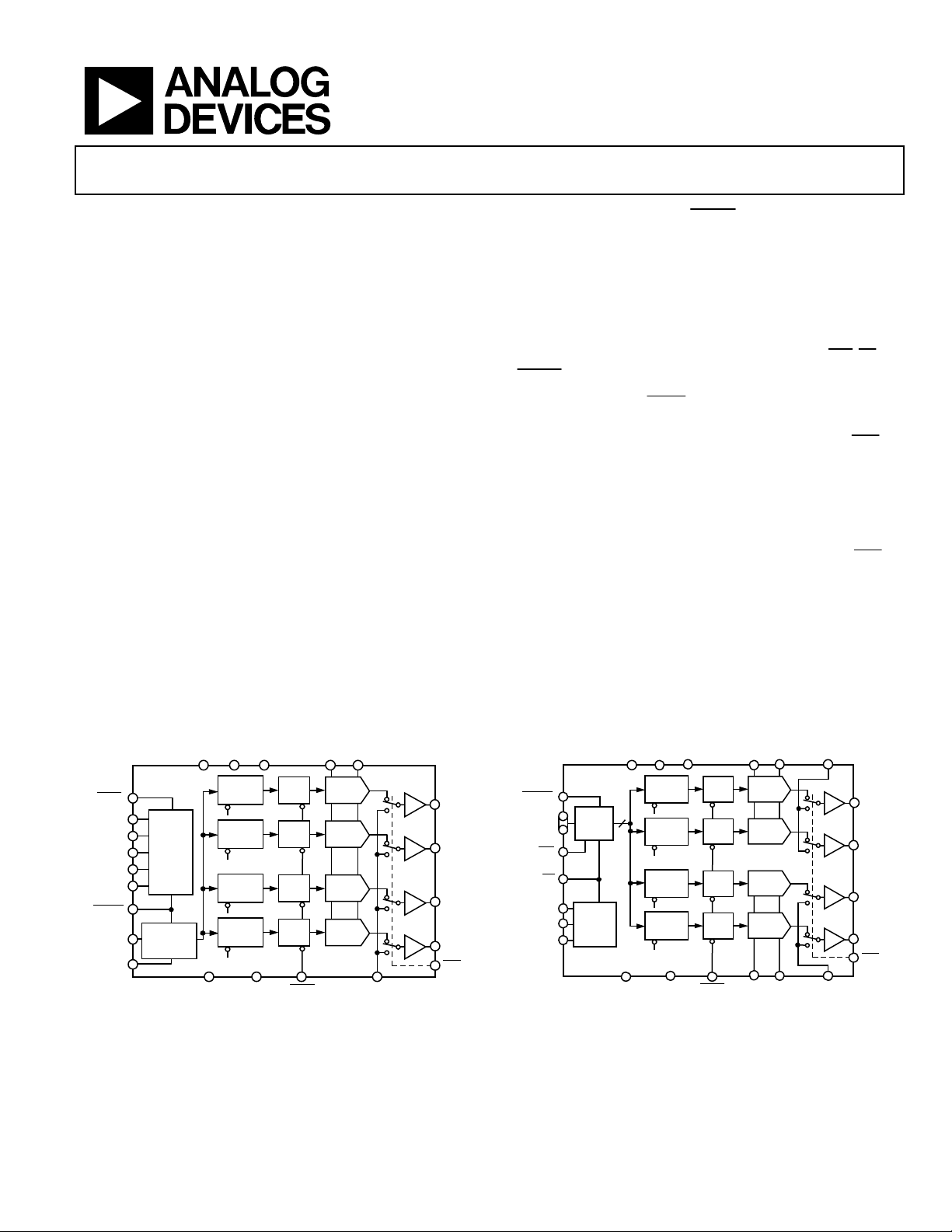
FUNCTIONAL BLOCK DIAGRAMS
(–)
VDDV
PAE N
PA0
PA1
PA2
PA3
PA4
FSYNC
DIN
SCLK
AD7834
CONTROL
LOGIC
AND
ADDRESS
DECODE
SERIAL-TO-
PARALLEL
CONVERTER
CC
AGND DGND DSG
INPUT
REGI STER
1
INPUT
REGISTER
2
INPUT
REGISTER
3
INPUT
REGISTER
4
SS
DAC 1
LATCH
DAC 2
LATCH
DAC 3
LATCH
DAC 4
LATCH
LDAC
Figure 1. AD7834 Figure 2. AD7835
Rev. D
Information furnished by Analog Devices is believed to be accurate and reliable. However, no
responsibility is assumed by Anal og Devices for its use, nor for any infringements of patents or ot her
rights of third parties that may result from its use. Specifications subject to change without notice. No
license is granted by implication or otherwise under any patent or patent rights of Analog Devices.
Trademarks and registered trademarks are the property of their respective owners.
REF
DAC 1
DAC 2
DAC 3
DAC 4
V
(+)
REF
×1
V
OUT
×1
V
OUT
V
×1
OUT
×1
V
OUT
CLR
(–)
REF
AD7835
1
2
3
4
BYSHF
DB13
01006-001
DB0
WR
CS
INPUT
BUFFER
A0
ADDRESS
A1
DECODE
A2
INPUT
REGISTER
1
14
INPUT
REGISTER
2
INPUT
REGISTER
3
INPUT
REGISTER
4
AGND DGND
DAC 1
LATCH
DAC 2
LATCH
DAC 3
LATCH
DAC 4
LATCH
LDAC
V
REF
DAC 3
(–)B
DAC 1
DAC 2
DAC 4
(+)
DSGA
REF
×1
V
1
OUT
×1
V
2
OUT
×1
V
3
OUT
×1
DSGB
(+)B
V
REF
V
OUT
CLR
4
01006-002
One Technology Way, P.O. Box 9106, Norwood, MA 02062-9106, U.S.A.
Tel: 781.329.4700
Fax: 781.461.3113 ©2003–2007 Analog Devices, Inc. All rights reserved.
www.analog.com

AD7834/AD7835
TABLE OF CONTENTS
Features.............................................................................................. 1
Applications....................................................................................... 1
General Description ......................................................................... 1
Functional Block Diagrams............................................................. 1
Revision History ............................................................................... 2
Specifications..................................................................................... 3
AC Performance Characteristics ................................................ 5
Timing Specifications .................................................................. 6
Absolute Maximum Ratings............................................................ 7
Thermal Resistance ...................................................................... 7
ESD Caution.................................................................................. 7
Pin Configurations and Function Descriptions ........................... 8
Typical Performance Characteristics ........................................... 11
Terminology .................................................................................... 13
Theory of Operation ...................................................................... 14
DAC Architecture....................................................................... 14
Data Loading—AD7834 Serial Input Device ......................... 14
Data Loading—AD7835 Parallel Loading Device .................14
Unipolar Configuration............................................................. 15
Bipolar Configuration................................................................ 16
Controlled Power-On of the Output Stage.................................. 17
Power-On with
Power-On with
Loading the DAC and Using the
DSG Voltage Range .................................................................... 18
Power-On of the AD7834/AD7835.............................................. 19
Microprocessor Interfacing........................................................... 20
AD7834 to 80C51 Interface ...................................................... 20
AD7834 to 68HC11 Interface................................................... 20
AD7834 to ADSP-2101 Interface ............................................. 20
AD7834 to DSP56000/DSP56001 Interface............................ 21
AD7834 to TMS32020/TMS320C25 Interface....................... 21
Interfacing the AD7835—16-Bit Interface.............................. 21
Interfacing the AD7835—8-Bit Interface................................ 22
Applications Information.............................................................. 23
Serial Interface to Multiple AD7834s ...................................... 23
Opto-Isolated Interface ............................................................. 23
Automated Test Equipment ...................................................... 23
Power Supply Bypassing and Grounding................................ 24
Outline Dimensions....................................................................... 25
Ordering Guide .......................................................................... 27
CLR
LDAC
Low,
Low,
LDAC
High................................... 17
CLR
High................................... 17
CLR
Input .......................... 17
REVISION HISTORY
7/07—Rev. C to Rev. D
Changes to Table 5 ........................................................................... 7
Added Table 6.................................................................................... 7
Changes to Table 8............................................................................ 9
Updated Outline Dimensions....................................................... 25
Changes to Ordering Guide.......................................................... 27
7/05—Rev. B to Rev. C
Updated Format..................................................................Universal
Changes to Figure 40...................................................................... 25
Changes to Ordering Guide.......................................................... 27
7/03—Rev. A to Rev. B
Revision 0: Initial Version
Rev. D | Page 2 of 28

AD7834/AD7835
SPECIFICATIONS
1
= T
VCC = 5 V ± 5%; VDD = 15 V ± 5%; VSS = −15 V ± 5%; AGND = DGND = 0 V; T
A
MIN
to T
Table 1.
Parameter
A B S Unit Test Conditions/Comments
ACCURACY
Resolution 14 14 14 Bits
Relative Accuracy ±2 ±1 ±2 LSB max
Differential Nonlinearity ±0.9 ±0.9 ±0.9 LSB max Guaranteed monotonic over temperature.
Full-Scale Error V
T
to T
MIN
±5 ±5 ±8 mV max
MAX
Zero-Scale Error ±4 ±4 ±5 mV max V
Gain Error ±0.5 ±0.5 ±0.5 mV typ V
Gain Temperature
Coefficient
2
4 4 4 ppm FSR/°C typ
20 20 20 ppm FSR/°C max
DC Crosstalk2 50 50 50 μV max See the Terminology section. RL = 10 kΩ.
REFERENCE INPUTS
DC Input Resistance 30 30 30 MΩ typ
Input Current ±1 ±1 ±1 μA max Per input.
V
(+) Range 0/8.192 0/8.192 0/8.192 V min/max
REF
V
(−) Range −8.192/0 −8.192/0 −8.192/0 V min/max
REF
V
REF
(+) − V
(−) 5/14 7/14 5/14 V min/max
REF
DEVICE SENSE GROUND INPUTS
Input Current ±2 ±2 ±2 μA max Per input. V
DIGITAL INPUTS
V
, Input High Voltage 2.4 2.4 2.4 V min
INH
V
, Input Low Voltage 0.8 0.8 0.8 V max
INL
I
, Input Current ±10 ±10 ±10 μA max
INH
CIN, Input Capacitance 10 10 10 pF max
POWER REQUIREMENTS
VCC 5.0 5.0 5.0 V nom ±5% for specified performance.
VDD 15.0 15.0 15.0 V nom ±5% for specified performance.
VSS −15.0 −15.0 −15.0 V nom ±5% for specified performance.
Power Supply Sensitivity
ΔFull Scale/ΔVDD 110 110 110 dB typ
ΔFull Scale/ΔVSS 100 100 100 dB typ
ICC 0.2 0.2 0.5 mA max V
3 3 3 mA max AD7834: V
6 6 6 mA max AD7835: V
IDD 13 13 15 mA max AD7834: outputs unloaded.
15 15 15 mA max AD7835: outputs unloaded.
ISS 13 13 15 mA max Outputs unloaded.
1
Temperature range for A, B, and C versions is −40°C to +85°C.
2
Guaranteed by design.
, unless otherwise noted.
MAX
(+) = +7 V, V
REF
(+) = +7 V, V
REF
(+) = +7 V, V
REF
(−) = −7 V.
REF
(−) = −7 V.
REF
(−) = −7 V.
REF
For specified performance. Can go as low as
0 V, but performance is not guaranteed.
= −2 V to +2 V.
DSG
= VCC, V
INH
= DGND.
INL
= 2.4 V min, V
INH
= 2.4 V min, V
INH
= 0.8 V max.
INL
= 0.8 V max.
INL
Rev. D | Page 3 of 28

AD7834/AD7835
VCC = 5 V ± 5%; VDD = 12 V ± 5%; VSS = −12 V ± 5%; AGND = DGND = 0 V; T
1
= T
to T
MIN
A
, unless otherwise noted.
MAX
Table 2.
Parameter
A B S Unit Test Conditions/Comments
ACCURACY
Resolution 14 14 14 Bits
Relative Accuracy ±2 ±1 ±2 LSB max
Differential Nonlinearity ±0.9 ±0.9 ±0.9 LSB max Guaranteed monotonic over temperature.
Full-Scale Error V
T
to T
MIN
±5 ±5 ±8 mV max
MAX
Zero-Scale Error ±4 ±4 ±5 mV max V
Gain Error ±0.5 ±0.5 ±0.5 mV typ V
(+) = +5 V, V
REF
(+) = +5 V, V
REF
(+) = +5 V, V
REF
(−) = –5 V.
REF
(−) = −5 V.
REF
(−) = −5 V.
REF
Gain Temperature Coefficient2 4 4 4 ppm FSR/°C typ
20 20 20 ppm FSR/°C max
DC Crosstalk2 50 50 50 μV max See the Terminology section. RL = 10 kΩ.
REFERENCE INPUTS
DC Input Resistance 30 30 30 MΩ typ
Input Current ±1 ±1 ±1 μA max Per input.
V
(+) Range 0/8.192 0/8.192 0/8.192 V min/max
REF
V
(−) Range −5/0 −5/0 −5/0 V min/max
REF
V
REF
(+) − V
(−) 5/13.192 7/13.192 5/13.192 V min/max
REF
For specified performance. Can go as low as
0 V, but performance is not guaranteed.
DEVICE SENSE GROUND INPUTS
Input Current ±2 ±2 ±2 μA max Per input. V
= −2 V to +2 V.
DSG
DIGITAL INPUTS
V
, Input High Voltage 2.4 2.4 2.4 V min
INH
V
, Input Low Voltage 0.8 0.8 0.8 V max
INL
I
, Input Current ±10 ±10 ±10 μA max
INH
CIN, Input Capacitance 10 10 10 pF max
POWER REQUIREMENTS
VCC 5.0 5.0 5.0 V nom ±5% for specified performance.
VDD 15.0 15.0 15.0 V nom ±5% for specified performance.
VSS −15.0 −15.0 −15.0 V nom ±5% for specified performance.
Power Supply Sensitivity
ΔFull Scale/ΔVDD 110 110 110 dB typ
ΔFull Scale/ΔVSS 100 100 100 dB typ
ICC 0.2 0.2 0.5 mA max V
3 3 3 mA max AD7834: V
6 6 6 mA max AD7835: V
= VCC, V
INH
= DGND.
INL
= 2.4 V min, V
INH
= 2.4 V min, V
INH
= 0.8 V max.
INL
= 0.8 V max.
INL
IDD 13 13 15 mA max AD7834: outputs unloaded.
15 15 15 mA max AD7835: outputs unloaded.
ISS 13 13 15 mA max Outputs unloaded.
1
Temperature range for A, B, and C versions is −40°C to +85°C.
2
Guaranteed by design.
Rev. D | Page 4 of 28
AD7834/AD7835
AC PERFORMANCE CHARACTERISTICS
These characteristics are included for design guidance and are not subject to production testing.
Table 3.
Parameter
DYNAMIC PERFORMANCE
Output Voltage Settling Time 10 10 10 μs
Digital-to-Analog Glitch Impulse 120 120 120 nV-s
DC Output Impedance 0.5 0.5 0.5 Ω See the Terminology section.
Channel-to-Channel Isolation 100 100 100 dB See the Terminology section; applies to the AD7835 only.
DAC-to-DAC Crosstalk 25 25 25 nV-s See the Terminology section.
Digital Crosstalk 3 3 3 nV-s
Digital Feedthrough—AD7834 0.2 0.2 0.2 nV-s Effect of input bus activity on DAC output under test.
Digital Feedthrough—AD7835 1.0 1.0 1.0 nV-s
Output Noise Spectral Density at 1 kHz 40 40 40 nV/√Hz All 1s loaded to DAC. V
A B S Unit (typ) Test Conditions/Comments
Full-scale change to ±1/2 LSB. DAC latch contents
alternately loaded with all 0s and all 1s.
Measured with V
(+) = V
REF
REF
alternately loaded with all 0s and all 1s.
Feedthrough to DAC output under test due to change in
digital input code to another converter.
(+) = V
REF
(−) = 0 V. DAC latch
(−) = 0 V.
REF
Rev. D | Page 5 of 28
AD7834/AD7835
)
TIMING SPECIFICATIONS
VCC = 5 V ± 5%; VDD = 11.4 V to 15.75 V; VSS = −11.4 V to −15.75 V; AGND = DGND = 0 V1.
Table 4.
Parameter Limit at T
MIN
AD7834-SPECIFIC
2
t
1
2
t
2
2
t
30 ns min SCLK high time
3
30 ns min
t4
100 ns min SCLK cycle time
50 ns min SCLK low
t5 40 ns min
t6 30 ns min Data setup time
10 ns min Data hold time
t7
0 ns min
t8
t9 40 ns min
t21 20 ns min Delay between write operations
AD7835-SPECIFIC
t11 15 ns min
t12 15 ns min
t13 0 ns min
t14 0 ns min
t15 40 ns min
t16 40 ns min Data setup time
10 ns min Data hold time
t17
0 ns min
t18
t19 0 ns min
t20 0 ns min
GENERAL
t10 40 ns min
1
All input signals are specified with tr = tf = 5 ns (10% to 90% of 5 V) and time from a voltage level of 1.6 V.
2
Rise and fall times should be no longer than 50 ns.
1ST
SCLK
FSYNC
DIN
(SIMULTANEOUS
LDAC
UPDATE)
LDAC
(PER-CHANNE L
UPDATE
2ND
CLK
CLK
t
4
t
6
t
MSB LSB
7
D23 D2 2
t
8
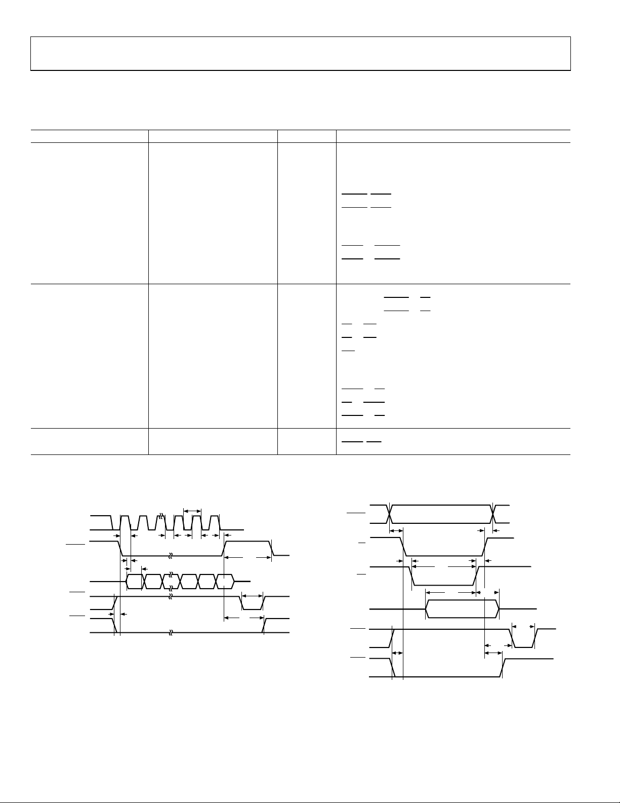
Figure 3. AD7834 Timing Diagram Figure 4. AD7835 Timing Diagram
t
1
t
2
Unit Description
, T
MAX
24TH
CLK
t
3
t
5
t
21
D0
D1
t
10
t
9
01006-003
(SIMULTANEOUS
(PER-CHANNEL
, PAEN setup time
FSYNC
, PAEN hold time
FSYNC
LDAC
to FSYNC setup time
to FSYNC hold time
LDAC
A0, A1, A2, BYSHF
A0, A1, A2, BYSHF
CS
to WR setup time
CS
to WR hold time
WR
pulse width
LDAC
to CS setup time
CS
to LDAC setup time
to CS hold time
LDAC
LDAC
, CLR pulse width
A0 A1 A2
BYSHF
CS
WR
DB0 TO DB13
LDAC
UPDATE)
LDAC
UPDATE)
to CS setup time
to CS hold time
t
11
t
13
t
18
t
15
t
16
t
12
t
14
t
17
t
10
t
19
t
20
01006-004
Rev. D | Page 6 of 28
AD7834/AD7835
ABSOLUTE MAXIMUM RATINGS
TA = 25°C unless otherwise noted. Transient currents of up to 100 mA do not cause SCR latch-up. VCC must not exceed VDD by more than
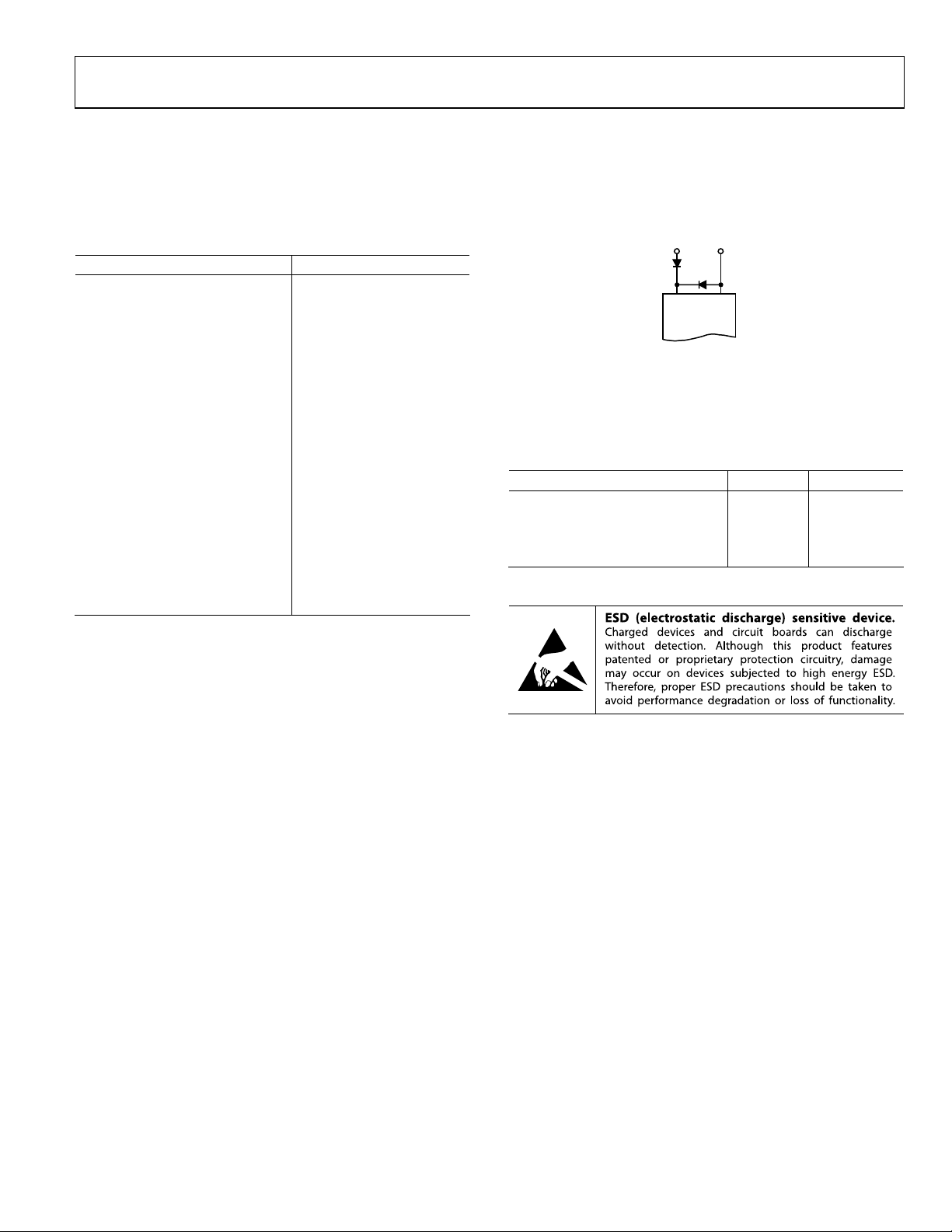
0.3 V. If it is possible for this to happen during power supply sequencing, the diode protection scheme shown in
provide protection.
V
Table 5.
Parameter Rating
VCC to DGND −0.3 V to +7 V, or VDD + 0.3 V
(whichever is lower)
VDD to AGND −0.3 V to +17 V
DD
IN4148
SD103C
V
DD
AD7834/
AD7835
VSS to AGND +0.3 V to –17 V
AGND to DGND −0.3 V to +0.3 V
Figure 5. Diode Protection
−0.3 V to VCC + 0.3 V Digital Inputs to DGND
V
(+) to V
REF
V
(+) to AGND VSS – 0.3 V to VDD + 0.3 V
REF
V
(–) to AGND VSS – 0.3 V to VDD + 0.3 V
REF
(–) −0.3 V to +18 V
REF
VSS – 0.3 V to VDD + 0.3 V DSG to AGND
V
(1–4) to AGND VSS – 0.3 V to VDD + 0.3 V
OUT
Operating Temperature Range, T
A
−40°C to +85°C Industrial (A Version)
−65°C to +150°C Storage Temperature Range
150°C Junction Temperature, TJ (max)
Power Dissipation, PD (max) (TJ − TA)/θJA
Lead Temperature JEDEC Industry Standard
Soldering J-STD-020
THERMAL RESISTANCE
θJA is specified for the worst-case conditions, that is, a device
soldered in a circuit board for surface-mount packages.
Table 6. Thermal Resistance
Package Type θJA Unit
PDIP 75 °C/W
SOIC 75
MQFP 95
PLCC 55 °C/W
ESD CAUTION
Stresses above those listed under Absolute Maximum Ratings
may cause permanent damage to the device. This is a stress
rating only; functional operation of the device at these or any
other conditions above those indicated in the operational
section of this specification is not implied. Exposure to absolute
maximum rating conditions for extended periods may affect
device reliability.
Figure 5 can be used to
V
CC
V
CC
01006-005
°C/W
°C/W
Rev. D | Page 7 of 28
AD7834/AD7835
PIN CONFIGURATIONS AND FUNCTION DESCRIPTIONS
28
27
26
25
24
23
22
21
20
19
18
17
16
15
AGND
NC
NC
NC
NC
V
DD
V
OUT
V
OUT
CLR
LDAC
FSYNC
PAEN
PA4
PA3
1
3
01006-006
V
REF
V
REF
V
V
DGND
SCLK
V
DSG
OUT
OUT
V
DIN
PA0
PA1
PA2
SS
(–)
(+)
NC
2
4
CC
1
2
3
4
5
AD7834
6
TOP VIEW
(Not to Scale)
7
8
9
10
11
12
13
14
NC = NO CONNECT
Figure 6. AD7834 PDIP and SOIC Pin Configuration
Table 7. AD7834 Pin Function Descriptions
Pin No. Pin Mnemonic Description
1 VSS Negative Analog Power Supply: −15 V ± 5% or −12 V ± 5%.
2 DSG
3 V
4 V
(−) Negative Reference Input. The negative reference voltage is referred to AGND.
REF
Positive Reference Input. The positive reference voltage is referred to AGND.
(+)
REF
5, 24, 25, 26, 27 NC
V
OUT
1 to V
OUT
4
8 DGND
9 VCC
Logic Power Supply: 5 V ± 5%.
10 SCLK
Device Sense Ground Input. Used in conjunction with the CLR
the DACs. When CLR
is low, the DAC outputs are forced to the potential on the DSG pin.
No Connect.
22, 6, 21, 7 DAC Outputs.
Digital Ground.
Clock Input. Used for writing data to the device; data is clocked into the input register on the
falling edge of SCLK.
11 DIN
12,13,14,15,16 PA0 to PA4
Serial Data Input.
Package Address Inputs. These inputs are hardwired high (VCC) or low (DGND) to assign dedicated
package addresses in a multipackage environment.
17
PAEN
Package Address Enable Input. When low, this input allows normal operation of the device. When
high, the device ignores the package address, but not the channel address, in the serial data
stream and loads the serial data into the input registers. This feature is useful in a multipackage
application where it can be used to load the same data into the same channel in each package.
18
Frame Sync Input. Active low logic input used, in conjunction with DIN and SCLK, to write data to
FSYNC
the device with serial data expected after the falling edge of this signal. The contents of the 24-bit
serial-to-parallel input register are transferred on the rising edge of this signal.
19
Load DAC Input (Level Sensitive). This input signal, in conjunction with the FSYNC input signal,
LDAC
LDAC
determines how the analog outputs are updated. If
is maintained high while new data is
being loaded into the device’s input registers, no change occurs on the analog outputs.
Subsequently, when
LDAC
is brought low, the contents of all four input registers are transferred
into their respective DAC latches, updating all of the analog outputs simultaneously.
20
CLR
Asynchronous Clear Input (Level Sensitive, Active Low). When this input is brought low, all analog
outputs are switched to the externally set potential on the DSG pin. When CLR
signal outputs remain at the DSG potential until LDAC
is brought low. When LDAC is brought low,
the analog outputs are switched back to reflect their individual DAC output levels. As long as CLR
LDAC
remains low, the
potential on the DSG pin.
signals are ignored, and the signal outputs remain switched to the
23 VDD Positive Analog Power Supply: 15 V ± 5% or 12 V ± 5%.
28 AGND Analog Ground.
input for power-on protection of
is brought high, the
Rev. D | Page 8 of 28
AD7834/AD7835
AGND
DB2
NC
DB3
(+)B
V
DB4
NC
1
DSGA
2
1
V
3
OUT
2
V
4
OUT
NC
5
A2
6
A1
7
8
A0
CLR
9
LDAC
10
11
BYSHF
NC = NO CONNECT
(+)A
(–)A
REF
NC
V
PIN 1
IDENTIFIER
REF
V
DD
SS
V
V
NC
40 39 3841424344 36 35 3437
AD7835
TOP VIEW
(Not to Scale)
12 13 14 15 16 17 18 192021 22
CC
CS
WR
V
DB0
DGND
DB1
Figure 7. AD7835 MQFP Pin Configuration Figure 8. AD7835 PLCC Pin Configuration
Table 8. AD7835 Pin Function Descriptions
Pin No.
MQFP
1, 5, 33, 34,
37, 41, 44
Pin No. PLCC Pin Mnemonic Description
3, 6, 7, 11, 39,
NC No Connect.
40, 43
(–)A
(–)B
REF
REF
V
NC
NC
DSGA
V
OUT
V
OUT
CLR
LDAC
BYSHF
NC
A0
7
8
1
9
10
2
11
A2
12
13
A1
14
15
16
17
DB5
DB6
NC
33
32
DSGB
3
V
31
OUT
4
30
V
OUT
DB13
29
DB12
28
27
DB11
DB10
26
25
DB9
24
DB8
23
DB7
01006-007
NC = NO CONNECT
(+)A
REF
NC
V
SS
DD
V
AGND
V
244345642414043
1
PIN 1
IDENTIFIER
NC
REF
V
AD7835
TOP VIEW
(Not to Scale)
181920 21 22 23 24 252627 28
CC
CS
WR
V
DGND
DB0
DB1
DB2
NC
DB3
(+)B
REF
V
DB4
(–)B
REF
V
DB5
NC
DB6
NC
39
38
DSGB
3
V
37
OUT
36
4
V
OUT
DB13
35
34
DB12
33
DB11
DB10
32
31
DB9
DB8
30
29
DB7
01006-008
2 8 DSGA
Device Sense Ground A Input. Used in conjunction with the CLR
protection of the DACs. When
V
1 to V
OUT
8, 7, 6 14, 13, 12 A0, A1, A2
potential on the DSGA pin.
4 3, 4, 31, 30 9, 10, 37, 36 DAC Outputs.
OUT
Address Inputs. A0 and A1 are decoded to select one of the four input latches for a data
transfer. A2 is used to select all four DACs simultaneously.
9 15
CLR
Asynchronous Clear Input (Level Sensitive, Active Low). When this input is brought low,
all analog outputs are switched to the externally set potentials on the DSG pins (V
and V
2 follow DSGA, and V
OUT
signal outputs remain at the DSG potentials until LDAC
brought low, the analog outputs are switched back to reflect their individual DAC output
levels. As long as
remains low, the LDAC signals are ignored, and the signal outputs
CLR
remain switched to the potential on the DSG pins.
10 16
Load DAC Input (Level Sensitive). This input signal, in conjunction with the WR and CS
LDAC
input signals, determines how the analog outputs are updated. If
high while new data is being loaded into the device’s input registers, no change occurs
on the analog outputs. Subsequently, when
input registers are transferred into their respective DAC latches, updating the analog
outputs simultaneously. Alternatively, if
entered, the addressed DAC latch and corresponding analog output are updated
immediately on the rising edge of
11 17
Byte Shift Input. When low, it shifts the data on DB0 to DB7 into the DB8 to DB13 half of
BYSHF
the input register.
12 18
CS
Level-Triggered Chip Select Input (Active Low). The device is selected when this input is
low.
13 19
Level-Triggered Write Input (Active Low). When active, it is used in conjunction with CS
WR
to write data over the input databus.
14 20 VCC Logic Power Supply: 5 V ± 5%.
15 21 DGND Digital Ground.
CLR
is low, DAC outputs V
OUT
3 and V
4 follow DSGB). When CLR
OUT
LDAC
LDAC
.
WR
input for power-on
1 and V
OUT
2 are forced to the
OUT
OUT
is brought high, the
is brought low. When LDAC is
LDAC
is maintained
is brought low, the contents of all four
is brought low while new data is being
1
Rev. D | Page 9 of 28

AD7834/AD7835
Pin No.
MQFP
16 to 29 22 to 35 DB0 to DB13
32 38 DSGB
36, 35 42, 41 V
38 44 AGND Analog Ground.
39 1 VDD Positive Analog Power Supply: 15 V ± 5% or 12 V ± 5%.
40 2 VSS Negative Analog Power Supply: −15 V ± 5% or −12 V ± 5%.
42, 43 4, 5 V
Pin No. PLCC Pin Mnemonic Description
Parallel Data Inputs. The AD7835 can accept a straight 14-bit parallel word on DB0 to
DB13, where DB13 is the MSB and the
Alternatively for byte loading, the bottom eight data inputs, DB0 to DB7, are used for
data loading, and the top six data inputs, DB8 to DB13, should be hardwired to a logic
low. The
BYSHF
into the device.
Device Sense Ground B Input. Used in conjunction with the CLR
protection of the DACs. When
potential on the DSGB pin.
REF
REF
(+)B, V
(+)A, V
(−)B Reference Inputs for DACs 3 and 4. These reference voltages are referred to AGND.
REF
(−)A Reference Inputs for DAC 1 and DAC 2. These reference voltages are referred to AGND.
REF
input is hardwired to a logic high.
BYSHF
control input selects whether 8 LSBs or 6 MSBs of data are being loaded
CLR
is low, DAC outputs V
OUT
input for power-on
3 and V
4 are forced to the
OUT
Rev. D | Page 10 of 28

AD7834/AD7835
TYPICAL PERFORMANCE CHARACTERISTICS
1.0
0.8
0.6
0.4
0.2
0
INL (LSB)
–0.2
–0.4
–0.6
–0.8
–1.0
01
4 8 10 12 14
62
CODE/1000
01006-009
6
Figure 9. Typical INL Plot
0.50
0.45
0.40
INL (LSB)
0.35
0.30
0.25
0.20
0.15
0.10
0.05
0
DAC 3
DAC 2
TEMP = 25°C
ALL DACs FROM 1 DEVICE
Figure 12. Typical INL vs. V
DAC 1
DAC 4
01006-012
V
(+) (V)
REF
(+), V
(+) – V
REF
REF
(−) = 5 V
REF
8.00 2.5 5.0
0.5
0.4
0.3
0.2
0.1
0
DNL (LSB)
–0.1
–0.2
–0.3
–0.4
–0.5
01
CODE/1000
64 8 10 12 1462
01006-010
Figure 10. Typical DNL Plot
0.9
0.8
0.7
0.6
0.5
0.4
INL (LSB)
0.3
0.2
0.1
0
173
Figure 11. Typical INL vs. V
V
(+) (V)
REF
(+), V
REF
(−) = −6 V
REF
802456
01006-011
0.8
ALL DACs FROM ONE DEVI CE
0.7
0.6
DAC 3
0.5
0.4
INL (LSB)
0.3
0.2
0.1
0
–40 25
Figure 13. Typical INL vs. Temperature
1.0
0.8
0.6
0.4
0.2
0
DAC (LSB)
–0.2
–0.4
–0.6
–0.8
–1.0
014 8 10 12 1462
Figure 14. Typical DAC-to-DAC Matching
TEMPERATURE (°C)
CODE/1000
DAC 1
DAC 4
DAC 2
01006-013
85
01006-014
6
Rev. D | Page 11 of 28

AD7834/AD7835
–
VOLTS
–0.1
–0.2
8
6
4
2
VOLTS
0
0.7
0.6
0.5
0.4
0.3
0.2
0.1
VERT = 100mV/DIV
HORIZ = 1μs/DIV
0
Figure 15. Typical Digital/Analog Glitch Impulse
VERT = 2V/DIV
HORIZ = 1.2μs/DIV
(+) = +7V
V
REF
(–) = –3V
V
REF
7.250
7.225
7.200
7.175
7.150
01006-015
VOLTS
8
6
4
V
(+) = +7V
2
VOLTS
0
–2
–4
REF
V
(–) = –3V
REF
VERT = 2V/DIV
HORIZ = 1µs/DI V
VERT = 10mV/DIV
HORIZ = 1µs/DIV
2.985
–3.005
–3.025
–3.045
–3.065
–3.085
–3.105
VOLTS
01006-017
Figure 17. Settling Time(−)
–2
–4
VERT = 25mV/DIV
HORIZ = 2.5μs/DIV
7.125
7.100
01006-016
Figure 16. Settling Time(+)
Rev. D | Page 12 of 28

AD7834/AD7835
TERMINOLOGY
Relative Accuracy
Relative accuracy or endpoint linearity is a measure of the
maximum deviation from a straight line passing through the
endpoints of the DAC transfer function. It is measured after
adjusting for zero error and full-scale error. It is normally
expressed in LSBs or as a percentage of full-scale reading.
Differential Nonlinearity
Differential nonlinearity is the difference between the measured
change and the ideal 1 LSB change between any two adjacent
codes. A specified differential nonlinearity of 1 LSB maximum
ensures monotonicity.
DC Crosstalk
Although the common input reference (IR) voltage signals are
internally buffered, small IR drops in individual DAC reference
inputs across the die mean that an update to one channel
produces a dc output change in one or more channel outputs.
The four DAC outputs are buffered by op amps sharing
common V
and VSS power supplies. If the dc load current
DD
changes in one channel due to an update, a further dc change
occurs in one or more of the channel outputs. This effect is
most obvious at high load currents and is reduced as the load
currents are reduced. With high impedance loads, the effect is
virtually unmeasurable.
Output Voltage Settling Time
This is the amount of time it takes for the output to settle to a
specified level for a full-scale input change.
Digital-to-Analog Glitch Impulse
This is the amount of charge injected into the analog output
when the inputs change state. It is specified as the area of the
glitch in nV-secs. It is measured with the reference inputs
connected to 0 V and the digital inputs toggled between all
1s and all 0s.
Channel-to-Channel Isolation
Channel-to-channel isolation refers to the proportion of input
signal from the reference input of one DAC that appears at the
output of the other DAC. It is expressed in decibels (dB). The
AD7834 has no specification for channel-to-channel isolation
because it has one reference for all DACs. Channel-to-channel
isolation is specified for the AD7835.
DAC-to-DAC C rosst a l k
DAC-to-DAC crosstalk is defined as the glitch impulse that
appears at the output of one converter due to both the digital
change and the subsequent analog output (O/P) change at
another converter. It is specified in nV-secs.
Digital Crosstalk
The glitch impulse transferred to the output of one converter
due to a change in digital input code to the other converter is
defined as the digital crosstalk and is specified in nV-secs.
Digital Feedthrough
When the device is not selected, high frequency logic activity
on its digital inputs can be capacitively coupled both across and
through the device to show up as noise on the V
pins. This
OUT
noise is digital feedthrough.
DC Output Impedance
DC output impedance is the effective output source resistance.
It is dominated by package lead resistance.
Full-Scale Error
Full-scale error is the error in DAC output voltage when all 1s
are loaded into the DAC latch. Ideally, the output voltage, with
all 1s loaded into the DAC latch, should be V
(+) – 1 LSB.
REF
Full-scale error does not include zero-scale error.
Zero-Scale Error
Zero-scale error is the error in the DAC output voltage when
all 0s are loaded into the DAC latch. Ideally, the output voltage,
with all 0s in the DAC latch, is equal to V
(−). Zero-scale
REF
error is due mainly to offsets in the output amplifier.
Gain Error
Gain error is defined as (full-scale error) − (zero-scale error).
Rev. D | Page 13 of 28

AD7834/AD7835
THEORY OF OPERATION
DAC ARCHITECTURE
Each channel consists of a segmented 14-bit R-2R voltage-mode
DAC. The full-scale output voltage range is equal to the entire
reference span of V
binary; all 0s produce an output of V
output of V
REF
The analog output voltage of each DAC channel reflects the
contents of its own DAC latch. Data is transferred from the
external bus to the input register of each DAC latch on a per
channel basis. The AD7835 has a feature whereby the A2 pin
data can be transferred from the input databus to all four input
registers simultaneously.
Bringing the
to V
OUT
CLR
4, to the voltage level on the DSG pin. The signal
outputs are held at this level after the removal of the
and do not switch back to the DAC outputs until the
signal is exercised.
DATA LOADING—AD7834 SERIAL INPUT DEVICE
A write operation transfers 24 bits of data to the AD7834. The
first 8 bits are control data and the remaining 16 bits are DAC
data (see
nel to be updated with new data and which of 32 possible
packages the DAC resides in. In any communication with the
device, the first 8 bits must always be control data.
The DAC output voltages, V
reflect new data in the DAC input registers in one of two ways.
The first method normally keeps
LDAC
eously with the contents of their respective input registers. The
second method ties
a per channel basis after new data has been clocked into the
AD7834. With
the new data directly into the DAC latch, updating the analog
output voltage.
Data being shifted into the AD7834 enters a 24-bit long shift
register. If more than 24 bits are clocked in before
high, the last 24 bits transmitted are used as the control data
and DAC data.
Individual bit functions are shown in Figure 18.
D23
D23 determines whether the following 23 bits of address and
data should be used or ignored. This is effectively a software
chip select bit. D23 is the first bit to be transmitted in the 24-bit
long word.
Figure 18). The control data identifies the DAC chan-
low momentarily to update all DAC latches simultan-
(+) – V
REF
(−). The DAC coding is straight
REF
(−); all 1s produce an
REF
(+) − 1 LSB.
line low switches all the signal outputs, V
OUT
LDAC
low and channel updating occurs on
LDAC
low, the rising edge of
1 to V
4, can be updated to
OUT
LDAC
high and only pulses
FSYNC
FSYNC
OUT
CLR
signal
LDAC
transfers
goes
Table 9. D23 Control
D23 Control Function
0 Ignore the following 23 bits of information.
1 Use the following 23 bits of address and data as normal.
D22 and D21
D22 and D21 are decoded to select one of the four DAC channels within a device, as shown in
Tabl e 10 .
Table 10. D22, D21 Control
D22 D21 Control Function
0 0 Select Channel 1
0 1 Select Channel 2
1
1 0 Select Channel 3
1 1 Select Channel 4
D20 to D16
D20 and D16 determine the package address. The five address
bits allow up to 32 separate packages to be individually decoded.
Successful decoding is accomplished when these five bits match
up with the five hardwired pins on the physical package.
D15 to D0
D15 and D0 provide DAC data to be loaded into the identified
DAC input register. This data must have two leading 0s followed
by 14 bits of data, MSB first. The MSB is in location D13 of the
24-bit data stream.
DATA LOADING—AD7835 PARALLEL LOADING DEVICE
Data is loaded into the AD7835 in either straight 14-bit wide
words or in two 8-bit bytes.
BYSHF
In systems that transfer 14-bit wide data, the
should be hardwired to V
. This sets up the AD7835 as a
CC
straight 14-bit parallel-loading DAC.
In 8-bit bus systems where it is required to transfer data in two
bytes, it is necessary to have the
BYSHF
input under logic control.
In such a system, the top six pins of the device databus, DB8 to
DB13, must be hardwired to DGND. New low byte data is
loaded into the lower eight places of the selected input register
by carrying out a write operation while holding
A second write operation is subsequently executed with
low and the 6 MSBs on the DB0 to DB5 inputs (DB5 = MSB).
input
BYSHF
high.
BYSHF
Rev. D | Page 14 of 28

AD7834/AD7835
CONTROL BIT TO USE/IGNORE
FOLLOWING 23 BITS OF INFORMATION
CHANNEL ADDRESS MSB, D1
CHANNEL ADDRESS LSB, D2
PACKAGE ADDRESS MSB, PA4
PACKAGE ADDRESS, PA3
PACKAGE ADDRESS, PA2
PACKAGE ADDRESS, PA1
PACKAGE ADDRESS LSB, PA0
NOTE: D23IS THE FIRST BIT TRANSMITTED IN THE SERIAL WORD.
D23 D22 D21
D18 D17 D16 D15 D14 D13 D12 D11 D10 D9 D8 D7 D6 D5 D4 D3 D2 D1 D0
D20 D19
Figure 18. Bit Assignments for 24-Bit Data Stream of AD7834
When 14-bit transfers are being used, the DAC output voltages,
1 to V
V
OUT
4, can be updated to reflect new data in the DAC
OUT
input registers in one of two ways. The first method normally
keeps
LDAC
high and only pulses
LDAC
low momentarily to
update all DAC latches simultaneously with the contents of
their respective input registers. The second method ties
LDAC
low, and channel updating occurs on a per channel basis after
new data is loaded to an input register.
To avoid the DAC output going to an intermediate value during
a 2-byte transfer,
LDAC
should not be tied low permanently but
should be held high until the two bytes are written to the input
register. When the selected input register has been loaded with
the two bytes,
LDAC
should then be pulsed low to update the
DAC latch and, consequently, perform the digital-to-analog
conversion.
In many applications, it may be acceptable to allow the DAC
output to go to an intermediate value during a 2-byte transfer.
In such applications,
LDAC
can be tied low, thus using one less
control line.
The actual DAC input register that is being written to is determined by the logic levels present on the device address lines, as
shown in Tab l e 1 1 .
Table 11. AD7835—Address Line Truth Table
A2 A1 A0 DAC Selected
0 0 0 DAC 1
0 0 1 DAC 2
0 1 0 DAC 3
0 1 1 DAC 4
1 X X All DACs selected
UNIPOLAR CONFIGURATION
Figure 19 shows the AD7834/AD7835 in the unipolar binary
circuit configuration. The V
the
AD586, a 5 V reference. V
(+) input of the DAC is driven by
REF
(−) is tied to ground. Tab l e 1 2
REF
SECOND LEADING ZERO
FIRST LEADING ZERO
LSB, DB0
SECOND LSB, DB1
THIRD LSB, DB2
DB3
DB4
DB5
DB6
DB7
DB8
DB9
DB10
THIRD MSB, DB11
SECOND MSB,DB12
MSB, DB13
01006-018
gives the code table for unipolar operation of the AD7834/
AD7835.
+15V +5V
2
AD586
4
SIGNAL
GND
6
5
8
C1
1nF
1
ADDITIONAL PINS OMITTED FOR CLARITY
R1
10kΩ
V
REF
V
V
DD
(+)
AD7834/
AD7835
(–)
REF
V
–15V
SS
V
CC
V
1
AGND
DGND
OUT
V
(0V TO 5V)
SIGNAL
GND
OUT
Figure 19. Unipolar 5 V Operation
Offset and gain can be adjusted in Figure 19 as follows:
• To adjust offset, disconnect the V
load the DAC with all 0s, and adjust the V
until V
OUT
= 0 V.
(−) input from 0 V,
REF
(−) voltage
REF
• To adjust gain, load the AD7834/AD7835 with all 1s and
adjust R1 until V
= 5 V(16383/16384) = 4.999695 V.
OUT
Many circuits do not require these offset and gain adjustments.
In these circuits, R1 can be omitted. Pin 5 of the
left open circuit, and Pin 2 (V
(−)) of the AD7834/AD7835 is
REF
AD586 can be
tied to 0 V.
Table 12. Code Table for Unipolar Operation
1, 2
Binary Number in DAC Latch
MSB
00 0000 0000 0001 V
LSB Analog Output (V
V
(16383/16384) V
REF
V
(8192/16384) V 10 0000 0000 0000
REF
V
(8191/16384) V 01 1111 1111 1111
REF
(1/16384) V
REF
00 0000 0000 0000 0 V
1
V
= V
(+); VREF(−) = 0 V for unipolar operation.
REF
REF
2
For V
(+) = 5 V, 1 LSB = 5 V/214 = 5 V/16384 = 305 μV.
REF
01006-019
OUT
11 1111 1111 1111
)
Rev. D | Page 15 of 28

AD7834/AD7835
BIPOLAR CONFIGURATION
+15V
+5V
R1
39kΩ
6
4
7
C1
1μF
9
AD588
R2
100kΩ
100kΩ
1
ADDITIONAL PINS OMITTED FOR CLARITY
5
10
11
12 8
R3
2
3
V
1
14
15
16
13
REF
V
REF
Figure 20. Bipolar ±5 V Operation
Figure 20 shows the AD7834/AD7835 setup for ±5 V operation.
The
AD588 provides precision ±5 V tracking outputs that are
fed to the V
(+) and V
REF
(−) inputs of the AD7834/AD7835.
REF
The code table for bipolar operation of the AD7834/AD7835 is
shown in
Tabl e 1 3 .
Table 13. Code Table for Bipolar Operation
Binary Number in DAC Latch
MSB LSB Analog Output (V
11 1111 1111 1111
10 0000 0000 0001
10 0000 0000 0000
01 1111 1111 1111
00 0000 0000 0001
00 0000 0000 0000
1
V
= V
(+) – V
2
For V
REF
REF
(+) = +5 V and V
REF
(−).
REF
(−) = –5 V, 1 LSB = 10 V/214 = 10 V/16384 = 610 μV.
REF
V
REF
V
REF
V
REF
V
REF
V
REF
V
REF
V
DD
(+)
AD7834/
AD7835
(–)
–15V
(−) + V
(−) + V
(−) + V
(−) + V
(−) + V
(−) V
V
CC
V
OUT
1
AGND
DGND
V
SS
SIGNAL
1, 2
OUT
(16383/16384) V
REF
(8193/16384) V
REF
(8192/16384) V
REF
(8191/16384) V
REF
(1/16384) V
REF
V
OUT
(–5V TO +5V)
GND
)
01006-020
In Figure 20, full-scale and bipolar zero adjustments are
provided by varying the gain and balance on the
AD588. R2
varies the gain on the AD588 while R3 adjusts the offset of both
the +5 V and –5 V outputs together with respect to ground.
For bipolar-zero adjustment, the DAC is loaded with
1000 . . . 0000 and R3 is adjusted until V
= 0 V. Full scale
OUT
is adjusted by loading the DAC with all 1s and adjusting R2
until V
= 5(8191/8192) V = 4.99939 V.
OUT
When bipolar zero and full-scale adjustment are not needed, R2
and R3 are omitted. Pin 12 on the
AD588 should be connected to
Pin 11, and Pin 5 should be left floating.
Rev. D | Page 16 of 28

AD7834/AD7835
CONTROLLED POWER-ON OF THE OUTPUT STAGE
G
A block diagram of the output stage of the AD7834/AD7835 is
shown in
parallel with 200 pF. G
control the power-on voltage present at V
used in conjunction with the
Figure 21. It is capable of driving a load of 10 kΩ in
to G6 are transmission gates used to
1
. G1 and G2 are also
OUT
CLR
input to set V
to the user-
OUT
defined voltage present at the DSG pin.
G
DAC
1
G
3
G
2
DSG
G
5
G
6
G
4
R
V
OUT
01006-021
Figure 21. Block Diagram of AD7834/AD7835 Output Stage
POWER-ON WITH CLR
LOW, LDAC HIGH
The output stage of the AD7834/AD7835 is designed to allow
CLR
output stability during power-on. If
power-on, and power is applied to the part, G
open while G
, G3, and G5 are closed (see Figure 22).
2
G
DAC
1
G
3
G
2
DSG
G
5
is kept low during
, G4, and G6 are
1
G
6
G
4
R
V
OUT
01006-022
Figure 22. Output Stage with VDD < 10 V
V
is kept within a few hundred millivolts of DSG via G5
OUT
and R. R is a thin-film resistor between DSG and V
output amplifier is connected as a unity gain buffer via G
the DSG voltage is applied to the buffer input via G
. The
OUT
. The
2
, and
3
amplifier output is thus at the same voltage as the DSG pin. The
output stage remains configured as in
voltage at V
and VSS reaches approximately ±10 V. At this
DD
Figure 22 until the
point, the output amplifier has enough headroom to handle
signals at its input and has also had time to settle. The internal
power-on circuitry opens G
and G5 and closes G4 and G6 (see
3
Figure 23). As a result, the output amplifier is connected in
unity gain mode via G
to the noninverting input via G
and G6. The DSG voltage is still applied
4
. This voltage appears at V
2
OUT
.
DAC
V
is disconnected from the DSG pin by the opening of G5
OUT
but tracks the voltage present at DSG via the unity gain buffer.
POWER-ON WITH LDAC
In many applications of the AD7834/AD7835,
continuously low, updating the DAC after each valid data
transfer. If
G
is open, connecting the output of the DAC to the input of the
2
output amplifier. G
connecting the amplifier as a unity gain buffer, as before. V
connected to DSG via G
DSG and V
Then, the internal power-on circuitry opens G
closes G
and G6. This is the situation shown in Figure 24. At
4
this point, V
DAC
LOADING THE DAC AND USING THE CLR
LDAC
When
The voltage at V
put of the DAC. The output stage remains connected in this
manner until a
(see
Figure 23). Once again, V
DSG until
the unity gain buffer.
1
G
3
G
2
DSG
G
5
Figure 23. Output Stage with V
G
6
G
4
R
> 10 V and
DD
CLR
V
Low
OUT
LOW, CLR HIGH
LDAC
is kept
LDAC
is low when power is applied, G1 is closed and
and G5 are closed and G4 and G6 are open,
3
and R (a thin-film resistance between
5
) until VDD and VSS reach approximately ±10 V.
OUT
and G5 and
3
is at the same voltage as the DAC output.
OUT
G
1
G
G
2
DSG
G
5
Figure 24. Output Stage with
G
6
3
G
4
R
LDAC
Low
V
OUT
INPUT
goes low, it closes G1 and opens G2 as in Figure 24.
now follows the voltage present at the out-
OUT
CLR
signal is applied. Then, the situation reverts
remains at the same voltage as
OUT
LDAC
goes low. This reconnects the DAC output to
01006-023
OUT
01006-024
is
Rev. D | Page 17 of 28

AD7834/AD7835
DSG VOLTAGE RANGE
During power-on, the V
connected to the relevant DSG pins via G
resistor, R. The DSG potential must obey the maximum ratings
at all times. Thus, the voltage at DSG must always be within the
range V
at the V
– 0.3 V to VDD + 0.3 V. However, to keep the voltages
SS
pins of the AD7834/AD7835 within ±2 V of the
OUT
relevant DSG potential during power-on, the voltage applied to
DSG should also be kept within the range AGND – 2 V to
AGND + 2 V.
pins of the AD7834/AD7835 are
OUT
and the thin-film
6
Once the AD7834/AD7835 have powered on and the on-chip
amplifiers have settled, the situation is as shown in
Figure 23.
Any voltage subsequently applied to the DSG pin is buffered by
the same amplifier that buffers the DAC output voltage in
normal operation. Thus, for specified operations, the maximum
voltage applied to the DSG pin increases to the maximum
allowable V
DSG is the minimum V
(+) voltage, and the minimum voltage applied to
REF
(−) voltage. After the AD7834 or
REF
AD7835 has fully powered on, the outputs can track any DSG
voltage within this minimum/maximum range.
Rev. D | Page 18 of 28

AD7834/AD7835
POWER-ON OF THE AD7834/AD7835
Power is normally applied to the AD7834/AD7835 in the
following sequence: first V
V
(+) and V
REF
(−). The V
REF
power is applied to the part. V
(−) − 0.3 V. V
V
REF
V
is not allowed to go below VCC − 0.3 V.
DD
(−) is not allowed to go below VSS − 0.3 V.
REF
and VSS, then VCC, and then
DD
pins are not allowed to float when
REF
(+) is not allowed to go below
REF
In some systems, it is necessary to introduce one or more
Schottky diodes between pins to prevent the above situations
arising at power-on. These diodes are shown in
Figure 25.
However, in most systems, with careful consideration given to
power supply sequencing, the above rules are adhered to, and
protection diodes are not necessary.
1
ADDITIONAL PINS OMITTED FOR CLARITY
V
(+)
REF
AD7834
V
REF
1
(–)
SD103C
1N5711
1N5712
Figure 25. Power-On Protection
01006-025
Rev. D | Page 19 of 28

AD7834/AD7835
MICROPROCESSOR INTERFACING
AD7834 TO 80C51 INTERFACE
A serial interface between the AD7834 and the 80C51 microcontroller is shown in
of the AD7834, while RXD drives the serial data line of the part.
The 80C51 provides the LSB of its SBUF register as the first bit
in the serial data stream. The AD7834 expects the MSB of the
24-bit write first. Therefore, the user has to ensure that data in
the SBUF register is arranged correctly so the data is received
MSB first by the AD7834/AD7835. When data is to be transmitted to the part, P3.3 is taken low. Data on RXD is valid on
the falling edge of TXD. The 80C51 transmits its data in 8-bit
bytes with only eight falling clock edges occurring in the transmit cycle. To load data to the AD7834, P3.3 is left low after the
first 8 bits are transferred. A second byte is then transferred,
with P3.3 still kept low. After the third byte has been transferred, the P3.3 line is taken high.
80C51
1
ADDITIONAL PINS OMITTED FOR CLARITY
and
CLR
LDAC
port outputs. The user can bring
bytes have been transmitted to update the DAC, which has been
programmed. Alternatively, it is possible to wait until all the
input registers have been loaded (12-byte transmits) and then
update the DAC outputs.
AD7834 TO 68HC11 INTERFACE
Figure 27 shows a serial interface between the AD7834 and the
68HC11 microcontroller. SCK of the 68HC11 drives SCLK of
the AD7834, while the MOSI output drives the serial data line,
DIN, of the AD7834. The
Line PC7.
For correct operation of this interface, the 68HC11 should be
configured so that its CPOL bit is 0 and its CPHA bit is 1. When
data is to be transferred to the part, PC7 is taken low. When the
68HC11 is configured like this, data on MOSI is valid on the
falling edge of SCK. The 68HC11 transmits its serial data in 8-bit
bytes, MSB first. The AD7834 also expects the MSB of the 24-bit
write first. Eight falling clock edges occur in the transmit cycle.
Figure 26. TXD of the 80C51 drives SCLK
1
P3.5
P3.4
P3.3
TXD
RXD
Figure 26. AD7834 to 80C51 Interface
CLR
LDAC
FSYNC
SCLK
DIN
AD7834
1
01006-026
on the AD7834 are also controlled by 80C51
LDAC
low after every three
FSYNC
signal is derived from Port
To load data to the AD7834, PC7 is left low after the first eight
bits are transferred. A second byte of data is then transmitted
serially to the AD7834. Then, a third byte is transmitted and,
when this transfer is complete, the PC7 line is taken high.
AD7834
1
01006-027
1
ADDITIONAL PINS OMITTED FOR CLARITY
In Figure 27,
1
68HC11
PC5
PC6
PC7
SCK
MOSI
Figure 27. AD7834 to 68HC11 Interface
and
CLR
are controlled by the PC6 and PC5
LDAC
CLR
LDAC
FSYNC
SCLK
DIN
port outputs, respectively. As with the 80C51, each DAC of the
AD7834 can be updated after each 3-byte transfer, or all DACs
can be simultaneously updated after 12 bytes are transferred.
AD7834 TO ADSP-2101 INTERFACE
An interface between the AD7834 and the
Figure 28. In the interface shown, SPORT0 is used to transfer
in
data to the part. SPORT1 is configured for alternate functions.
FO, the flag output on SPORT0, is connected to
used to load the DAC latches. In this way, data is transferred
from the
ADSP-2101 to all the input registers in the DAC, and
the DAC latches are updated simultaneously. In the application
shown, the
CLR
pin on the AD7834 is controlled by circuitry
that monitors the power in the system.
POWER
MONITOR
ADSP-2101
1
ADDITIONAL PINS OMITTED FOR CLARITY
1
FO
TFS
SCK
DT
Figure 28. AD7834 to ADSP-2101 Interface
The AD7834 requires 24 bits of serial data framed by a single
FSYNC
pulse. It is necessary that this
all the data is transferred. This can be provided by the
in one of two ways. Both require setting the serial word length of
the SPORT to 12 bits, with the following conditions: internal
SCLK, alternate framing mode, and active low framing signal.
ADSP-2101 is shown
LDAC
AD7834
CLR
LDAC
FSYNC
SCLK
DIN
FSYNC
pulse stay low until
and is
1
01006-028
ADSP-2101
Rev. D | Page 20 of 28

AD7834/AD7835
First, data can be transferred using the autobuffering feature of
the
ADSP-2101, sending two 12-bit words directly after each
other. This ensures a continuous transmit frame synchronization (TFS ) pulse. Second, the first data word is loaded to the
serial port, the subsequent generated interrupt is trapped, and
then the second data word is sent immediately after the first.
Again, this produces a continuous TFS pulse that frames the
24 data bits.
AD7834 TO DSP56000/DSP56001 INTERFACE
Figure 29 shows a serial interface between the AD7834 and the
DSP56000/DSP56001. The serial port is configured for a word
length of 24 bits, gated clock, and FSL0 and FSL1 control bits
each set to 0. Normal mode synchronous operation is selected,
which allows the use of SC0 and SC1 as outputs controlling
CLR
be inverted before being applied to
and
LDAC
, respectively. The framing signal on SC2 has to
FSYNC
. SCK is internally
generated on the DSP56000/DSP56001 and is applied to SCLK
on the AD7834. Data from the DSP56000/DSP56001 is valid on
the falling edge of SCK.
DSP56000/
1
DSP56001
SC0
SC1
SC2
SCK
STD
1
ADDITIONAL PINS OMITTED FOR CLARITY
CLR
LDAC
FSYNC
SCLK
DIN
Figure 29. AD7834 to DSP56000/DSP56001 Interface
AD7834
1
01006-029
AD7834 TO TMS32020/TMS320C25 INTERFACE
A serial interface between the AD7834 and the TMS32020/
TMS320C25 DSP processor is shown in
CLKX and FSX signals for the TMS32020/TMS32025 are
generated using an external clock/timer circuit. The CLKX and
FSX pins are configured as inputs. The TMS32020/ TMS320C25
are set up for an 8-bit serial data length. Data can then be written
to the AD7834 by writing three bytes to the serial port of the
TMS32020/TMS320C25. In the configuration shown in
30
, the CLR input on the AD7834 is controlled by the XF output
on the TMS32020/TMS320C25. The clock/timer circuit controls
LDAC
the
input on the AD7834. Alternatively,
tied to ground to allow automatic update of the DAC latches after
each transfer.
Figure 30. The
LDAC
can also be
Figure
TMS32020/
TMS320C25
1
ADDITIONAL PINS OMITTED FOR CLARITY
1
XF
FSX
CLKX
DX
Figure 30. AD7834 to TMS32020/TMS320C25 Interface
INTERFACING THE AD7835—16-BIT INTERFACE
The AD7835 can be interfaced to a variety of microcontrollers
or DSP processors, both 8-bit and 16-bit.
AD7835 interfaced to a generic 16-bit microcontroller/DSP
Tabl e 1 1 .
DSP
PROCESSOR
DATABUS
UPPER BITS OF
ADDRESS BUS
BYSHF
is tied to VCC in this interface. The lower
1
D13
D0
A2
A1
A0
R/W
Figure 31. AD7835 16-Bit Interface
processor.
address lines from the processor are connected to A0, A1, and
A2 on the AD7835 as shown. The upper address lines are
decoded to provide a chip select signal for the AD7835. They
are also decoded, in conjunction with the lower address lines if
need be, to provide an
driven by an external timing circuit or just tied low. The data
lines of the processor are connected to the data lines of the
AD7835. Selection options available for the DACs are provided
in
MICROCONTROLLER/
1
ADDITIONAL PI NS OMIT TED FOR CL ARITY
CLOCK/
TIMER
LDAC
signal. Alternatively,
ADDRESS
DECODE
1
AD7834
LDAC
CLR
FSYNC
SCLK
DIN
Figure 31 shows the
LDAC
V
CC
AD7835
BYSHF
D13
D0
CS
LDAC
A2
A1
A0
WR
01006-030
can be
1
01006-031
Rev. D | Page 21 of 28

AD7834/AD7835
INTERFACING THE AD7835—8-BIT INTERFACE
Figure 32 shows an 8-bit interface between the AD7835 and
a generic 8-bit microcontroller/DSP processor. Pin D13 to
Pin D8 of the AD7835 are tied to DGND. Pin D7 to Pin D0 of the
processor are connected to Pin D7 to Pin D0 of the AD7835.
BYSHF
is driven by the A0 line of the processor. This maps the
DAC upper bits and lower bits into adjacent bytes in the processor address space.
the DACs in the AD7835. For example, if the base address for the
DACs in the processor address space is decoded by the upper
address bits to location HC000, then the upper and lower bits of
the first DAC are at locations HC000 and HC001, respectively.
MICROCONTROLLER/
DSP
PROCESSOR
DATABUS
UPPER BITS O F
ADDRESS BUS
1
ADDITIONAL PINS OMIT TED FOR CL ARITY
Table 1 4 shows the truth table for addressing
D13
1
D7
D0
A3
A2
A1
A0
R/W
Figure 32. AD7835 8-Bit Interface
DGND
ADDRESS
DECODE
D8
AD7835
D7
D0
CS
LDAC
A2
A1
A0
BYSHF
WR
1
When writing to the DACs, the lower eight bits must be written
first, followed by the upper six bits. The upper six bits should be
output on data lines D0 to D5. Once again, the upper address
lines of the processor are decoded to provide a
CS
signal. They
are also decoded in conjunction with lines A3 to A0 to provide
an
LDAC
signal. Alternatively,
LDAC
can be driven by an external timing circuit or, if it is acceptable to allow the DAC output
to go to an intermediate value between 8-bit writes,
LDAC
can
be tied low.
Table 14. DAC Channel Decoding, 8-Bit Interface
Processor Address Lines
A3 A2 A1 A0 DAC Selected
x X X 0 Upper 6 bits of all DACs
1 X X 1 Lower 8 bits of all DACs
0 0 0 0
0 0 0 1
0 0 1 0
0 0 1 1
0 1 0 0
0 1 0 1
0 1 1 0
Upper 6 bits, DAC 1
Lower 8 bits, DAC 1
Upper 6 bits, DAC 2
Lower 8 bits, DAC 2
Upper 6 bits, DAC 3
Lower 8 bits, DAC 3
Upper 6 bits, DAC 4
0 1 1 1 Lower 8-bits, DAC 4
01006-032
Rev. D | Page 22 of 28

AD7834/AD7835
V
APPLICATIONS INFORMATION
SERIAL INTERFACE TO MULTIPLE AD7834S
Figure 33 shows how the package address pins of the AD7834
are used to address multiple AD7834s. This figure shows only
10 devices, but up to 32 AD7834s can each be assigned a unique
address by hardwiring each of the package address pins to V
or DGND. Normal operation of the device occurs when
PA EN
CC
is low. When serial data is being written to the AD7834s, only
the device with the same package address as the package address
contained in the serial data accepts data into the input registers.
Conversely, if
PA EN
is high, the package address is ignored, and
the data is loaded into the same channel on each package.
The primary limitation with multiple packages is the output
update rate. For example, if an output update rate of 10 kHz is
required, 100 μs are available to load all DACs. Assuming a
serial clock frequency of 10 MHz, it takes 2.5 μs to load data to
one DAC. Thus, 40 DACs or 10 packages can be updated in this
time. As the update rate requirement decreases, the number of
possible packages increases.
1
MICROCONTRO LLER
CONTROL OUT
CONTROL OUT
SYNC OUT
SERIAL CLOCK O UT
SERIAL DATA OUT
1
ADDITIONAL PINS OMIT TED FOR CL ARITY
Figure 33. Serial Interface to Multiple AD7834s
AD7834
DEVICE 0
PAE N
LDAC
FSYNC
SCLK
DIN
AD7834
DEVICE 1
PAE N
LDAC
FSYNC
SCLK
DIN
AD7834
DEVICE 9
PAE N
LDAC
FSYNC
SCLK
DIN
PA0
PA1
PA2
PA3
PA4
1
PA0
PA1
PA2
PA3
PA4
1
PA0
PA1
PA2
PA3
PA4
V
CC
V
CC
01006-033
OPTO-ISOLATED INTERFACE
In many process control applications, it is necessary to provide
an isolation barrier between the controller and the unit being
controlled. Opto-isolators can provide voltage isolation in
excess of 3 kV. The serial loading structure of the AD7834
makes it ideal for opto-isolated interfaces because the number
of interface lines is kept to a minimum.
Figure 34 shows a 5-channel isolated interface to the AD7834.
Multiple devices are connected to the outputs of the opto-coupler
and controlled as for serial interfacing. To reduce the number of
opto-isolators, the
is not used. If the
PA EN
line doesn’t need to be controlled if it
PA EN
line is not controlled by the microcontroller, it should be tied low at each device. If simultaneous updating of the DACs is not required, the
LDAC
pin on each part can
be tied permanently low and another opto-isolator is not needed.
MICROCONTROLLER
CONTROL OUT
CONTROL OUT
SYNC OUT
SERIAL CLOCK OUT
SERIAL DATA OUT
Figure 34. Opto-Isolated Interface
CC
OPTO-COUPLER
TO PAEN s
TO LDACs
TO FSYNCs
TO SCLKs
TO DINs
01006-034
AUTOMATED TEST EQUIPMENT
The AD7834/AD7835 are particularly suited for use in an
automated test environment.
providing the necessary voltages for the pin driver and the
window comparator in a typical ATE pin electronics configuration. Two
AD588s are used to provide reference voltages for
the AD7835. In the configuration shown, the
configured so that the voltage at Pin 1 is 5 V greater than the
voltage at Pin 9 and the voltage at Pin 15 is 5 V less than the
voltage at Pin 9.
AD588
One
is used as a reference for DAC 1 and DAC 2. These
DACs are used to provide high and low levels for the pin driver.
The pin driver can have an associated offset. This can be nulled
by applying an offset voltage to Pin 9 of the
code 1000 . . . 0000 is loaded into the DAC 1 latch, and the pin
driver output is set to the DAC 1 output. The V
adjusted until 0 V appears between the pin driver output and
DUT GND. This causes both V
set with respect to AGND by an amount equal to V
However, the output of the pin driver varies from −5 V to +5 V
with respect to DUT GND as the DAC input code varies from
000 . . . 000 to 111 . . . 111. The V
the DSGA pin. When a clear is performed on the AD7835, the
output of the pin driver is 0 V with respect to DUT GND.
Figure 35 shows the AD7835
AD588s are
AD588. First, the
voltage is
OFFSET
(+)A and V
REF
voltage is also applied to
OFFSET
(−)A to be off-
REF
OFFSET
.
Rev. D | Page 23 of 28

AD7834/AD7835
V
1µF
1
ADDITIONAL P INS OMIT TED FOR CLARITY
13
13
10
11
12
1µF
4
6
8
7
4
6
8
+15V
AD588
10 11 12
+15V
AD588
7
–15V
–15V
162
9
162
DUT
GND
OFFSET
3
1
15
14
9
3
1
15
14
0.1µF
V
REF
V
REF
DSG A
AD7835
V
REF
V
REF
(+)A
(–)A
(+)B
(–)B
AGND
V
OUT
V
OUT
1
DSG B
V
OUT
V
OUT
WINDOW
COMPARATOR
+15V
1
PIN
DRIVER
2
–15V
DUT
GND
V
DUT
DUT
GND
3
4
TO TESTER
Figure 35. ATE Application
The other AD588 provides a reference voltage for DAC 3 and
DAC 4. These provide the reference voltages for the window
comparator shown in
nected to DUT GND. This causes V
Figure 35. Pin 9 of this AD588 is con-
(+)B and V
REF
(−)B to be
REF
referenced to DUT GND. As DAC 3 and DAC 4 input codes vary
from 000 . . . 000 to 111 . . . 111, V
3 and V
OUT
4 vary from −5 V
OUT
to +5 V with respect to DUT GND. DUT GND is also connected
to DSGB. When the AD7835 is cleared, V
OUT
3 and V
OUT
4 are
cleared to 0 V with respect to DUT GND.
Care must be taken to ensure that the maximum and minimum
voltage specifications for the AD7835 reference voltages are
followed as shown in
Figure 35.
POWER SUPPLY BYPASSING AND GROUNDING
In any circuit where accuracy is important, careful consideration of the power supply and ground return layout helps to
ensure the rated performance. The printed circuit boards on
which the AD7834/AD7835 are mounted should be designed so
the analog and digital sections are separated and confined to
certain areas of the boards. This facilitates the use of ground
planes that can be easily separated. A minimum etch technique
is generally best for ground planes because it gives the best
shielding. Digital and analog ground planes should be joined at
only one place.
If the AD7834/AD7835 are the only devices requiring an AGND
to DGND connection, then the ground planes should be connected
at the AGND and DGND pins of the AD7834/ AD7835. If the
AD7834/AD7835 are in a system where multiple devices require
an AGND to DGND connection, the connection can still be made
at one point only, a star ground point, which can be established as
close as possible to the AD7834/AD7835.
Digital lines running under the device must be avoided because
they couple noise onto the die. The analog ground plane can run
under the AD7834/AD7835 to avoid noise coupling. The power
supply lines of the AD7834/AD7835 can use as large a trace as
possible to provide low impedance paths and reduce the effects of
glitches on the power supply line. Fast switching signals, such as
clocks, should be shielded with digital ground to avoid radiating
noise to other parts of the board. These signals should never be
run near the analog inputs. Avoid crossover of digital and analog
01006-035
signals. Traces on opposite sides of the board should run at right
angles to each other. This reduces the effects of feedthrough
through the board. A microstrip method is best but not always
possible with a double-sided board. With this method, the
component side of the board is dedicated to ground plane while
signal traces are placed on the solder side.
The AD7834/AD7835 must have ample supply bypassing located
as close as possible to the package, ideally right up against the
Figure 36 shows the recommended capacitor values of
device.
10 μF in parallel with 0.1 μF on each of the supplies. The 10 μF
capacitors are the tantalum bead type. The 0.1 μF capacitor can
have low effective series resistance (ESR) and effective series
inductance (ESI), such as the common ceramic types, which
provide a low impedance path to ground at high frequencies to
handle transient currents due to internal logic switching.
V
V
CC
DGND
10μF
0.1μF
1
ADDITIONAL PINS OMITTED FOR CLARITY
Figure 36. Power Supply Decoupling
AD7834/
AD7835
DD
1
V
SS
10μF0.1μF
AGND
10μF0.1μF
01006-036
Rev. D | Page 24 of 28

AD7834/AD7835
OUTLINE DIMENSIONS
18.10 (0.7126)
17.70 (0.6969)
15
7.60 (0.2992)
7.40 (0.2913)
14
10.65 (0.4193)
10.00 (0.3937)
2.65 (0.1043)
2.35 (0.0925)
SEATING
PLANE
8°
0°
0.33 (0.0130)
0.20 (0.0079)
0
0
.
7
.
2
5
(
0
5
(
0
9
5
)
.
0
2
.
0
0
9
8
)
1.27 (0.0500)
0.40 (0.0157)
45°
060706-A
0.30 (0.0118)
0.10 (0.0039)
COPLANARIT Y
0.10
28
1
1.27 (0.0500)
BSC
CONTROLL ING DIMENSIONS ARE IN MILLIMETERS; INCH DIMENSIONS
(IN PARENTHESES) ARE ROUNDED-OFF MIL LIMET ER EQUIVALENTS FOR
REFERENCE ON LY AND ARE NOT APPROPRI ATE FOR USE IN DESIGN.
0.51 (0.0201)
0.31 (0.0122)
COMPLIANT TO JEDEC STANDARDS MS-013-AE
Figure 37. 28-Lead Standard Small Outline Package [SOIC_W]
Wide Body
(RW-28)
Dimensions shown in millimeters and (inches)
1.565 (39.75)
1.380 (35.05)
0.250 (6.35)
0.200 (5.08)
0.115 (2.92)
0.022 (0.56)
0.014 (0.36)
MAX
28
114
0.100 (2.54)
BSC
0.070 (1.78)
0.050 (1.27)
15
0.580 (14.73)
0.485 (12.31)
0.015
(0.38)
MIN
SEATING
PLANE
0.005 (0.13)
MIN
0.015 (0.38)
GAUGE
PLANE
0.625 (15.88)
0.600 (15.24)
0.700 (17.78)
MAX
0.195 (4.95)
0.125 (3.17)
0.015 (0.38)
0.008 (0.20)
CONTROLL ING DIMENSIONS ARE IN INCHES; MIL LIMETER DIMENSIONS
(IN PARENTHESES) ARE ROUNDED-OFF INCH EQ UIVALENTS FOR
REFERENCE ON LY AND ARE NOT APPROPRI ATE FOR USE IN DESIGN.
CORNER LEADS M AY BE CONFIGURED AS WHOLE LEADS.
COMPLIANT TO JEDEC STANDARDS MS-011
071006-A
Figure 38. 28-Lead Plastic Dual In-Line Package [PDIP]
Wide Body
(N-28-2)
Dimensions shown in inches and (millimeters)
Rev. D | Page 25 of 28

AD7834/AD7835
0.048 (1.22)
0.048 (1.22)
0.042 (1.07)
0.042 (1.07)
6
7
17
18
PIN 1
IDENTIFIER
TOP VIEW
(PINS DOWN)
0.656 (16.66)
0.650 (16.51)
0.695 (17.65)
0.685 (17.40)
SQ
SQ
CONTROLLING DIMENSIONS ARE IN INCHES; MILLIMETER DIMENSIONS
(IN PARENTHESES) ARE ROUNDED-OFF INCH EQUIVALENTS FOR
REFERENCE ONLY AND ARE NOT APPROPRIATE FOR USE IN DESIGN.
0.056 (1.42)
0.042 (1.07)
40
39
0.050
(1.27)
BSC
29
28
COMPLIANT TO JEDEC STANDARDS MO-047-AC
0.120 (3.05)
0.090 (2.29)
0.180 (4.57)
0.165 (4.19)
0.020 (0.51)
MIN
0.021 (0.53)
0.013 (0.33)
0.032 (0.81)
0.026 (0.66)
0.045 (1.14)
0.025 (0.64)
0.630 (16.00)
0.590 (14.99)
R
BOTTOM VIEW
(PINS UP)
Figure 39. 44-Lead Plastic Leaded Chip Carrier [PLCC}
(P-44A)
Dimensions shown in inches and (millimeters)
44
PIN 1
12
0.80 BSC
LEAD PITCH
14.15
13.90 SQ
13.65
TOP VIEW
(PINS DOWN)
34
33
23
22
0.45
0.30
LEAD WIDTH
10.20
10.00 SQ
9.80
2.20
2.00
1.80
0.25 MIN
COPLANARITY
VIEW A
ROTATED 90° CCW
0.10
0.23
0.11
1.03
0.88
0.73
R
E
5
9
.
1
T
N
I
S
E
A
A
N
P
L
7°
0°
2.45
MAX
F
G
E
1
11
A
V
E
I
W
COMPLIANT TO JEDEC STANDARDS MO-112-AA-1
Figure 40. 44-Lead Metric Quad Flat Package [MQFP]
(S-44-2)
Dimensions show in millimeters
Rev. D | Page 26 of 28
041807-A

AD7834/AD7835
ORDERING GUIDE
Model Temperature Range Linearity Error (LSBs) DNL (LSBs) Package Description Package Option
AD7834AR −40°C to +85°C ±2 ±0.9 28-Lead SOIC_W RW-28
AD7834AR-REEL −40°C to +85°C ±2 ±0.9 28-Lead SOIC_W RW-28
AD7834ARZ
AD7834ARZ-REEL1−40°C to +85°C ±2 ±0.9 28-Lead SOIC_W RW-28
AD7834BR −40°C to +85°C ±1 ±0.9 28-Lead SOIC_W RW-28
AD7834BR-REEL −40°C to +85°C ±1 ±0.9 28-Lead SOIC_W RW-28
AD7834BRZ
AD7834BRZ-REEL1−40°C to +85°C ±1 ±0.9 28-Lead SOIC_W RW-28
AD7834AN −40°C to +85°C ±2 ±0.9 28-Lead PDIP N-28-2
AD7834ANZ
AD7834BN −40°C to +85°C ±1 ±0.9 28-Lead PDIP N-28-2
AD7834BNZ1 −40°C to +85°C ±1 ±0.9 28-Lead PDIP N-28-2
AD7835AP −40°C to +85°C ±2 ±0.9 44-Lead PLCC P-44A
AD7835AP-REEL −40°C to +85°C ±2 ±0.9 44-Lead PLCC P-44A
AD7835APZ1 −40°C to +85°C ±2 ±0.9 44-Lead PLCC P-44A
AD7835APZ-REEL1−40°C to +85°C ±2 ±0.9 44-Lead PLCC P-44A
AD7835AS −40°C to +85°C ±2 ±0.9 44-Lead-MQFP S-44-2
AD7835AS-REEL −40°C to +85°C ±2 ±0.9 44-Lead-MQFP S-44-2
AD7835ASZ
AD7835ASZ-REEL1−40°C to +85°C ±2 ±0.9 44-Lead-MQFP S-44-2
1
Z = RoHS Compliant Part.
1
1
1
1
−40°C to +85°C ±2 ±0.9 28-Lead SOIC_W RW-28
−40°C to +85°C ±1 ±0.9 28-Lead SOIC_W RW-28
−40°C to +85°C ±2 ±0.9 28-Lead PDIP N-28-2
−40°C to +85°C ±2 ±0.9 44-Lead-MQFP S-44-2
Rev. D | Page 27 of 28

AD7834/AD7835
NOTES
© 2003–2007 Analog Devices, Inc. All rights reserved. Trademarks
and registered trademarks are the property of their respective
owners. D01006-0-7/07(D)
Rev. D | Page 28 of 28
 Loading...