

20-Bit, Pin-Programmable,
A
http://www.BDTIC.com/ADI
FEATURES
Pin-programmable filter response
Update rate: 10 Hz or 16.7 Hz
Pin-programmable in-amp gain
Pin-programmable power-down and reset
Status function
Internal clock oscillator
Internal bridge power-down switch
Current
115 μA typical (gain = 1)
330 μA typical (gain = 128)
Simultaneous 50 Hz/60 Hz rejection
Power supply: 2.7 V to 5.25 V
−40°C to +105°C temperature range
Independent interface power supply
Packages
14-lead, narrow body SOIC
16-lead TSSOP
2-wire serial interface (read-only device)
SPI compatible
Schmitt trigger on SCLK
APPLICATIONS
Weigh scales
Pressure measurement
Industrial process control
Portable instrumentation
Low Power Sigma-Delta ADC
AD7781
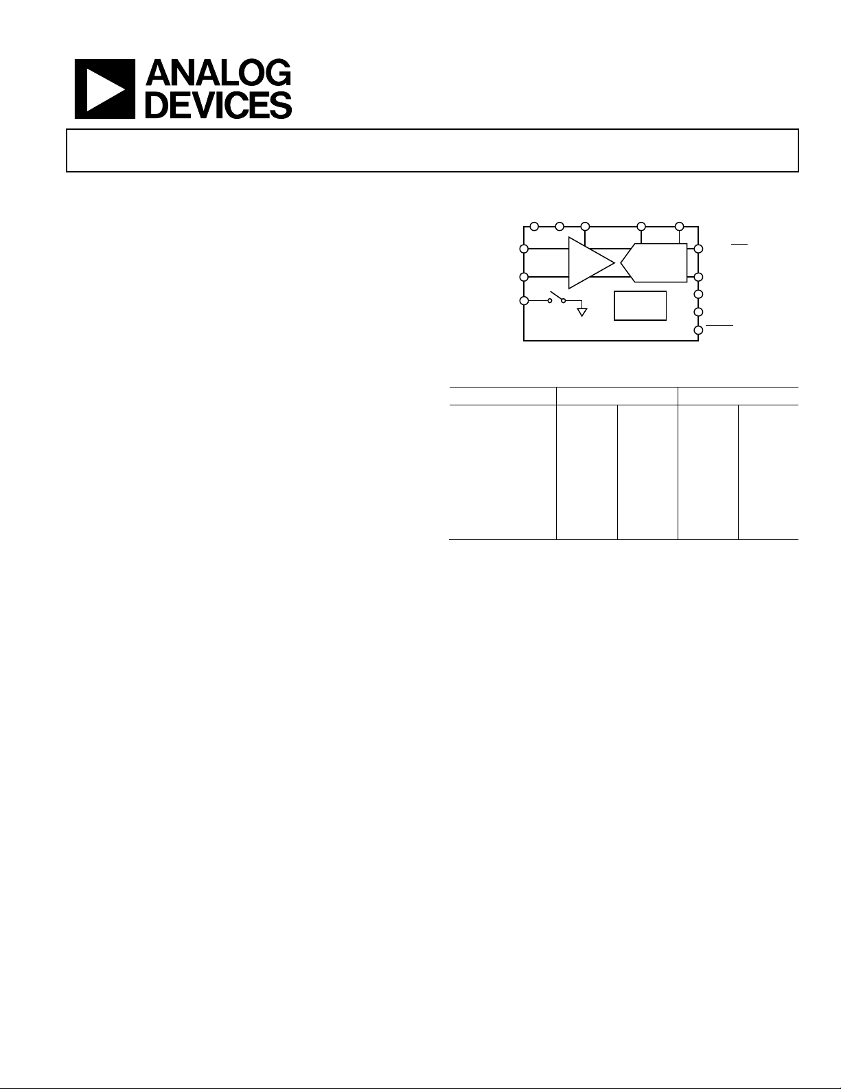
FUNCTIONAL BLOCK DIAGRAM
V
GND
DD
AIN(+)
AIN(–) SCLK
BPDSW
AD7781
G = 1
OR 128
Table 1.
Parameter Gain = 128 Gain = 1
Output Data Rate 10 Hz 16.7 Hz 10 Hz 16.7 Hz
RMS Noise
C Grade 44 nV 65 nV 2.4 V 2.7 V
B Grade 55 nV 90 nV 2.4 V 2.7 V
P-P Resolution
C Grade 17.6 17.1 18.8 18.7
B Grade 17.3 16.6 18.8 18.7
Settling Time 300 ms 120 ms 300 ms 120 ms
REFIN(+)GAIN REFIN(–)
20-BIT Σ-Δ
INTERNAL
CLOCK
Figure 1.
ADC
DOUT/RDY
DV
DD
FILTER
PDRST
08162-001
GENERAL DESCRIPTION
The AD7781 is a complete, low power front-end solution for
bridge sensor products, including weigh scales, strain gages,
and pressure sensors. It contains a precision, low power, 20-bit
sigma-delta (Σ-) ADC, an on-chip, low noise programmable
gain amplifier (PGA), and an on-chip oscillator.
Consuming only 330 µA, the AD7781 is particularly suitable for
portable or battery-operated products where very low power is
required. The AD7781 also has a power-down mode that allows
the user to switch off the power to the bridge sensor and power
down the AD7781 when not converting, thus increasing the
battery life of the product.
For ease of use, all the features of the AD7781 are controlled by
dedicated pins. Each time that a data read occurs, eight status bits
are appended to the 20-bit conversion. These status bits contain a
pattern sequence that can be used to confirm the validity of the
serial transfer.
Rev. 0
Information furnished by Analog Devices is believed to be accurate and reliable. However, no
responsibility is assumed by Analog Devices for its use, nor for any infringements of patents or other
rights of third parties that may result from its use. Specifications subject to change without notice. No
license is granted by implication or otherwise under any patent or patent rights of Analog Devices.
Trademarks and registered trademarks are the property of their respective owners.
The on-chip PGA has a gain of 1 or 128, supporting a full-scale
differential input of ±5 V or ±39 mV. The device has two filter
response options. The filter response at the 16.7 Hz update rate
provides superior dynamic performance. The settling time is
120 ms at this update rate. At the 10 Hz update rate, the filter
response provides better than −45 dB of stop-band attenuation.
In load cell applications, this stop-band rejection is useful to
reject low frequency mechanical vibrations of the load cell. The
settling time is 300 ms at this update rate. Simultaneous 50 Hz/
60 Hz rejection occurs at both the 10 Hz and 16.7 Hz update rates.
The AD7781 operates with a power supply from 2.7 V to 5.25 V.
It is available in a narrow body, 14-lead SOIC package and in a
16-lead TSSOP package.
One Technology Way, P.O. Box 9106, Norwood, MA 02062-9106, U.S.A.
Tel: 781.329.4700 www.analog.com
Fax: 781.461.3113 ©2009 Analog Devices, Inc. All rights reserved.

AD7781
http://www.BDTIC.com/ADI
TABLE OF CONTENTS
Features .............................................................................................. 1
Applications ....................................................................................... 1
Functional Block Diagram .............................................................. 1
General Description ......................................................................... 1
Revision History ............................................................................... 2
Specifications ..................................................................................... 3
Timing Characteristics ................................................................ 5
Absolute Maximum Ratings ............................................................ 6
Thermal Resistance ...................................................................... 6
ESD Caution .................................................................................. 6
Pin Configurations and Function Descriptions ........................... 7
Typical Performance Characteristics ............................................. 8
Output Noise and Resolution........................................................ 10
Theory of Operation ...................................................................... 11
Filter, Data Rate, and Settling Time ......................................... 11
Gain .............................................................................................. 11
Power-Down/Reset (
Analog Input Channel ............................................................... 12
Bipolar Configuration ................................................................ 12
Data Output Coding .................................................................. 12
Reference ..................................................................................... 12
Bridge Power-Down Switch ...................................................... 12
Digital Interface .......................................................................... 13
Applications Information .............................................................. 14
Weigh Scales ................................................................................ 14
AD7781 Performance in a Weigh Scale System ......................... 14
EMI Recommendations ............................................................. 14
Grounding and Layout .............................................................. 15
Outline Dimensions ....................................................................... 16
Ordering Guide .......................................................................... 16
PDRST
) ................................................... 12
REVISION HISTORY
5/09—Revision 0: Initial Version
Rev. 0 | Page 2 of 16

AD7781
http://www.BDTIC.com/ADI
SPECIFICATIONS
AVDD = 2.7 V to 5.25 V, V
Table 2.
Parameter Min Typ Max Unit Test Conditions/Comments
ADC CHANNEL
Output Update Rate (f
16.7 Hz FILTER = 0, settling time = 2/f
No Missing Codes
Resolution, Peak-to-Peak See Table 7 and Table 8
RMS Noise See Tab le 7 and Tabl e 8
Integral Nonlinearity ±6 ppm FSR
Offset Error ±6 µV Gain = 128 with FILTER = 1
±200 µV Gain = 1 with FILTER = 1
±1 µV Gain = 128 with FILTER = 0
±10 µV Gain = 1 with FILTER = 0
Offset Error Drift vs. Temperature ±10 nV/°C Gain = 128
±150 nV/°C Gain = 1 with FILTER = 1
±10 nV/°C Gain = 1 with FILTER = 0
Full-Scale Error ±0.25 % of FS
Gain Drift vs. Temperature ±2 ppm/°C
Power Supply Rejection 100 dB Gain = 128, FILTER = 1, AIN = 7.81 mV
120 dB Gain = 128, FILTER = 0, AIN = 7.81 mV
Normal Mode Rejection
50 Hz, 60 Hz 63 75 dB 50 Hz ± 1 Hz, 60 Hz ± 1 Hz, f
72 90 dB 50 Hz ± 1 Hz, 60 Hz ± 1 Hz, f
Common-Mode Rejection
DC 90 dB Gain = 1, AIN = 1 V
90 dB Gain = 128, AIN = 7.81 mV
50 Hz, 60 Hz 110 dB 50 Hz ± 1 Hz, 60 Hz ± 1 Hz
ANALOG INPUTS
Differential Input Voltage Range ±V
Absolute AIN Voltage Limits
GND + 450 mV AVDD − 1.1 V Gain = 128, FILTER = 0
GND + 1.1 AVDD − 1.1 V Gain = 128, FILTER = 1, AVDD ≤ 3.6 V
GND + 1.5 AVDD − 1.5 V Gain = 128, FILTER = 1, AVDD > 3.6 V
Average Input Current ±1 nA Gain = 1
±250 pA Gain = 128
Average Input Current Drift ±3 pA/°C
REFERENCE
External REFIN Voltage AVDD V REFIN = REFIN(+) − REFIN(−)
Reference Voltage Range
Absolute REFIN Voltage Limits
Average Reference Input Current 400 nA/V
Average Reference Input Current
Drift
Normal Mode Rejection Same as for analog inputs
Common-Mode Rejection 110 dB
BRIDGE POWER-DOWN SWITCH
(BPDSW)
RON 9 Ω
Allowable Current
= AVDD, DVDD = 2.7 V to 5.25 V, GND = 0 V, all specifications T
REF
) 10 Hz FILTER = 1, settling time = 3/f
ADC
2
2
20 Bits
/gain V
REF
MIN
to T
, unless otherwise noted.1
MAX
= REFIN(+) − REFIN(−),
V
REF
ADC
ADC
= 16.7 Hz
ADC
= 10 Hz
ADC
gain = 1 or 128
2
GND + 100 mV AV
2
0.5 AV
2
GND − 30 mV AV
− 100 mV V Gain = 1
DD
V
DD
+ 30 mV V
DD
±0.15 nA/V/°C
2
30 mA Continuous current
Controlled via the PDRST
pin
Rev. 0 | Page 3 of 16

AD7781
http://www.BDTIC.com/ADI
Parameter Min Typ Max Unit Test Conditions/Comments
INTERNAL CLOCK
Frequency 64 − 3% 64 + 3% kHz
Duty Cycle 50:50 %
LOGIC INPUTS
SCLK, FILTER, GAIN, PDRST
Input Low Voltage, V
0.8 V DVDD = 5 V
Input High Voltage, V
2.4 V DVDD = 5 V
SCLK (Schmitt-Triggered Input)
Hysteresis
2
100 mV DV
140 mV DVDD = 5 V
Input Currents ±2 µA VIN = DVDD or GND
Input Capacitance 10 pF All digital inputs
LOGIC OUTPUT (DOUT/RDY)
Output High Voltage, V
4 V DVDD = 5 V, I
Output Low Voltage, V
0.4 V DVDD = 5 V, I
Floating-State Leakage Current ±2 µA
Floating-State Output Capacitance 10 pF
Data Output Coding Offset binary
POWER REQUIREMENTS
Power Supply Voltage
AVDD to GND 2.7 5.25 V
DVDD to GND 2.7 5.25 V
Power Supply Currents
IDD Current
Gain = 1 115 µA AVDD = 3 V
130 160 µA AVDD = 5 V
Gain = 128 (B Grade) 300 µA AVDD = 3 V
350 400 µA AVDD = 5 V
Gain = 128 (C Grade) 330 µA AVDD = 3 V
420 500 µA AVDD = 5 V
IDD (Power-Down/Reset Mode) 10 µA
1
Temperature range is −40°C to +105°C.
2
This specification is not production tested but is supported by characterization data at initial product release.
3
Digital inputs are equal to DVDD or GND.
2
0.4 V DVDD = 3 V
INL
1.8 V DVDD = 3 V
INH
2
DV
OH
2
0.4 V DV
OL
3
− 0.6 V DVDD = 3 V, I
DD
= 3 V
DD
= 3 V, I
DD
SOURCE
SOURCE
= 100 µA
SINK
= 1.6 mA
SINK
= 100 µA
= 200 µA
Rev. 0 | Page 4 of 16
AD7781
http://www.BDTIC.com/ADI
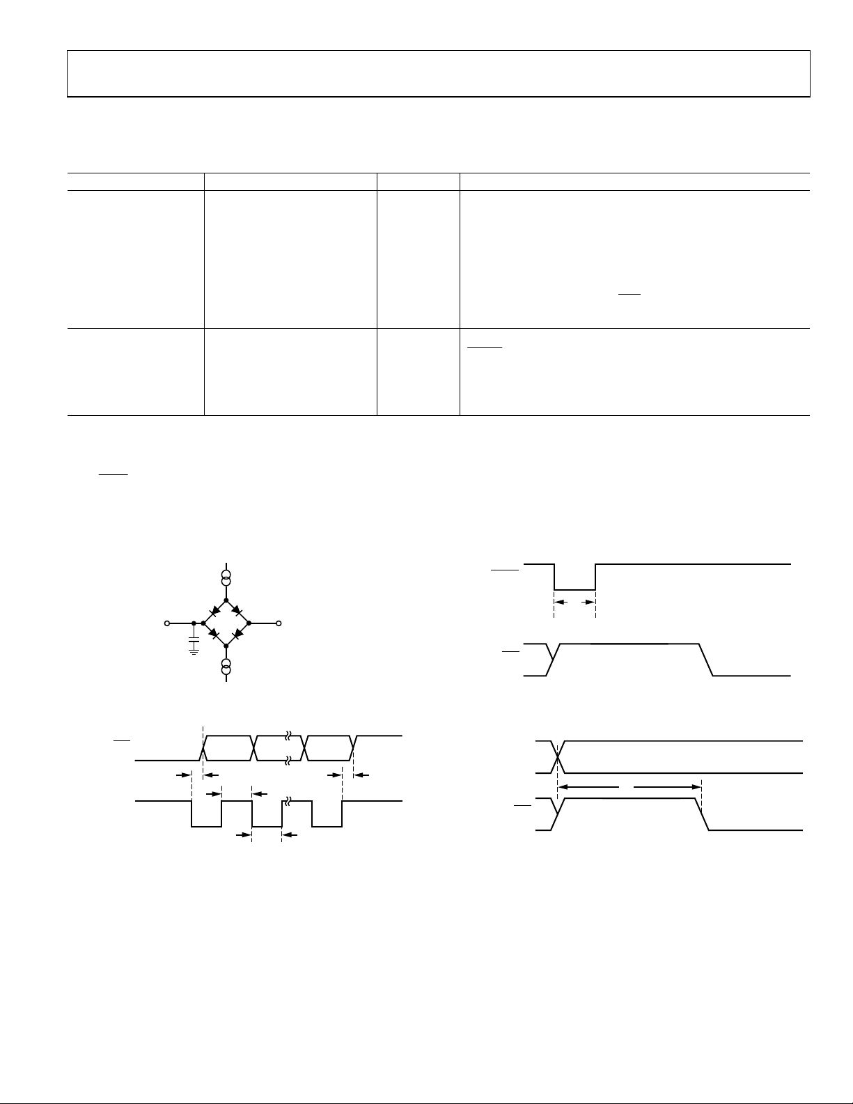
TIMING CHARACTERISTICS
AVDD = 2.7 V to 5.25 V, DVDD = 2.7 V to 5.25 V, GND = 0 V, Input Logic 0 = 0 V, Input Logic 1 = DVDD, unless otherwise noted.
Table 3.
Parameter
Read
1
2
Limit at T
MIN
, T
Unit Test Conditions/Comments
MAX
t1 100 ns min SCLK high pulse width
t2 100 ns min SCLK low pulse width
3
t
3
0 ns min SCLK active edge to data valid delay
4
60 ns max DVDD = 4.75 V to 5.25 V
80 ns max DVDD = 2.7 V to 3.6 V
t4 10 ns min
SCLK inactive edge to DOUT/RDY
high
130 ns max
Reset
t5 100 ns min
5
t
6
FILTER/GAIN change to data valid delay
low pulse width
PDRST
120 ms typ Update rate = 16.7 Hz
300 ms typ Update rate = 10 Hz
1
Sample tested during initial release to ensure compliance. All input signals are specified with tR = tF = 5 ns (10% to 90% of DVDD) and timed from a voltage level of 1.6 V.
2
See Figure 3.
3
The values of t3 are measured using the load circuit of Figure 2 and are defined as the time required for the output to cross the VOL or VOH limits.
4
SCLK active edge is falling edge of SCLK.
5
PDRST
The
high to data valid delay is typically 1 ms longer than t6 because the internal oscillator requires time to power up and settle.
Circuit and Timing Diagrams
DOUT/RDY
(OUTPUT)
SCLK
(INPUT)
I
(1.6mA WITH DVDD = 5V,
TO
OUTPUT
PIN
50pF
SINK
100µA WIT H DV
I
SOURCE
100µA WIT H DV
= 3V)
DD
1.6V
(200µA WIT H DVDD = 5V,
= 3V)
DD
Figure 2. Load Circuit for Timing Characterization
MSB LSB
t
3
t
1
t
2
t
Figure 3. Read Cycle Timing Diagram
PDRST
(INPUT)
t
5
DOUT/RDY
08162-002
(OUTPUT)
08162-004
Figure 4. Resetting the AD7781
GAIN OR FILTER
(INPUT)
4
DOUT/RDY
(OUTPUT)
08162-003
t
6
08162-005
Figure 5. Changing Gain or Filter Option
Rev. 0 | Page 5 of 16

AD7781
http://www.BDTIC.com/ADI
ABSOLUTE MAXIMUM RATINGS
TA = 25°C, unless otherwise noted.
Table 4.
Parameter Rating
AVDD to GND −0.3 V to +7 V
DVDD to GND −0.3 V to +7 V
Analog Input Voltage to GND −0.3 V to AVDD + 0.3 V
Reference Input Voltage to GND −0.3 V to AVDD + 0.3 V
Digital Input Voltage to GND −0.3 V to DVDD + 0.3 V
Digital Output Voltage to GND −0.3 V to DVDD + 0.3 V
AIN/Digital Input Current 10 mA
Operating Temperature Range −40°C to +105°C
Storage Temperature Range −65°C to +150°C
Maximum Junction Temperature 150°C
Lead Temperature, Soldering Reflow 260°C
Stresses above those listed under Absolute Maximum Ratings
may cause permanent damage to the device. This is a stress
rating only; functional operation of the device at these or any
other conditions above those indicated in the operational
section of this specification is not implied. Exposure to absolute
maximum rating conditions for extended periods may affect
device reliability.
THERMAL RESISTANCE
θJA is specified for the worst-case conditions, that is, a device
soldered in a circuit board for surface-mount packages.
Table 5.
Package Type θJA θ
14-Lead SOIC 104.5 42.9 °C/W
16-Lead TSSOP 150.4 27.6 °C/W
Unit
JC
ESD CAUTION
Rev. 0 | Page 6 of 16

AD7781
http://www.BDTIC.com/ADI
PIN CONFIGURATIONS AND FUNCTION DESCRIPTIONS
16
15
14
13
12
11
10
9
NC
FILTER
PDRST
DV
DD
AV
DD
GND
BPDSW
REFIN(–)
08162-007
1
SCLK
DOUT/RDY 2
NC 3
AD7781
TOP VIEW
4
GAIN
AIN(+) 5 GND10
AIN(–) 6 BPDSW9
REFIN(+)
(Not to Scale)
7
NC = NO CONNECT
14
12
11
8
FILTER
PDRST13
DV
DD
AV
DD
REFIN(–)
1
NC
2
SCLK
NC
GAIN
AIN(+)
AIN(–)
3
AD7781
4
TOP VIEW
(Not to Scale)
5
6
7
8
NC = NO CO NNECT
DOUT/RDY
8162-006
REFIN(+)
Figure 6. SOIC Pin Configuration Figure 7. TSSOP Pin Configuration
Table 6. Pin Function Descriptions
Pin No.
SOIC TSSOP Mnemonic Description
1 2 SCLK
Serial Clock Input. This serial clock input is for data transfers from the ADC. The SCLK pin has a Schmitttriggered input. The serial clock can be active only when transferring data from the AD7781. The data
from the AD7781 can be read as a continuous 32-bit word. Alternatively, SCLK can be noncontinuous
during the data transfer, with the information being transmitted from the ADC in smaller data batches.
2 3
DOUT/RDY
Serial Data Output/Data Ready Output. DOUT/RDY serves a dual purpose: as a data ready pin, going low
to indicate the completion of a conversion, and as a serial data output pin to access the data register of
the ADC. Eight status bits accompany each data read (see ). The DOUT/Figure 22 RDY falling edge can be
used as an interrupt to a processor, indicating that new data is available. If the data is not read after the
conversion, the pin goes high before the next update occurs. The serial interface is reset each time that a
conversion is available. Therefore, the user must ensure that any conversions being transmitted are
completed before the next conversion is available.
3 1, 4, 16 NC No Connect. This pin can be left floating.
4 5 GAIN Gain Select Pin. When GAIN is low, the gain is set to 128. When GAIN is high, the gain is set to 1.
5 6 AIN(+) Analog Input. AIN(+) is the positive terminal of the differential analog input pair, AIN(+)/AIN(−).
6 7 AIN(−) Analog Input. AIN(−) is the negative terminal of the differential analog input pair, AIN(+)/AIN(−).
7 8 REFIN(+)
Positive Reference Input. An external reference can be applied between REFIN(+) and REFIN(−). The nomi-
nal reference voltage (REFIN(+) − REFIN(−)) is 5 V, but the part can function with a reference of 0.5 V to AVDD.
8 9 REFIN(−) Negative Reference Input.
9 10 BPDSW
Bridge Power-Down Switch to GND. When PDRST
When PDRST
is low, the switch is opened.
is high, the bridge power-down switch is closed.
10 11 GND Ground Reference Point.
11 12 AVDD Supply Voltage, 2.7 V to 5.25 V.
12 13 DVDD
13 14
PDRST
Digital Interface Supply Voltage. The logic levels for the serial interface pins and the digital control pins
are related to this supply, which is between 2.7 V and 5.25 V. The DV
voltage on AV
Power-Down/Reset. When this pin is low, the ADC is placed in power-down mode, and the low-side power
; therefore, AVDD can equal 5 V with DVDD at 3 V or vice versa.
DD
switch is opened. All the logic on the chip is reset, and the DOUT/RDY
voltage is independent of the
DD
pin is tristated. When PDRST is high,
the ADC is taken out of power-down mode. The on-chip clock powers up and settles, and the ADC continuously converts. In addition, the low-side power switch is closed. The internal clock requires approximately
1 ms to power up.
14 15 FILTER
Filter Select Pin. When FILTER is low, the fast settling filter is selected. The update rate is set to 16.7 Hz,
which gives a filter settling time of 120 ms. When FILTER is high, the high rejection filter is selected. The
update rate is set to 10 Hz, which gives a filter settling time of 300 ms. With this filter, the stop-band
(higher than f
) attenuation is better than −45 dB.
ADC
Rev. 0 | Page 7 of 16

AD7781
http://www.BDTIC.com/ADI
TYPICAL PERFORMANCE CHARACTERISTICS
524,294
524,293
524,292
524,291
524,290
CODE
524,289
524,288
524,287
600
400
OCCURRENCE
200
524,286
0 200 400 600 800 1000
Figure 8. C Grade Noise (V
500
400
300
200
OCCURRENCE
100
0
524,286 524, 288 524,290 524,292 524,294
SAMPLE
= AVDD, Update Rate = 16.7 Hz, Gain = 128)
REF
CODE
Figure 9. C Grade Noise Distribution Histogram
= AVDD, Update Rate = 16.7 Hz, Gain = 128)
(V
REF
524,281
0
524,275 524,277 524, 279 MORE
08162-008
CODE
08162-011
Figure 11. C Grade Noise Distribution Histogram
= AVDD, Update Rate = 10 Hz, Gain = 128)
(V
REF
524,289
524,288
CODE
524,287
524,286
0 200 400 600 800 1000
08162-009
Figure 12. Noise (V
505
REF
SAMPLE
= AVDD, Update Rate = 16.7 Hz, Gain = 1)
08162-012
524,280
524,279
524,278
CODE
524,277
524,276
524,275
524,274
0 200 400 600 800 1000
Figure 10. C Grade Noise (V
SAMPLE
= AVDD, Update Rate = 10 Hz, Gain = 128)
REF
08162-010
Rev. 0 | Page 8 of 16
500
OCCURRENCE
495
524,287 524,288
CODE
Figure 13. Noise Distribution Histogram
= AVDD, Update Rate = 16.7 Hz, Gain = 1)
(V
REF
162-01308

AD7781
http://www.BDTIC.com/ADI
524,276
524,275
2.0
1.5
1.0
0.5
CODE
524,274
524,273
0 200 400 600 800 1000
Figure 14. Noise (V
800
600
400
OCCURRENCE
200
0
REF
524,274 524,275
SAMPLE
= AVDD, Update Rate = 10 Hz, Gain = 1)
CODE
Figure 15. Noise Distribution Histogram
= AVDD, Update Rate = 10 Hz, Gain = 1)
(V
REF
0
INL (ppm FS)
–0.5
–1.0
–1.5
–2.0
–6 –4 –2 0 2 4 6
08162-014
Figure 17. Integral Nonlinearity (V
10
8
6
4
2
0
–2
OFFSET (µV)
–4
–6
–8
–10
162-015
08
–60 –40 –20 0 20 40 60 80 100 120
V
(V)
IN
REF
TEMPERATURE (° C)
= AVDD, Gain = 1)
08162-017
08162-018
Figure 18. Offset vs. Temperature (Gain = 128)
3.0
2.5
2.0
1.5
1.0
0.5
0
INL (ppm FS)
–0.5
–1.0
–1.5
–2.0
–2.5
–0.04 –0.03 –0.02 –0.01 0 0.01 0.02 0. 03 0.04
Figure 16. Integral Nonlinearity (V
(V)
V
IN
REF
= AVDD, Gain = 128)
08162-016
Rev. 0 | Page 9 of 16
150
100
50
0
–50
GAIN ERROR (ppm)
–100
–150
–200
–60 –40 –20 0 2 0 40 60 80 100 120
TEMPERATURE (°C)
Figure 19. Gain Error vs. Temperature (Gain = 128)
08162-019

AD7781
http://www.BDTIC.com/ADI
OUTPUT NOISE AND RESOLUTION
Tabl e 7 and Tab l e 8 show the rms noise of the AD7781 for the two output data rates and gain settings when using a 3 V and a 5 V reference.
These numbers are typical and are generated with a differential input voltage of 0 V. The peak-to-peak (p-p) resolution is also listed. The
p-p resolution represents the resolution for which there is no code flicker. These numbers are typical.
Table 7. RMS Noise and Peak-to-Peak Resolution When AV
Parameter Gain = 128 Gain = 1
Update Rate 10 Hz 16.7 Hz 10 Hz 16.7 Hz
RMS Noise
C Grade 44 nV 65 nV 2.4 V 2.7 V
B Grade 55 nV 90 nV 2.4 V 2.7 V
P-P Resolution
C Grade 17.6 17.1 18.8 18.7
B Grade 17.3 16.6 18.8 18.7
= 3 V and V
DD
REF
= 3 V
Table 8. RMS Noise and Peak-to-Peak Resolution When AV
Parameter Gain = 128 Gain = 1
Update Rate 10 Hz 16.7 Hz 10 Hz 16.7 Hz
RMS Noise
C Grade 49 nV 69 nV 3.0 V 2.7 V
B Grade 60 nV 90 nV 3.0 V 2.7 V
P-P Resolution
C Grade 18.2 17.7 19.3 19.4
B Grade 17.9 17.3 19.3 19.4
= 5 V and V
DD
REF
= 5 V
Rev. 0 | Page 10 of 16

AD7781
http://www.BDTIC.com/ADI
THEORY OF OPERATION
The AD7781 is a low power ADC that incorporates a precision,
20-bit, Σ-∆ modulator; a PGA; and an on-chip digital filter
intended for measuring wide dynamic range, low frequency
signals. The part provides a complete front-end solution for
bridge sensor applications such as weigh scales and pressure
sensors.
The device has an internal clock and one buffered differential
input. It offers a choice of two update rates (10 Hz or 16.7 Hz)
and two gain settings (1 or 128). These functions are controlled
using dedicated pins, which makes the interface easy to configure.
A 2-wire interface simplifies data retrieval from the AD7781.
FILTER, DATA RATE, AND SETTLING TIME
The AD7781 has two filter options. When the FILTER pin is
low, the 16.7 Hz filter is selected; when the FILTER pin is high,
the 10 Hz filter is selected. When the polarity of the FILTER pin
is changed, the AD7781 modulator and filter are reset immediately. DOUT/
using the selected filter response. The first conversion requires
the total settling time of the filter. Subsequent conversions
occur at the selected update rate. The settling time of the 10 Hz
filter is 300 ms (three conversion cycles), and the settling time
of the 16.7 Hz filter is 120 ms (two conversion cycles).
When a step change occurs on the analog input, the AD7781
requires several conversion cycles to generate a valid conversion.
If the step change occurs synchronous to the conversion period, the
settling time of the AD7781 must be allowed to generate a valid
conversion. If the step change occurs asynchronous to the end
of a conversion, an extra conversion must be allowed to generate
a valid conversion. The data register is updated with all the conversions, but, for an accurate result, the user must allow for the
required time.
Figure 20 and Figure 21 show the filter response for each filter.
The 10 Hz filter provides more than −45 dB of rejection in the
stop band. The only external filtering required on the analog
inputs is a simple R-C filter to provide rejection at multiples of
the master clock. A 1 k resistor in series with each analog input,
a 0.01 F capacitor from each input to GND, and a 0.1 F
capacitor from AIN(+) to AIN(−) are recommended.
When the filter is changed, DOUT/
high until the appropriate settling time for that filter elapses
(see ). Therefore, the user should complete any read
Figure 5
operations before changing the filter. Otherwise, 1s are read
back from the AD7781 because the DOUT/
following the filter change.
RDY
is set high, and the ADC begins conversions
RDY
goes high and remains
RDY
pin is set high
0
–20
–40
–60
FILTER GAIN (dB)
–80
–100
–120
012010080604020
Figure 20. Filter Profile with Update Rate = 16.7 Hz (FILTER = 0)
INPUT SIGNAL FREQUENCY (Hz)
08162-020
0
–20
–40
–60
FILTER GAIN (dB)
–80
–100
–120
0 12010080604020
Figure 21. Filter Profile with Update Rate = 10 Hz (FILTER = 1)
INPUT SIG NAL FREQUENCY ( Hz)
08162-021
GAIN
The AD7781 has two gain options: gain = 1 and gain = 128.
When the GAIN pin is low, the gain is set to 128; when the
GAIN pin is high, the gain is set to 1. The acceptable analog
input range is ±V
is ±5 V when GAIN is high and ±39 mV when GAIN is low.
When the polarity of the GAIN pin is changed, the AD7781 modulator and filter are reset immediately. DOUT/
the ADC begins conversions. DOUT/
the appropriate settling time for the filter elapses (see ).
Therefore, the user should complete any read operations before
changing the gain. Otherwise, 1s are read back from the AD7781
because the DOUT/
The total settling time of the selected filter is required to generate
the first conversion after the gain change; subsequent conversions
occur at the selected update rate.
/gain. Thus, with V
REF
= 5 V, the input range
REF
RDY
RDY
remains high until
RDY
pin is set high following the gain change.
is set high, and
Figure 5
Rev. 0 | Page 11 of 16

AD7781
http://www.BDTIC.com/ADI
POWER-DOWN/RESET (PDRST)
PDRST
The
When
pin functions as a power-down pin and a reset pin.
PDRST
is taken low, the AD7781 is powered down. The
entire ADC is powered down (including the on-chip clock), the
low-side power switch is opened, and the DOUT/
RDY
pin is
tristated. The circuitry and serial interface are also reset, which
resets the logic, the digital filter, and the analog modulator.
PDRST
must be held low for 100 ns minimum to initiate the
reset function (see ). Figure 4
PDRST
When
is taken high, the AD7781 is taken out of powerdown mode. When the on-chip clock has powered up (1 ms,
typically), the modulator begins sampling the analog input.
The low-side power switch is closed, and the DOUT/
RDY
pin
becomes active.
A reset is automatically performed on power-up.
ANALOG INPUT CHANNEL
The AD7781 has one differential analog input channel. The
input channel feeds into a high impedance input stage of the
amplifier. Therefore, the input can tolerate significant source
impedances and is tailored for direct connection to external
resistive-type sensors such as strain gages.
The absolute input voltage range is restricted to a range between
GND + 450 mV and AV
− 1.1 V. Care must be taken in setting
DD
up the common-mode voltage to avoid exceeding these limits.
Otherwise, there is degradation in linearity and noise performance.
The low noise in-amp means that signals of small amplitude can
be amplified within the AD7781, which still maintains excellent
noise performance. The amplifier can be configured to have a gain
of 128 or 1, using the GAIN pin. The analog input range is equal
to ±V
/gain. The common-mode voltage (AIN(+) + AIN(−))/2
REF
must be ≥0.5 V.
BIPOLAR CONFIGURATION
The AD7781 accepts a bipolar input range. A bipolar input range
does not imply that the part can tolerate negative voltages with
respect to system GND. Signals on the AIN(+) input are referenced to the voltage on the AIN(−) input. For example, if AIN(−)
is 2.5 V, the analog input range on the AIN(+) input is 2.46 V to
2.54 V for a gain of 128.
DATA OUTPUT CODING
The AD7781 uses offset binary coding. Thus, a negative fullscale voltage results in a code of 000...000, a zero differential
input voltage results in a code of 100...000, and a positive fullscale input voltage results in a code of 111...111.
The output code for any analog input voltage can be represented as
Code = 2
N − 1
× [(AIN × Gain/V
REF
) + 1]
where:
AIN is the analog input voltage.
Gain is 1 or 128.
N = 20.
REFERENCE
The AD7781 has a fully differential input capability for the channel.
The common-mode range for these differential inputs is GND to
. The reference input is unbuffered; therefore, excessive R-C
AV
DD
source impedances introduce gain errors. The reference voltage of
REFIN (REFIN(+) − REFIN(−)) is AV
is functional with reference voltages of 0.5 V to AV
nominal, but the AD7781
DD
. In applica-
DD
tions where the excitation (voltage or current) for the transducer
on the analog input also drives the reference voltage for the part,
the effect of the low frequency noise in the excitation source is
removed because the application is ratiometric. If the AD7781
is used in a nonratiometric application, a low noise reference
should be used.
Recommended 2.5 V reference voltage sources for the AD7781
include the ADR381 and ADR391, which are low noise, low power
references. These references have low output impedances and
are, therefore, tolerant to decoupling capacitors on REFIN(+)
without introducing gain errors in the system. Deriving the
reference input voltage across an external resistor means that
the reference input sees a significant external source impedance.
External decoupling on the REFIN pins is not recommended in
this type of circuit configuration.
BRIDGE POWER-DOWN SWITCH
The bridge power-down switch (BPDSW) is useful in batterypowered applications where the optimization of system power
consumption is essential. A 350 load cell typically consumes
15 mA when excited with a 5 V power supply. To minimize
current consumption, the load cell is disconnected when it is
not being used. The bridge power-down switch can be included
in series with the load cell. When
down switch is closed, and the load cell measures the strain. When
is low, the bridge power-down switch is opened so no
PDRST
current flows through the load cell. Therefore, the current
consumption of the system is minimized. The bridge powerdown switch has an on resistance of 9 maximum. The switch
is capable of withstanding 30 mA of continuous current.
is high, the bridge power-
PDRST
Rev. 0 | Page 12 of 16

AD7781
http://www.BDTIC.com/ADI
DIGITAL INTERFACE
The serial interface of the AD7781 consists of two signals: SCLK
and DOUT/
and data transfers occur with respect to the SCLK signal. The
DOUT/
pin and as a data output pin. DOUT/
data-word is available in the output register. A 32-bit word is
placed on the DOUT/
applied. This word consists of a 20-bit conversion result followed
by four 0s to generate a 24-bit word. Following this, status bits
are output. shows the status bits, and describes
the status bits and their functions.
DOUT/
If the conversion is not read, DOUT/
data register update to indicate when not to read from the device.
This ensures that a read operation is not attempted while the register is being updated. Each conversion can be read only once. The
data register is updated for every conversion.
RDY
. SCLK is the serial clock input for the device,
RDY
pin is dual purpose: it functions as a data ready
RDY
goes low when a new
RDY
pin when sufficient SCLK pulses are
Figure 22 Tabl e 9
FILTER ERRRDY ID1 ID0 GAIN PAT1 PAT0
Figure 22. Status Bits
RDY
is reset high when the conversion has been read.
RDY
goes high prior to the
08162-022
When a conversion is complete, the serial interface is reset, and
the new conversion is placed in the data register. Therefore, the
user must ensure that the complete word is read before the next
conversion is complete.
PDRST
When
PDRST
is low, the DOUT/
is taken high, the internal clock requires approximately
RDY
pin is tristated. When
1 ms to power up. Following power-up, the ADC continuously
converts. The first conversion requires the total settling time
(see ). DOUT/Figure 4
RDY
goes high when
PDRST
is taken
high and returns low only when a conversion is available. The
ADC then converts continuously, and subsequent conversions
are available at the selected update rate. shows the
Figure 3
timing for a read operation from the AD7781.
When the filter response is changed (using the FILTER pin) or
the gain is changed (using the GAIN pin), the modulator and
filter are reset immediately (see Figure 5). DOUT/
RDY
is set
high. The ADC then begins conversions using the selected filter
response/gain setting. DOUT/
RDY
remains high until the appropriate settling time for that filter has elapsed. Therefore, the user
should complete any read operations before changing the gain or
update rate. Otherwise, 1s are read back from the AD7781 because
the DOUT/
RDY
pin is set high following the gain/filter change.
Table 9. Status Bit Functions
Bit Name Description
RDY
0: a conversion is available.
FILTER Filter bit.
1: 10 Hz filter is selected.
0: 16.7 Hz filter is selected.
ERR Error bit.
1: an error occurred during conversion. (An error occurs when the analog input is out of range.)
ID1, ID0 ID bits.
0 0 Indicates the ID number for the AD7781.
GAIN Gain bit.
1: gain = 1.
0: gain = 128.
PAT1, PAT0 Status pattern bits. When the user reads data from the AD7781, a pattern check can be performed.
0 1 Indicates that the serial transfer from the ADC was performed correctly (default).
0 0 Indicates that the serial transfer from the ADC was not performed correctly.
1 x Indicates that the serial transfer from the ADC was not performed correctly.
Ready bit.
ID1 ID0 Function
PAT1 PAT0 Func tion
Rev. 0 | Page 13 of 16

AD7781
V
http://www.BDTIC.com/ADI
APPLICATIONS INFORMATION
The AD7781 provides a low cost, high resolution analog-todigital function. Because the analog-to-digital function is
provided by a Σ- architecture, the part is more immune to
noisy environments, making it ideal for use in sensor measurement and industrial and process control applications.
(the conversion result from the ADC when the maximum load
is applied to the load cell) must be determined. Subsequent
conversions from the AD7781 are then corrected, using the
offset and gain coefficients that were calculated from these
calibrations.
WEIGH SCALES
Figure 23 shows the AD7781 being used in a weigh scale
application. The load cell is arranged in a bridge network and
gives a differential output voltage between its OUT+ and OUT−
terminals. Assuming a 5 V excitation voltage, the full-scale
output range from the transducer is 10 mV when the sensitivity
is 2 mV/V. The excitation voltage for the bridge can be used to
directly provide the reference for the ADC because the reference input range includes the supply voltage.
A second advantage of using the AD7781 in transducer-based
applications is that the bridge power-down switch (BPDSW)
can be fully utilized in low power applications. The bridge powerdown switch is connected in series with the low side of the bridge.
In normal operation, the switch is closed and measurements
can be taken. In applications where power is of concern, the
AD7781 can be placed in power-down mode, significantly
reducing the power consumed in the application. In addition,
the bridge power-down switch is opened while in power-down
mode, thus avoiding unnecessary power consumption by the
front-end transducer. When the part is taken out of power-down
mode and the bridge power-down switch is closed, the user should
ensure that the front-end circuitry is fully settled before attempting
to read from the AD7781.
The load cell has an offset, or tare, associated with it. This tare is
the main component of the system offset (load cell + ADC) and
is similar in magnitude to the full-scale signal from the load cell.
For this reason, calibrating the offset and gain of the AD7781
alone is not sufficient for optimum accuracy; a system calibration
that calibrates the offset and gain of the ADC, plus the load cell,
is required. A microprocessor can be used to perform the calibrations. The offset error (the conversion result from the AD7781
when no load is applied to the load cell) and the full-scale error
DD
AD7781 PERFORMANCE IN A WEIGH SCALE SYSTEM
If the load cell has a sensitivity of 2 mV/V and a 5 V excitation
voltage is used, the full-scale signal from the load cell is 10 mV.
When the AD7781 (C grade) operates with a 10 Hz output data
rate and the gain is set to 128, the device has a p-p resolution of
18.2 bits when the reference is equal to 5 V. Postprocessing the
data from the AD7781 using a microprocessor increases the p-p
resolution. For example, an average by 4 in the microprocessor
increases the accuracy by 2 bits. The noise-free counts value is
equal to
Noise-Free Counts = (2
Effective Bits
) × (FSLC/FS
ADC
)
where:
Effective Bits = 18.2 bits (AD7781) + 2 bits (due to postprocessing
in the microprocessor).
FS
is the full-scale signal from the load cell (10 mV).
LC
FS
is the full-scale input range when gain = 128 and
ADC
V
= 5 V (78 mV).
REF
The noise-free counts is equal to
18.2 + 2
(2
) × (10 mV/78 mV) = 154,422
This example shows that with a 5 V supply, 154,422 noise-free
counts can be achieved with the AD7781.
EMI RECOMMENDATIONS
For simplicity, the EMI filters are not included in Figure 23.
However, an R-C antialiasing filter should be included on each
analog input. This filter is needed because the on-chip digital
filter does not provide any rejection around the master clock or
multiples of the master clock. Suitable values are a 1 kΩ resistor
in series with each analog input, a 0.1 F capacitor from AIN(+)
to AIN(−), and 0.01 F capacitors from AIN(+)/AIN(−) to GND.
IN+
OUT–
IN–
G = 1
OR 128
GND
REFIN(+)
AIN(+)
OUT+
AIN(–)
REFIN(–)
BPDSW
Figure 23. Weigh Scales Using the AD7781
Rev. 0 | Page 14 of 16
20-BIT Σ-Δ
INTERNAL
CLOCK
AD7781
AV
ADC
DD
DOUT/RDY
SCLK
DV
DD
FILTER
PDRST
GAIN
8162-023

AD7781
http://www.BDTIC.com/ADI
GROUNDING AND LAYOUT
Because the analog input and reference input of the ADC are
differential, most of the voltages in the analog modulator are
common-mode voltages. The excellent common-mode rejecttion of the part removes common-mode noise on these inputs.
The digital filter provides rejection of broadband noise on the
power supply, except at integer multiples of the modulator
sampling frequency. The digital filter also removes noise from
the analog and reference inputs, provided that these noise sources
do not saturate the analog modulator. As a result, the AD7781
is more immune to noise interference than conventional high
resolution converters. However, because the resolution of the
AD7781 is so high and the noise levels from the AD7781 are so
low, care must be taken with regard to grounding and layout.
The printed circuit board (PCB) that houses the AD7781 should
be designed so that the analog and digital sections are separated
and confined to certain areas of the board. A minimum etch
technique is generally best for ground planes because it gives
the best shielding.
It is recommended that the GND pin of the AD7781 be tied
to the AGND plane of the system. In any layout, pay attention
to the flow of currents in the system and ensure that the return
paths for all currents are as close as possible to the paths that the
currents took to reach their destinations. Avoid forcing digital
currents to flow through the AGND sections of the layout.
The ground plane of the AD7781 should be allowed to run under
the AD7781 to prevent noise coupling. The power supply lines
to the AD7781 should use as wide a trace as possible to provide
low impedance paths and reduce the effects of glitches on the
power supply line. Fast switching signals such as clocks should
be shielded with digital ground to avoid radiating noise to other
sections of the board, and clock signals should never be run near
the analog inputs. Avoid crossover of digital and analog signals.
Traces on opposite sides of the board should run at right angles
to each other. This reduces the effects of feedthrough through
the board. A microstrip technique is by far the best, but it is not
always possible with a double-sided board. In this technique,
the component side of the board is dedicated to ground planes,
and the signals are placed on the solder side.
Good decoupling is important when using high resolution ADCs.
AV
should be decoupled with 10 µF tantalum capacitors in
DD
parallel with 0.1 µF capacitors to GND. DV
with 10 µF tantalum capacitors in parallel with 0.1 µF capacitors to GND, with the system’s AGND to DGND connection
being close to the AD7781. To achieve the best results from
these decoupling components, place them as close as possible
to the device, ideally right up against the device. All logic chips
should be decoupled with 0.1 µF ceramic capacitors to DGND.
should be decoupled
DD
Rev. 0 | Page 15 of 16

AD7781
http://www.BDTIC.com/ADI
OUTLINE DIMENSIONS
0.25 (0.0098)
0.10 (0.0039)
COPLANARIT Y
8.75 (0.3445)
8.55 (0.3366)
4.00 (0.1575)
3.80 (0.1496)
0.10
14
1
1.27 (0.0500)
BSC
0.51 (0.0201)
0.31 (0.0122)
CONTROLL ING DIMENSIONS ARE IN MILLIMETERS; INCH DI MENSIONS
(IN PARENTHESES) ARE ROUNDED-O FF MIL LIMETE R EQUIVALENTS FOR
REFERENCE ON LY AND ARE NOT APPROPRI ATE FOR USE IN DESIGN.
COMPLIANT TO JEDEC STANDARDS MS-012-AB
8
6.20 (0.2441)
5.80 (0.2283)
7
1.75 (0.0689)
1.35 (0.0531)
SEATING
PLANE
8°
0°
0.25 (0.0098)
0.17 (0.0067)
Figure 24. 14-Lead Standard Small Outline Package [SOIC_N]
Narrow Body
(R-14)
Dimensions shown in millimeters and (inches)
5.10
5.00
4.90
0.15
0.05
4.50
4.40
4.30
PIN 1
16
0.65
BSC
COPLANARITY
COMPLIANT TO JEDEC STANDARDS MO-153-AB
0.10
0.30
0.19
9
BSC
81
1.20
MAX
SEATING
PLANE
6.40
0.20
0.09
8°
0°
Figure 25. 16-Lead Thin Shrink Small Outline Package [TSSOP]
(RU-16)
Dimensions shown in millimeters
0.50 (0.0197)
0.25 (0.0098)
1.27 (0.0500)
0.40 (0.0157)
0.75
0.60
0.45
45°
-A
060606
ORDERING GUIDE
Model Temperature Range Package Description Package Option
AD7781BRZ
AD7781BRZ-REEL
AD7781BRUZ
AD7781BRUZ-REEL
AD7781CRZ
AD7781CRZ-REEL
AD7781CRUZ
AD7781CRUZ-REEL
1
Z = RoHS Compliant Part.
©2009 Analog Devices, Inc. All rights reserved. Trademarks and
registered trademarks are the property of their respective owners.
D08162-0-5/09(0)
1
1
1
1
1
1
1
1
−40°C to +105°C 14-Lead SOIC_N R-14
−40°C to +105°C 14-Lead SOIC_N R-14
−40°C to +105°C
−40°C to +105°C 16-Lead TSSOP RU-16
−40°C to +105°C 14-Lead SOIC_N R-14
−40°C to +105°C
−40°C to +105°C 16-Lead TSSOP RU-16
−40°C to +105°C 16-Lead TSSOP RU-16
16-Lead TSSOP RU-16
14-Lead SOIC_N R-14
Rev. 0 | Page 16 of 16
 Loading...