

Page 1
LC2MOS
a
FEATURES
Two-Channel, 8-Bit 2.5 ms ADC
Two 8-Bit, 2.5 ms DACs with Output Amplifiers
Span and Offset of ADC and DAC
Independently Adjustable
Low Power
APPLICATIONS
Winchester Disk Servo Controllers
Floppy Disk Microstepping
Closed Loop Servo Systems
GENERAL DESCRIPTION
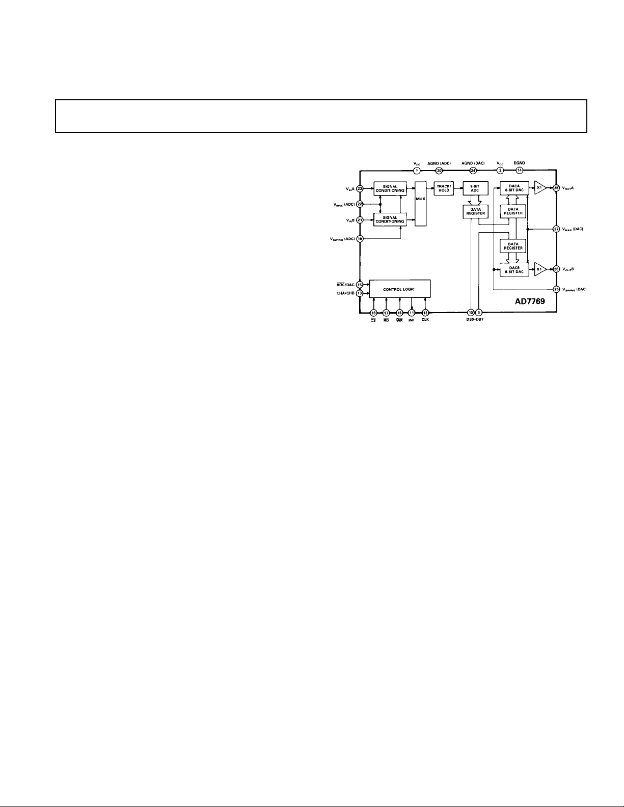
The AD7769 is a complete, two-channel, 8-bit, analog I/O port.
It has versatile input and output signal conditioning features
that make it ideal for use in head-positioning servos in Winchester disk systems. It is equally suitable for floppy disk microstepping head positioning, other closed loop digital servo systems
and general purpose 8-bit data acquisition.
The AD7769 contains a high speed successive approximation
ADC, preceded by a two-channel multiplexer and signal conditioning circuits. The input span of the ADC and the offset of
the zero point from ground can be independently set by applying ground referenced voltages. The AD7769 also contains two
independent, fast settling, 8-bit DACs with output amplifiers.
The output span and offset voltage of the DACs can be set independently of those of the ADC. This makes the AD7769 especially useful in disk drives, where only a positive supply rail is
available and the ranges of the ADC and DACs must be referenced to some positive voltage less than the supply.
The AD7769 is easily interfaced to a standard 8-bit mpu bus via
an 8-bit data port and standard microprocessor control lines.
The AD7769 is fabricated in Linear Compatible CMOS
2
(LC
MOS), an advanced, mixed technology process that combines precision bipolar circuits with low power CMOS logic.
The part is available in a 28-lead plastic DIP and 28-terminal
PLCC package.
Analog I/O Port
AD7769
FUNCTIONAL BLOCK DIAGRAM
PRODUCT HIGHLIGHTS
1. Two-Channel, 8-Bit Analog I/O port on a Single Chip.
The AD7769 contains a two-channel, high speed ADC with
input signal conditioning and two, fast settling 8-bit DACs
with output amplifiers, on a single chip.
2. Independent Control of Span and Offset.
The input voltage span of the ADC and the midpoint of the
transfer function, the output voltage swing of the two DACs
and the half-scale output voltage, can be set independently
by applying ground referenced control voltages.
3. Dynamic Specifications for DSP Users.
In addition to the traditional ADC and DAC specifications,
the AD7769 is specified with ac parameters including signalto-noise ratio, distortion and signal bandwidth.
4. Fast Microprocessor Interface.
The AD7769 has bus interface timing compatible with all
modern microprocessors, with bus access and relinquish
times less than 65 ns and a Write pulse width less than 90 ns.
REV. A
Information furnished by Analog Devices is believed to be accurate and
reliable. However, no responsibility is assumed by Analog Devices for its
use, nor for any infringements of patents or other rights of third parties
which may result from its use. No license is granted by implication or
otherwise under any patent or patent rights of Analog Devices.
One Technology Way, P.O. Box 9106, Norwood, MA 02062-9106,U.S.A.
Tel: 617/329-4700 World Wide Web Site: http://www.analog.comFax:
617/326-8703 © Analog Devices, Inc., 1997
Page 2

AD7769–SPECIFICA TIONS
(VDD = +12 V 6 10%; VCC = +5 V 6 5%; AGND [ADC] = AGND [DAC] = DGND = 0 V; V
ADC SPECIFICATIONS
V
[ADC] = +2.5 V; f
SWING
= 5 MHz external. All specifications T
CLK
MIN
Parameter J Version A Version Units Conditions/Comments
DC ACCURACY
Resolution 8 * Bits
Relative Accuracy ±1 * LSB max See Terminology
Differential Nonlinearity ±1 * LSB max No Missing Codes. See Terminology.
Bias Offset Error See Terminology
+25°C ±2.5 * LSB max
T
MIN
to T
MAX
±3.0 * LSB max
Bias Offset Match Channel A to Channel B
+25°C ±2.5 * LSB max
T
MIN
to T
MAX
±3.5 * LSB max
Plus or Minus Full-Scale Error See Terminology
+25°C ±2.0 * LSB max
T
MIN
to T
MAX
±2.5 * LSB max
Plus or Minus Full-Scale Match Channel A to Channel B
+25°C ±3.5 * LSB max
T
to T
MIN
MAX
ADC TO DAC MATCHING Channel A/B to V
Bias Offset Match V
±4 * LSB max
(DAC) = +5 V, V
BIAS
OUT
A/B
SWING
+25°C ±2.5 * LSB max
T
MIN
to T
MAX
±3.5 * LSB max
Plus or Minus Full-Scale Match
+25°C ±3.5 * LSB max
T
to T
MIN
MAX
DYNAMIC PERFORMANCE
±4.0 * LSB max
2
Signal-to-Noise Ratio (SNR) 44 * dB min VIN = 100 kHz Full-Scale Sine Wave with f
Total Harmonic Distortion (THD) 48 * dB max VIN = 100 kHz Full-Scale Sine Wave with f
Intermodulation Distortion (IMD) 60 * dB typ f
= 99 kHz, fb = 96.7 kHz with f
a
Frequency Response 0.1 * dB typ VIN = Full-Scale, dc to 200 kHz Sine Wave
ANALOG INPUTS
Input Voltage Ranges, V
A, VINBV
IN
V
BIAS
BIAS
– V
+ V
or 0 V min Whichever Is the Higher
SWING
or 9.8 V max Whichever Is the Lower
SWING
Input Currents, IINA, IINB ±0.4 * mA max
ADC REFERENCE INPUTS
Input Voltage Levels
V
(ADC) 2/6.8 * V min/max With Respect to AGND (ADC). For Specified Performance.
BIAS
V
(ADC) 2.0/3.0 * V min/max With Respect to AGND (ADC). For Specified Performance.
SWING
Input Currents
V
(ADC) Input ±800 * µA max
BIAS
V
(ADC) Input ±1* µA max
SWING
LOGIC OUTPUTS
DB0–DB7,
VOL, Output Low Voltage 0.4 * V max I
V
INT
, Output High Voltage 4.0 * V min I
OH
= 1.6 mA
SINK
SOURCE
= 200 µA
DB0–DB7
Floating State Leakage Current ±10 * µA max
Floating State Capacitance
2
10 * pF max
Output Coding Offset Binary
POWER REQUIREMENTS
V
Range 4.75/5.25 * V min/V max For Specified Performance. The Part Will Function with
CC
VCC =5 V ±10% with Degraded Performance.
V
Range 10.8/13.2 * V min/V max For Specified Performance
DD
I
@ +25°C 20 * mA max For ADC and DAC: V
DD
V
Am VINB = T
UB
MIN
to T
22 * mA max V
MAX
; DAC Code = FF (Hex); DACA and DACB Load = 5 kΩ
BIAS
BIAS
to AGND (DAC). Typically I
I
@ +25°C 5 * mA max Logic Inputs = 2.4 V, CLK Input = 0.8 V. Typically I
CC
T
to T
MIN
MAX
NOTES
1
Temperature range as follows: J Version: 0°C to +70°C; A Version: –40°C to +85°C.
2
Sample tested at +25°C to ensure compliance.
*Specification same as J Version.
Specifications subject to change without notice.
6 * mA max
1
to T
unless otherwise noted.)
MAX
(DAC) = +2.5 V.
SAMPLING
= 5.0 V; V
= 14 mA.
DD
BIAS
SAMPLING
SAMPLlNG
= 400 kHz
= 3.0 V; VINA,
SWING
[ADC] = +5 V;
= 400 kHz
= 400 kHz
= 1.5 mA.
CC
–2–
REV. A
Page 3

AD7769
(VDD = +12 V 6 10%; VCC = +5 V 6 5%; AGND [DAC] = AGND [ADC] = DGND = 0 V;
V
[DAC] = +5 V; V
BIAS
DACA, DACB SPECIFICATIONS
CL = 100 pF. All specifications T
Parameter J Version A Version Units Conditions/Comments
STATIC PERFORMANCE
Resolution 8 * Bits
Relative Accuracy ±1 * LSB max See Terminology
Differential Nonlinearity ±1 * LSB max Guaranteed Monotonic. See Terminology.
Bias Offset Error See Terminology
+25°C ±2.0 * LSB max
to T
T
MIN
MAX
±2.5 * LSB max
Bias Offset Match V
+25°C ±2.5 * LSB max
to T
T
MIN
MAX
±3.5 * LSB max
Plus or Minus Full-Scale Error See Terminology
+25°C ±1.5 * LSB max
to T
T
MIN
MAX
±2.0 * LSB max
Plus or Minus Full-Scale Match V
+25°C ±3.5 * LSB max
T
MIN
to T
MAX
±4.0 * LSB max
ADC to DAC MATCHING As Per ADC Specifications
DYNAMIC PERFORMANCE
2
Signal-to-Noise Ratio (SNR) 44 * dB min V
Total Harmonic Distortion (THD) 48 * dB max V
Intermodulation Distortion (IMD) 55 * dB typ fa = 18.4 kHz, fb = 14.5 kHz with f
ANALOG OUTPUTS
Output Voltage Ranges
A, V
V
OUT
BV
OUT
DC Output Impedance 0.5 *
– V
BIAS
+ V
V
BIAS
–2.0 V max Whichever Is the Lower
V
DD
or 0.5 V min Whichever Is the Higher
SWING
or
SWING
Ω
typ
Short-Circuit Current 20 * mA typ
DAC REFERENCE INPUTS
Input Voltage Levels
(DAC) 3/6.8 * V min/max With Respect to AGND (DAC). For Specified Performance.
V
BIAS
(DAC) 2.0/3.0 * V min/max With Respect to AGND (DAC). For Specified Performance.
V
SWING
Input Currents
(DAC) Input ±2* µA max
V
BIAS
V
(DAC) Input ±1* µA max
SWING
AC CHARACTERISTICS
2
Voltage Output Settling Time 4 * µs max Settling Time to Within ±1/2 LSB of Final Value. Typically 2.5 µs.
Digital-to-Analog Glitch Impulse 30 * nV sec typ See Terminology
Digital Feedthrough 1 * nV sec typ See Terminology
LOGIC INPUTS
CS, RD, WR, ADC/DAC,
CHA/CHB, DB0–DB7
Input Low Voltage, V
Input High Voltage, V
INL
INH
0.8 * V max
2.4 * V min
Input Leakage Current ±10 * µA max
Input Capacitance 10 * pF max
CLK
Input Low Voltage 0.8 * V max External Clock. For Internal Clock Operation Connect
Input High Voltage 2.4 * V min the CLK Pin to V
Input Leakage Current ±10 * µA max
DB0–DB7
Input Coding Offset Binary
POWER REQUIREMENTS As per ADC Specifications
NOTES
1
Temperature range as follows: J Version: 0°C to +70°C; A Version: –40 °C to +85 °C.
2
Sample tested at +25°C to ensure compliance.
*Specifications same as J Version.
Specifications subject to change without notice.
[DAC] = +2.5 V; V
SWING
MIN
A to V
OUT
A to V
OUT
= 20 kHz Full-Scale Sine Wave With f
OUT
= 20 kHz Full-Scale Sine Wave With f
OUT
A, V
OUT
OUT
1
to T
unless otherwise noted.)
MAX
B
OUT
B
OUT
.
DD
B load to AGND [DAC], RL = 5 kV,
= 400 kHz
= 400 kHz
SAMPLING
SAMPLING
SAMPLING
= 400 kHz
REV. A
–3–
Page 4
AD7769
(VCC = +5 V 6 5%; VDD = +12 V 6 10%; AGND [ADC] = AGND [DAC] = DGND = 0 V.
TIMING CHARACTERISTICS
Parameter Label +258CT
ADC /DAC CONTROL TIMING
CS to WR Setup Time t
CS to WR Hold Time t
ADC/DAC to WR Setup Time t
ADC/DAC to WR Hold Time t
CHA/CHB to WR Setup Time t
CHA/CHB to WR Hold Time t
WR Pulse Width t
ADC CONVERSION TIMING
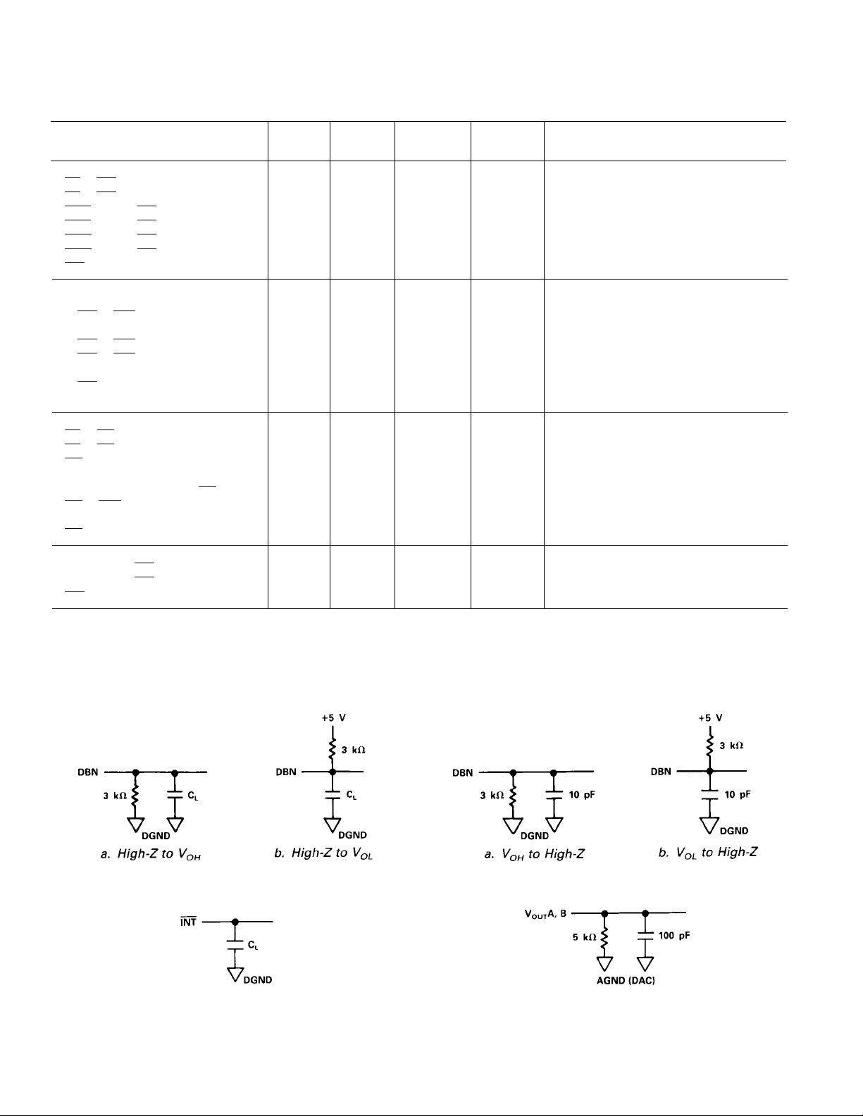
Using External Clock Load Circuit of Figure 3, CL = 20 pF
WR to INT Low Delay t
Using Internal Clock Load Circuit of Figure 3, C
WR to INT Low Delay t
WR to INT High Delay t
WR to Data Valid Delay
ADC READ TIMING
CS to RD Setup Time t
CS to RD Hold Mode t
RD to Data Valid Delay
Bus Relinquish Time after
RD to INT High Delay t
RD Pulse Width t
DAC WRITE TIMING
Data Valid to
Data Valid to
WR Setup Time t
WR Hold Time t
WR to DAC Output Settling Time t
NOTES
1
See Figures 11, 12 and 13.
2
Sample tested at +25°C to ensure compliance. All input signals are specified with tr = tf = 5 ns (10% to 90% of 5 V) and timed from a voltage level of 1.6 V.
3
t10 and t13 are measured with the load circuits of Figure 1 and defined as the time required for an output to cross 0.8 V or 2.4 V.
4
t14 is defined as the time required for the data lines to change 0.5 V when loaded with the circuits of Figure 2.
Specifications subject to change without notice.
3
3
RD High
1, 2
For ADC and DAC, V
Limit at Limit at
1
2
3
4
5
6
7
8
8
9
t
9
t
10
t
10
11
12
t
13
t
4
13
t
14
15
t
15
16
17
18
19
0 0 ns min
0 0 ns min
00 ns
0 0 ns min
0 0 ns min
0 0 ns min
80 80 ns min
2.6 2.6 µs max
1.9/3.0 1.9/3.0 µs min/max Typically 2.5 µs
85 85 ns max Load Circuit of Figure 3, CL = 20 pF
120 120 ns max Load Circuit of Figure 3, CL = 100 pF
t8+70 t8+70 ns max Load Circuit of Figure 1, CL = 20 pF
t8+110 t8+110 ns max Load Circuit of Figure 1, CL = 100 pF
0 0 ns min
0 0 ns min
15/65 15/65 ns min/max Load Circuit of Figure 1, CL = 20 pF
30/100 30/100 ns min/max Load Circuit of Figure 1, CL = 100 pF
15/65 15/65 ns min/max Load Circuit of Figure 2
80 80 ns max Load Circuit of Figure 3, CL = 20 pF
110 110 ns max Load Circuit of Figure 3, CL = 100 pF
t
13
65 65 ns nıin
15 20 ns min
44 µs max Load Circuit of Figure 4
= +5 V, V
BIAS
MIN
t
13
, T
= +2.5 V.)
SWING
Units Test Conditions/Comments
MAX
ns min Determined by t
13
= 20 pF
L
Figure 1. Load Circuits for Data Access Time Test
Figure 3. Load Circuit for
RD
and WR to
INT
Delay Test
–4–
Figure 2. Load Circuits for Bus Relinquish Time Test
Figure 4. Load Circuit for DAC Settling Time Test
REV. A
Page 5

AD7769
WARNING!
ESD SENSITIVE DEVICE
ABSOLUTE MAXIMUM RATINGS*
VDD to AGND or DGND . . . . . . . . . . . . . . . . .–0.3 V, +15 V
V
to DGND . . . . . . . . . . . . . . . . –0.3 V, VDD +0.3 V or 7 V
CC
(Whichever is Lower)
AGND to DGND . . . . . . . . . . . . . . . . . . –0.3 V, V
+0.3 V
DD
Power Dissipation (Any Package)
to +75°C . . . . . . . . . . . . . . . . . . . . . . . . . . . . . . . . 500 mW
Derates Above +75°C by . . . . . . . . . . . . . . . . . . . 6 mW/°C
Storage Temperature Range . . . . . . . . . . . . –65°C to +150°C
Lead Temperature (Soldering 10 secs) . . . . . . . . . . . .+300°C
Digital Inputs to DGND
(Pins 12, 13, 15–18) . . . . . . . . . . . . . . –0.3 V, V
Digital Outputs to DGND
(Pins 3–10, 11) . . . . . . . . . . . . . . . . . . .–0.3 V, V
Analog Inputs to AGND . . . . . . . . . . . . . –0.3 V, V
Analog Outputs to AGND . . . . . . . . . . . . –0.3 V, V
+0.3 V
DD
+0.3 V
CC
+0.3 V
DD
+0.3 V
DD
*Stresses above those listed under Absolute Maximum Ratings may cause perma-
nent damage to the device. This is a stress rating only; functional operation of the
device at these or any other conditions above those listed in the operational
sections of this specification is not implied. Exposure to absolute maximum rating
conditions for extended periods may affect device reliability. Only one Absolute
Maximum Rating may be applied at any one time.
Operating Temperature Range
Commercial (J Version) . . . . . . . . . . . . . . . . . 0°C to +70°C
Industrial (A Version) . . . . . . . . . . . . . . . . –40°C to +85°C
CAUTION
ESD (electrostatic discharge) sensitive device. Electrostatic charges as high as 4000 V readily
accumulate on the human body and test equipment and can discharge without detection.
Although the AD7769 features proprietary ESD protection circuitry, permanent damage may
occur on devices subjected to high energy electrostatic discharges. Therefore, proper ESD
precautions are recommended to avoid performance degradation or loss of functionality.
ORDERING GUIDE
Temperature Package
Model Range Option*
NOTE
Do not allow V
to exceed VDD by more than 0.3 V. In cases
CC
where this can happen the diode protection scheme shown
below is recommended.
AD7769JN 0°C to +70°C N-28
AD7769JP 0 °C to +70°C P-28A
AD7769AN –40°C to +85°C N-28
AD7769AP –40°C to +85°C P-28A
*N = Plastic DIP; P = Plastic Leaded Chip Carrier.
PIN CONFIGURATIONS
DIP PLCC
REV. A
–5–
Page 6

AD7769
PIN FUNCTION DESCRIPTION
Pin Mnemonic Description
1V
2V
DD
CC
+12 V Power Supply. This powers the analog circuitry.
+5 V Power Supply. This powers the logic circuitry.
3–10 DB7–DB0 Input/Output Data Bus. A bidirectional data port from which ADC output data may be read
and to which DAC input data may be written. DB7 is the Most Significant Bit.
11
INT Interrupt Output (active low). INT is set high on the falling edge of RD or WR to the ADC
and goes low at the end of a conversion.
12 CLK Clock input. A clock is required for the ADC. An external TTL-compatible clock may be applied to
this input pin. Alternatively, tying this pin to V
enables the internal clock oscillator. With an
DD
external clock, the mark-space ratio can vary from 30/70 to 70/30.
13 CHA/CHB Channel A/Channel B Select Input. Selects Channel A or Channel B of the DAC or ADC.
Used in conjunction with
WR, RD, CS and ADC/DAC for read or write operations.
14 DGND Digital Ground.
15
16
ADC/DAC ADC or DAC Select Input. Selects either the ADC or the DAC for read or write operations in
conjunction with
WR, RD, CS and CHA/CHB.
WR Write Input (edge triggered). This is used in conjunction with the ADC/DAC, CHA/CHB and CS
control inputs to start an ADC conversion or write data to the DAC. An ADC conversion starts on the
17
18
19 V
rising edge of
RD Read Input (active low). This input must be low to access data from the ADC.
CS Chip Select Input (active low). The device is selected when this input is low.
(ADC) ADC Reference Input. The voltage applied to this pin with respect to AGND (ADC) sets the
SWING
in put voltage Full-Scale Range (FSR) of the ADC. V
WR.
(FSR) = 2 V
IN
SWING
(ADC).
20 AGND (ADC) ADC Analog Ground.
21 V
22 V
B Analog Input for Channel B. See VINA description.
IN
(ADC) ADC Reference Input. The voltage applied to this pin with respect to AGND (ADC) sets the
BIAS
midpoint of the ADC transfer function.
23 V
A Analog Input for Channel A. The input voltage range of both ADC channels is given by:
IN
V
A/B = V
IN
(ADC) ±V
BIAS
SWING
(ADC).
24 AGND (DAC) DAC Analog Ground.
25 V
26 V
27 V
(DAC) DAC Reference Input. The voltage applied to this pin with respect to AGND (DAC) sets the
SWING
B Analog Output Voltage from DAC B. See V
OUT
(DAC) DAC Reference Input. The voltage applied to this pin with respect to AGND (DAC) sets the
BIAS
output voltage Full-Scale Range (FSR) of the DACs. V
OUT
OUT
A description.
(FSR) = 2 V
SWING
(DAC).
midpoint output voltage of the DACs.
28 V
A Analog Output Voltage from DAC A. The output voltage range of both DACs is given by:
OUT
V
OUT
A/B = V
(DAC) ± V
BIAS
SWING
(DAC).
TERMINOLOGY
Relative Accuracy
For an ADC, Relative Accuracy or endpoint nonlinearity is the
maximum deviation, in LSBs, of the ADC’s actual code transition points from a straight line drawn between the endpoints of
the ADC transfer function, i.e., the 00 to 01 and FE to FF Hex
(01111111 to 11111111 Binary) code transitions.
For a DAC, Relative Accuracy or endpoint nonlinearity is a
measure of the maximum deviation, in LSBs, from a straight
line passing through the endpoints of the DAC transfer function, i.e., those voltages which correspond to codes 00 and FF
Hex.
For the specified input and output ranges, 1 LSB = 19.5 mV,
but will vary with V
1 LSB = 2 V
SWING
. For both DACs and ADC,
SWING
/256 = FSR/256.
–6–
Differential Nonlinearity
Differential Nonlinearity is the difference between the measured
change and the ideal 1 LSB change between any two adjacent
codes. A specified differential nonlinearity of ± 1 LSB max ensures monotonicity (DAC) or no missed codes (ADC).
Bias Offset Error
For an ideal ADC, the output code for an input voltage equal to
V
(ADC), should be 80 Hex (10000000 binary). The ADC
BIAS
Bias Offset Error is the difference between the actual midpoint
voltage for code 80 Hex and V
(ADC), expressed in LSBs.
BIAS
For an ideal DAC, the output voltage for code 80 Hex should
be equal to V
difference between the actual output voltage and V
(DAC). The DAC Bias Offset Error is the
BIAS
BIAS
(DAC),
expressed in LSBs.
REV. A
Page 7

AD7769
Plus and Minus Full-Scale Error
The ADC and DACs in the AD7769 can be considered as devices with bipolar (plus and minus) input ranges, but referred to
V
instead of AGND. Plus Full-Scale Error for the ADC is the
BIAS
difference between the actual input voltage at the FE to FF code
transition and the ideal input voltage (V
BIAS
+ V
SWING
–1.5 LSB),
expressed in LSBs. Minus Full-Scale Error is similarly specified
for the 01 to 00 code transition, relative to the ideal input voltage
for this transition (V
BIAS
– V
+0.5 LSB). Plus Full-Scale
SWING
Error for the DACs is the difference, expressed in LSBs, between
the actual output voltage for input code FF and the ideal voltage
(V
+ V
BIAS
specified for code 00, relative to the ideal output voltage (V
V
). Note that Plus and Minus Full-Scale errors for the
SWING
– 1 LSB). Minus Full-Scale Error is similarly
SWING
BIAS
–
ADC and the DAC outputs are measured after their respective
Bias Offset errors have been adjusted out.
Digital-to-Analog Glitch Impulse
Digital-to-Analog Glitch Impulse is the impulse injected into the
analog outputs when the digital inputs change state with either
DAC selected. It is normally specified as the area of the glitch in
nV secs and is measured when the digital input code is changed
by 1 LSB at the major carry transition.
Digital Feedthrough
Digital Feedthrough is also a measure of the impulse injected
into the analog outputs from the digital inputs but is measured
when the DACs are not selected. This is essentially feedthrough
across the die and package. It is important in the AD7769 since
it is a measure of the glitch impulse transferred to the analog
outputs when data is read from the ADC register. It is specified
in nV secs and measured with
WR high and a digital code
change from all 0s to all 1s.
Signal-to-Noise Ratio (SNR)
SNR is the measured Signal-to-Noise Ratio at the output of the
converter. The signal is the rms magnitude of the fundamental.
Noise is the rms sum of all the nonfundamental signals up to
half the sampling frequency. SNR is dependent on the number
of quantization levels used in the digitization process; the more
levels, the smaller the quantization noise. The theoretical SNR
for a sine wave is given by
SNR = (6.02N + 1.76) dB
where N is the number of bits. Thus for an ideal 8-bit converter,
SNR = 49.92 dB.
Total Harmonic Distortion (THD)
THD is the ratio of the rms sum of harmonics to the fundamental. For the AD7769, Total Harmonic Distortion is defined as
1/2
2
2
+V
)
6
20 log
(V
2
+V
2
2
2
+V
3
+V
4
5
V
1
where V1 is the rms amplitude of the fundamental and V2,
V
, V4, V5 and V6 are the rms amplitudes of the individual
3
harmonics.
Intermodulation Distortion (IMD)
With inputs consisting of sine waves at two frequencies, fa and
f
, any active device with nonlinearities will create distortion
b
products, of order (m+n), at sum and difference frequencies of
mf
+nfb, where m, n = 0, 1, 2, 3 . . . Intermodulation terms are
a
those for which neither m nor n is equal to zero. For example,
the second order terms include (f
order terms include (2f
), (2fa–fb), (fa+2fb) and (fa–2fb).
a+fb
) and (fa–fb) and the third
a+fb
LOGIC TRUTH TABLE
ADC CHANNEL SELECT AND START CONVERSION
CS ADC/DAC CHA/CHB WR RD DB0–DB7 INT Comments
0 0 X Note 1 Note 1 1
0 0 0 Note 1 Note 1 1 Select ADC Channel A and Start Conversion.
0 0 1 Note 1 Note 1 1 Select ADC Channel B and Start Conversion.
READ ADC DATA
CS ADC/DAC CHA/CHB WR RD DB0–DB7 INT Comments
0 X X X ADC Data 1
0 X X X 0 ADC Data 1 ADC Data on Data Bus.
0 X X X High-Z 1 Data Outputs Impedance.
WRITE TO DACA OR DACB
CS ADC/DAC CHA/CHB WR RD DB0–DB7 INT Comments
01 0 1 µP Data N/C µP Writing Data to DACA.
01 1 1 µP Data N/C µP Writing Data to DACB.
0 1 0 0 ADC Data N/C Data from Last ADC Conversion Will Be Written to DACA.
0 1 1 0 ADC Data N/C Data from Last ADC Conversion Will Be Written to DACB.
1 X X X X High-Z N/C No Operation.
NOTES
1
If RD = 1, DB0–DB7 will remain high impedance. If RD = 0, DB0–DB7 will output previous ADC data. The RD input should not change during a conversion.
2
X = Don’t Care.
3
N/C = No Change.
0 INT Goes Low at End of Conversion.
INT Is Set on Falling Edge of WR.
INT Is Set High on Falling Edge of RD.
REV. A
–7–
Page 8

AD7769
CIRCUIT DESCRIPTION
Analog Inputs and Outputs
The AD7769 provides the analog-to-digital and digital-to-analog
conversion functions required between the microcontroller and
the servo power amplifier in digital servo systems. It is intended
primarily for closed loop head positioning in Winchester disk
drives, but may also be used for microstepping in drives with
stepper motor head positioning or other servo applications. The
AD7769 contains a high speed, 8-bit, sampling ADC with two
input channels and two 8-bit DACs with output buffer amplifiers. A unique feature of the AD7769 is the input and output signal conditioning circuitry that allows the analog input and
output voltages to be referred to a point other than analog
ground. The input range and offset of the ADC, the output
swing and offset of the DACs may be adjusted independently by
the application of ground-referenced, positive control voltages,
V
(ADC), V
BIAS
SWING
(ADC), V
(DAC) and V
BIAS
SWING
(DAC).
Thus, for example, the peak-to-peak output swing of the DACs
could be set to 3 V above and 3 V below a bias voltage of 5 V.
Figures 5 and 6 show the transfer functions of the ADC
and DACs and their relationship to V
BIAS
and V
SWING.
The
midpoint code of the ADC, 80 Hex (10000000 Binary), occurs
at an input voltage equal to V
equal to 2 V
, so that the Plus Full-Scale code transition
SWING
(FE to FF Hex) occurs at a voltage equal to V
. The input FSR of the ADC is
BIAS
+ V
BIAS
SWING
–1.5 LSBs and the Minus Full-Scale code transition (01 to 00
Hex) occurs at a voltage V
BIAS
– V
+0.5 LSBs. The
SWING
transfer function of the DACs bears a similar relationship to
V
and V
BIAS
(10000000 binary) is equal to V
binary) gives an output voltage of V
(Plus Full-Scale) and 00 Hex gives an output voltage of V
V
(Minus Full-Scale).
SWING
. The DAC output voltage for code 80 Hex
SWING
, while FF Hex (11111111
BIAS
BIAS
+ V
SWING
–1 LSB
BIAS
–
The ability to refer input and output signals to some voltage
other than ground is of particular importance in disk drive applications. Typically, only +5 V digital and +12 V analog supply
voltages are available, and the analog signals are often referred
to a voltage around half the analog supply.
Driving the Analog Inputs and Reference Inputs
The analog inputs, VINA and VINB, must be driven from low
output impedance sources, such as from op amps. In addition,
V
(ADC) must be driven from a similar type low impedance
BIAS
source (e.g., voltage reference).
Op amps are not required to drive the V
(DAC) and V
(DAC) inputs as these are high impedance
SWING
SWING
(ADC), V
BIAS
inputs (200 nA typical input current) that feed into on-chip
buffer amplifiers. The reference voltages for these inputs can be
derived using suitable resistor divider networks.
The analog reference available in the disk drive system can be
used to set the bias voltage of the AD7769, and could also be attenuated to provide the reference for the input and output swing
as shown in Figure 7. The same bias voltage would generally
(though not necessarily) be used for the ADC and the DACs,
though the input and output ranges might be different.
Figure 5. ADC Transfer Function
Figure 6. DAC Transfer Function
Figure 7. Typical Analog Connections to the AD7769
ADC Conversion Cycle
Figure 8 shows the operating waveforms for a conversion cycle.
On the rising edge of
acquisition and tracking of the selected ADC channel, V
V
B. The analog input voltage is held 50 ns (typically) after the
IN
WR, the conversion cycle starts with the
A or
IN
fourth falling edge of the input CLK following a conversion
start. If t
in Figure 8 is greater than 150 ns, then the falling
D
edge of the input CLK will be seen as the first falling clock edge.
If t
is less than 150 ns, the first falling clock edge to be recog-
D
nized will not occur until one cycle later.
–8–
REV. A
Page 9

Figure 8. Operating Waveforms Using External Clock
Following the “hold” on the analog input, the MSB decision is
made approximately 50 ns after the next falling edge of the input CLK. The succeeding bit decisions are made approximately 50 ns after a CLK edge until conversion is complete. At
the end of conversion, the
after the LSB decision and the SAR contents are transferred to
the output latch. The SAR is then reset in readiness for a new
conversion.
Track-and-Hold
The track-and-hold (T/H) amplifier on the analog input to the
ADC of the AD7769 allows the ADC to accurately convert an
input sine wave of 5 V peak-to-peak amplitude up to a frequency of 200 kHz, the Nyquist frequency of the ADC when
operated at its maximum throughput rate of 400 kHz. This
maximum rate of conversion includes conversion time and time
between conversions. Because the input bandwidth of the trackand-hold is much greater than 200 kHz, the input signal should
be band limited to avoid folding unwanted signals into the band
of interest.
DAC Outputs
The D/A converter outputs are buffered with on-board, high
speed op amps that are capable of driving 5 kΩ and 100 pF
loads to AGND (DAC). Each output amplifier settles to within
1/2 LSB of its final output value in typically less than 2.5 µs.
See Figures 9 and 10 for waveforms of the typical output settling time performance.
The output noise from the amplifiers with full scale on the
DACs is typically 200 µV peak-to-peak.
Figure 9. Positive-Going Settling Time
INT line goes low 100 ns (typically)
AD7769
Figure 10. Negative-Going Settling Time
Internal / External Clock Operation
The AD7769 can be operated on either its own internal clock or
with an externally applied clock signal. For internal clock operation the CLK input must be tied to V
nents are required. The internal clock typically runs at 5 MHz
giving a typical conversion time of 2.5 µs. For external clock op-
eration the CLK input must be driven with a TTL/ HCMOS
compatible input. The mark/space ratio of the clock signal can
vary from 30/70 to 70/30. For an input frequency of 5 MHz, the
conversion time is 2.5 µs.
Digital Inputs and Outputs
The AD7769 communicates over a standard, 8-bit microprocessor data bus and is controlled by standard mpu control lines,
CS, WR, RD, INT, plus two address lines, ADC/DAC and
CHA/CHB, which select the DAC or ADC function and Chan-
nel A or Channel B input/output channel. The Chip Select (
line selects the device, Write (
versions or to write data to the DAC, depending on the state of
ADC/DAC. INT is a status flag that indicates completion of a
conversion, while
8-bit data port (DB0–DB7) is a bidirectional port into which
data can be written to the two DAC registers, and from which
data can be read from the ADC register. ADC output data may
also be written directly into either of the DAC registers.
These logical operations are detailed in Table I and in the time
ing diagrams, Figures 11 to 13. Figures 12 and 13 show the
fairly straightforward operations of reading ADC data and writing data to the DACs, and need little explanation. Figure 11
shows the timing for ADC channel selection and conversion
start. This is more complicated as the state of the data outputs
during a conversion depends on
To initiate a conversion (or any other operation) the device
must be selected by taking
taking
WR low, then high again (conversion starts on rising edge
of
WR). There are three possibilities for the state of the data
outputs during the conversion.
1. If
RD is held high, the data outputs will be high impedance
throughout the conversion.
2. If
RD and CS are both held low until after INT goes low,
then DB0–DB7 will initially output data from the last conversion. After
appear on DB0–DB7.
RD is used to read ADC output data. The
INT goes low the new conversion data will
WR) is used to initiate ADC con-
CS low. A conversion is started by
. No external compo-
DD
CS and RD.
CS)
REV. A
–9–
Page 10

AD7769
3. If RD is held low but CS is taken high during the conversion,
the device will be de-selected and DB0–DB7 will revert to
their high impedance state. This will not affect completion of
the conversion, but the data cannot be read, or any other
operation performed, until
4. Note that the state of
CS is taken low again.
RD should not be changed during a
conversion.
Figure 11. Timing for ADC Channel Select and Conversion
Start
DIGITAL SIGNAL PROCESSING APPLICATIONS
In Digital Signal Processing (DSP) application areas like voice
recognition, echo cancellation and adaptive filtering, the dynamic characteristics (SNR, Harmonic Distortion, Intermodulation Distortion) of both the ADC and DACs are critical. The
AD7769 is specified dynamically as well as with standard dc
specifications. Because the track/hold amplifier has a wide bandwidth, an antialiasing filter should be placed on the V
V
B inputs to avoid aliasing of high frequency noise back into
IN
A and
IN
the bands of interest.
The dynamic performance of the ADC is evaluated by applying
a sine wave signal of very low distortion to the V
A or VINB
IN
input which is sampled at a 409.6 kHz sampling rate. A Fast
Fourier Transform (FFT) plot or Histogram plot is then generated from which SNR, harmonic distortion and dynamic differential nonlinearity data can be obtained. For the DACs, the
codes for an ideal sine wave are stored in PROM and loaded
down to the DAC. The output spectrum is analyzed, using a
spectrum analyzer to evaluate SNR and harmonic distortion
performance. Similarly, for intermodulation distortion, an input
(either to VIN or DAC code) consisting of pure sine waves at
two frequencies is applied to the AD7769.
Figure 14 shows a 2048 point FFT plot of the ADC with an input signal of 130 kHz. The SNR is 49.2 dB. It can be seen that
most of the harmonics are buried in the noise floor. It should be
noted that the harmonics are taken into account when calculating the SNR. The relationship between SNR and resolution (N)
is expressed by the following equation:
SNR = (6.02N + 1.76) dB
Figure 12. Timing for ADC Data Read
Figure 13. Timing for DAC Channel Select and Data Write
–10–
Figure 14. ADC FFT Plot
REV. A
Page 11

AD7769
This is for an ideal part with no differential or integral linearity
errors. These errors will cause a degradation in SNR. By working backwards from the above equation, it is possible to get a
measure of ADC performance expressed in effective number of
bits (N). The effective number of bits is plotted versus frequency in Figure 15. The effective number of bits typically falls
between 7.7 and 7.9, corresponding to SNR Figures 48.1 and
49.7 dB.
Figure 15. Effective Number of Bits vs. Frequency
Figure 16 shows a spectrum analyzer plot of the output spectrum from one of the DACs with an ideal sine wave table loaded
to the data inputs of the DAC. In this case, the SNR is 47 dB.
where A is the peak amplitude of the sine wave and p (V) the
probability of occurrence at a voltage V. The histogram plot of
Figure 17 corresponds very well with this shape.
Figure 17. ADC Histogram Plot
In digital signal processing applications, where the AD7769 is
used to sample ac signals, it is essential that the signal sampling
occurs at exactly equal intervals. This minimizes errors due to
sampling uncertainty or jitter. A precise timer or clock source,
to start the conversion process, is the best method of generating
equidistant sampling intervals.
Figure 16. DAC Output Spectrum
Histogram Plot
When a sine wave of specified frequency is applied to the VINA
or V
B input of the AD7769 and several thousand samples are
IN
taken, it is possible to plot a histogram showing the frequency of
occurrence of each of the 256 ADC codes. If a particular step is
wider than the ideal 1 LSB width, then the code associated with
that step will accumulate more counts than for the code for an
ideal step. Likewise, a step narrower than ideal width will have
fewer counts. Missing codes are easily seen because a missing
code means zero counts for a particular code. The absence of
large spikes in the plot indicates small differential nonlinearity.
Figure 17 shows a histogram plot for the ADC indicating very
small differential nonlinearity and no missing codes for an input
frequency of 204 kHz. For a sine wave input, a perfect ADC
would produce a probability density function described by the
equation:
p (V) =
π(A
1
2
–V2)
1/2
MICROPROCESSOR/MICROCOMPUTER INTERFACING
The AD7769 is designed for easy interfacing to microprocessors
and microcomputers as a memory mapped peripheral or an I/O
device. In addition, the AD7769 high speed bus timing allows
direct interfacing to many DSP processors such as the
TMS320C10 and ADSP-2101.
AD7769–TMS320C10 Interface
A typical interface to the TMS320C10 is shown in Figure 18.
The AD7769 is mapped at a port address, and the interface is
designed for the maximum TMS320C10 clock frequency of
20 MHz.
Figure 18. AD7769 to TMS320C10 Interface
REV. A
–11–
Page 12

AD7769
Conversion is initiated on the selected AD7769 ADC channel
using a single I/O instruction, <OUT ADC, A>. The processor
then polls
result using an <IN A, ADC> instruction. Writing data to the relevant AD7769 DAC consists of an <OUT DAC, A> instruction.
AD7769–ADSP-2101 Interface
Figure 19 shows a typical interface to the DSP microcomputer,
the ADSP-2101. The ADSP-2101 is optimized for high speed
numeric processing tasks.
INT until it goes low before reading the conversion
Figure 20. AD7769 to 8051 (Processor Bus) Interface
Figure 19. AD7769 to ADSP-2101 Interface
Because the instruction cycle of the ADSP-2101 is very fast
(80 ns cycle), the
suit the AD7769. This is easily achieved as the ADSP-2101
memory interface supports slower memories and memorymapped peripherals (i.e., AD7769) with a programmable wait
state generation capability. A number of wait states, from 0 to 7,
can be specified for each memory interface. One wait state is
sufficient for the interface to the AD7769.
AD7769–8051 Interface
A choice of two interface modes are available to the 8051
microcomputer.
Figure 20 shows a typical interface to the 8051 processor bus. It
is suitable for the maximum 8051 clock frequency of 12 MHz.
In this interface mode, Port 0 provides the multiplexed low order address and data bus and Port 2 provides the high order address bus (A
Figure 21 shows the AD7769 interfaced to the 8051 parallel I/O
ports. This interface circuit is simpler to implement than the
previous interface to the processor bus, but, in general, the
maximum data throughput rate is much slower (for the same
clock frequencies). In addition to its simplicity, the interface to
the parallel I/O ports versus the processor bus allows independent control of both the
For example, the 8051 can set both
same time. This permits data from the last ADC conversion to
be written directly from the ADC register into the selected DAC
register (see Logic Truth Table). This allows very fast transfer
of data from the ADC to the DAC and is a useful feature for
some applications such as a fast, programmable, infinite sampleand-hold function.
WR and RD pulses must be stretched out to
).
8–A15
WR and RD inputs to the AD7769.
WR and RD low at the
Figure 21. AD7769 to 8051 (Parallel l/O Ports) Interface
AD7769–MC68HC11 Interface
Figure 22 shows a typical interface between the AD7769 and the
MC68HC11 microcomputer. This interface is designed for the
maximum MC68HC11 clock speed of 8.4 MHz. The microcomputer is operated in the expanded multiplexed mode, with the
AD7769 as a memory mapped peripheral. The expansion bus is
made up of Ports B and C, and control signals AS and R/
Figure 22. AD7769 to MC68HC11 Interfaced
W.
–12–
REV. A
Page 13

APPLICATIONS
The AD7769 analog I/O port is used to convert servo related
signals between the analog and digital domains. The input
structure of the two-channel ADC makes it very easy to convert
the typical output signals provided by a servo demodulator.
In a magnetic disk drive employing a dedicated servo surface,
the servo demodulator produces two, positive-only, quadrature
signals, generally sinusoidal or triangular, from the all-bit patterns read from the servo surface. The quadrature signals have
the form of V
BIAS
± V
. The very fast conversion time of the
SWING
AD7769 ADC allows sequential conversion of these quadrature
signals without introducing significant phase delay errors. These
converted signals provide the servo microcontroller with position and track crossing information from which velocity information can be derived. In optical disk drives, analogous servo
signals can be derived from the quad photodiode detector to
provide position and focus information for the microcontroller.
The two DACs in the AD7769 accept servo data from the
microcontroller to position the head assembly. The DACs provide positive-only output signals of the form V
BIAS
± V
SWING
,
which are ideal for driving voice coil motors. In magnetic disk
drives, a single voice coil motor is used to position the head assembly and one DAC is usually sufficient to drive the motor in
both the seek and track modes. In the seek mode, the DAC can
be used to generate directly the desired analog velocity trajectory which the head must travel in order to achieve minimum
access times. Alternatively, the DAC can generate a servo error
value (computed by the microcontroller) between the actual
head velocity and the desired head velocity. In the track mode,
the DAC can be used to provide a position error signal to keep
the head over the track or to detent the head off track, for such
purposes as thermal compensation and soft error retries. The
second DAC in the AD7769 may be employed in this fine positioning loop. Alternatively, the second DAC can be used to control the speed of the spindle motor via a pulse width modulator.
In optical disk drives two voice coil motors are used, requiring
both DACs of the AD7769–one for the focus servo loop and
one for the radial positioning servo loop.
A typical servo control loop using the AD7769 is shown in Figure 23. In this dedicated servo drive, the servo demodulator converts the servo information bit patterns from the disk into the
standard N and Q (normal and quadrature) servo signals. The
voice coil motor current, I
, is bidirectional and is supplied by the
L
power transconductance amplifier. One input to this amplifier is
held at V
output, V
stage are shown in Figure 24. The transconductance, G
(DAC), while the other input is driven from a DAC
BIAS
A/B. Typical input/output waveforms for this power
OUT
, of the
O
power stage is determined by external sense resistors.
AD7769
Figure 23. Typical Dedicated Servo Control Loop Using
the AD7769
Figure 24. Typical Relationship Between Input Voltage and
Output Current for Transconductance Amplifier
REV. A
–13–
Page 14

AD7769
Increased Resolution DAC Output
Since both V
(DAC) and V
BIAS
(DAC) are common to
SWING
both output channels, the full-scale output voltages of both
channels are nominally identical. However, by adding an external op amp and scaling resistors, it is possible to attenuate the
full-scale output voltage of one (or both) of the DAC outputs to
effectively increase the output voltage resolution. Figure 25
shows channel A being attenuated using a resistor scaling of
10:1. The attenuated output voltage, V
V
OUT
A' = V
BIAS
+ (V
SWING
A', is
OUT
/10)(2DA–1).
The output voltage of Channel B remains at
V
OUT
B = V
BIAS
+ V
SWING
(2DB–1).
DA and DB are fractional representations of the DAC input
codes, e.g., D
V
voltage level of 2 V, the Channel B output span is 4 V
SWING
= NA/256 and DB = NB/256. For example, with a
A
with an LSB size of 15.6 mV and (attenuated) Channel A output span is 400 mV with an LSB size of 1.56 mV. Changing the
resistor scaling in Figure 25 obviously changes the attenuated
full-scale output.
DAC A can be programmed to produce an interpolation function between the 8-bit steps of DAC B to allow, for example,
very smooth velocity profile waveforms to be generated.
Servo Offset Facility
Most dedicated servo disk drives offer an offset facility whereby
some small voltage is injected into the track-following loop. The
purpose of the offset is to move the head to the right or left of its
current on-track position to permit reading of off-track data.
The circuit is shown in Figure 27. With the 10:1 resistor scaling
used in the circuit the output voltage, V
V
= VPE + (V
OUT
SWING
, is
OUT
/10) (2DA–1).
Figure 25. Increasing the DAC Output Voltage Resolution
A single change to the circuit Figure 25 allows the two DAC
outputs to be combined to provide a single analog output with
resolution beyond the standard 8-bits. Figure 26 shows the rearranged circuit. The composite output, V
V
OUT
= V
OUT
B + (V
SWING
, is
OUT
/10)(2DA–1)
or
V
OUT
= V
BIAS
+ V
(2DB–1) + (V
SWING
/10) (2DA–1).
SWING
Figure 27. Servo Offset Facility
With no offset added, V
= VPE, where VPE is the position
OUT
error voltage which the servo loop normally drives to its zero
level, V
. When an offset voltage is supplied by DAC A, the
BIAS
action of the servo is to move the head away from its current
on-track position until the position error voltage is equal and
opposite to the offset voltage. The position of the head about
the track centre is thus programmable.
Programmable Full-Scale Range
The output voltage span of both DACs is determined by the
V
(DAC) voltage level. This is normally supplied from
SWING
some fixed voltage source. However, it is possible to use one of
the DAC channels to generate a programmable V
SWING
voltage
level. The remaining channel will thus have a full-scale range
and LSB size which is software programmable. This circuit is
shown in Figure 28 where V
loop to generate a programmable swing voltage, V
B is used in an implicit feedback
OUT
SWING
(DAC),
for the AD7769 from an external fixed input swing voltage,
V
. Using the 5:1 resistor scaling shown in Figure 28, the
SWING
expression for the AD7669 input swing voltage is
V
V
SWING
(DAC) =
SWING
2D
()
1–
.
–1
B
5
Figure 26. Combined V
OUT
A, V
B Circuit
OUT
–14–
REV. A
Page 15

AD7769
Figure 28. Generating a Software Programmable V
SWING
(DAC)
For example, with a fixed input swing voltage of 2.5 V, the programmable span via DAC B is as follows:
D
= 0: V
B
= 1/2: V
D
B
DB ≈ 1: V
The AD7769 is specified for a V
(DAC) = 2.08
SWING
(DAC) = 2.5 V = V
SWING
(DAC) = 3.125 V
SWING
SWING
(DAC) voltage range
SWING
from 2 V to 3 V, although in practice this range can be extended
while still maintaining monotonic operation.
Closed Loop Microstepping
Microstepping is a popular technique in low density disk drives
(both floppy and hard disk) that allows higher positional resolution of the disk drive head over that obtainable from a full-step
driven stepper motor. Typically, a two-phase stepper motor has
its phase currents driven with a sine-cosine relationship. These
cosinusoidal signals are generated by two DACs driven with the
appropriate data. The resolution of the DACs determines the
number of microsteps into which each full step can be divided.
For example, with a 1.8° full-step motor and a 4-bit DAC, a
microstep size of 0.11° (1.8°/2
n
) is obtainable.
The microstepping technique improves the positioning resolution possible in any control application. However, the positional
accuracy can be significantly worse than that offered by the original full-step accuracy specification due to load torque effects.
To ensure that the increased resolution is usable, it is therefore
necessary to use a closed-loop system where the position of the
disk drive head (or motor) is monitored. The closed-loop system
allows an error between the desired position and the actual position to be monitored and corrected. The correction is achieved
by adjusting the ratio of the phase currents in the motor windings until the required head position is reached.
The AD7769 is ideally suited for the closed-loop microstepping
technique with its dual DACs for positioning the disk drive
head and dual channel ADC for monitoring the position of the
head. A typical circuit for a closed-loop microstepping system is
shown in Figure 29. The DAC waveforms are shown in Figure
30 along with the direction information of clockwise rotation
supplied by the controller.
Figure 29. Typical Closed-Loop Microstepping Circuit
with the AD7769
Figure 30. Typical Control Waveforms for the Microstepping Circuit of Figure 29
A typical transducer would be a moire-fringe transducer which
consists of two gratings, one fixed and one moveable. The relative positions of these two gratings will modulate the amount of
light from a LED which can pass through. In order to derive
head direction information the stationary grating has two sets of
bars, with a 90° phase relationship, and two photo-transistors.
The quadrature sinusoidal output waveforms (N & Q) can be
converted directly by the AD7769.
REV. A
–15–
Page 16

AD7769
Multichannel Expansion
In some applications, more than two analog input channels are
required to be converted by the ADC. Figure 31 shows a circuit
configuration for such an application. The ADG528A is a
latched, B-channel analog multiplexer that is ideally suited for
this application since it is specified for single supply operation
(+12 V ±10%).
The
CS, ADC/DAC and WR inputs of the AD7769 are gated to
drive the
signal is selected on the falling edge of the
signal is latched on the rising edge. Also, on the rising edge of
WR, the AD7769 ADC starts conversion. Therefore, the output
signal of the multiplexer must have settled to within 8-bits over
the duration of the
tion for details). The t
ADG528A thus determines the width of the
WR input of the ADG528A. The multiplexer input
WR pulse while the
WR pulse (see ADC Conversion Cycle sec-
(WR) and settling time of the
ON
WR pulse.
OUTLINE DIMENSIONS
Dimensions shown in inches and (mm).
28-Lead Plastic DIP
(N-28)
C1315a–0–6/97
Figure 31. Multichannel Inputs
28-Lead Plastic Leaded Chip Carrier
(P-28A)
–16–
PRINTED IN U.S.A.
REV. A
 Loading...