Analog Devices AD7706EB, AD7705EB, AD7706BRU, AD7706BR, AD7706BN Datasheet
...
3 V/5 V, 1 mW
a
FEATURES
AD7705: Two Fully Differential Input Channel ADCs
AD7706: Three Pseudo Differential Input Channel ADCs
16 Bits No Missing Codes
0.003% Nonlinearity
Programmable Gain Front End
Gains from 1 to 128
Three-Wire Serial Interface
SPI™, QSPI™, MICROWIRE™ and DSP Compatible
Schmitt Trigger Input on SCLK
Ability to Buffer the Analog Input
2.7 V to 3.3 V or 4.75 V to 5.25 V Operation
Power Dissipation 1 mW max @ 3␣ V
Standby Current 8 A max
16-Lead DIP, 16-Lead SOIC and TSSOP Packages
GENERAL DESCRIPTION
2-/3-Channel 16-Bit, Sigma-Delta ADCs
The AD7705/AD7706 are complete analog front ends for low
frequency measurement applications. These two-/three-channel
devices can accept low level input signals directly from a transducer and produce a serial digital output. They employ a sigmadelta conversion technique to realize up to 16 bits of no missing
codes performance. The selected input signal is applied to a
proprietary programmable gain front end based around an analog modulator. The modulator output is processed by an onchip digital filter. The first notch of this digital filter can be
programmed via an on-chip control register allowing adjustment
of the filter cutoff and output update rate.
The AD7705/AD7706 operate from a single 2.7 V to 3.3 V or
4.75 V to 5.25 V supply. The AD7705 features two fully differential analog input channels while the AD7706 features three
pseudo differential input channels. Both devices feature a differential reference input. Input signal ranges of 0 mV to +20␣ mV
through 0 V to +2.5␣ V can be incorporated on both devices when
operating with a V
of 5 V and a reference of 2.5 V. They can
DD
also handle bipolar input signal ranges of ±20␣ mV through ±2.5␣ V,
which are referenced to the AIN(–) inputs on the AD7705 and to
the COMMON input on the AD7706. The AD7705/AD7706,
with 3 V supply and a 1.225 V reference, can handle unipolar
input signal ranges of 0 mV to +10␣ mV through 0 V to +1.225␣ V.
Its bipolar input signal ranges are ±10␣ mV through ±1.225␣ V.
The AD7705/AD7706 thus perform all signal conditioning and
conversion for a two- or three-channel system.
The AD7705/AD7706 are ideal for use in smart, microcontroller
or DSP-based systems. They feature a serial interface that can
be configured for three-wire operation. Gain settings, signal
polarity and update rate selection can be configured in software
*Protected by U.S. Patent Number 5,134,401.
SPI and QSPI are trademarks of Motorola, Inc.
MICROWIRE is a trademark of National Semiconductor.
REV. A
Information furnished by Analog Devices is believed to be accurate and
reliable. However, no responsibility is assumed by Analog Devices for its
use, nor for any infringements of patents or other rights of third parties
which may result from its use. No license is granted by implication or
otherwise under any patent or patent rights of Analog Devices.
*
SCLK
CS
DIN
DOUT
ANALOG
INPUT
CHANNELS
MCLK IN
MCLK OUT
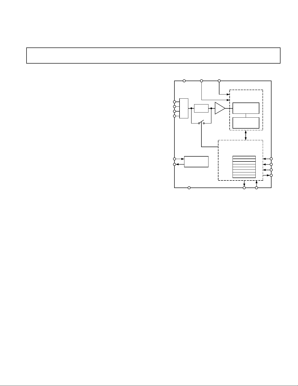
AD7705/AD7706
FUNCTIONAL BLOCK DIAGRAM
V
DD REF IN(–) REF IN(+)
AD7705/AD7706
CHARGE
BALANCING
A/D CONVERTER
MAX
GENERATION
GND
BUFFER
CLOCK
PGA
A = 1<128
SERIAL INTERFACE
S - D
MODULATOR
DIGITAL FILTER
REGISTER BANK
DRDY RESET
using the input serial port. The part contains self-calibration and
system calibration options to eliminate gain and offset errors on
the part itself or in the system.
CMOS construction ensures very low power dissipation, and the
power-down mode reduces the standby power consumption to
20␣ µW typ. These parts are available in a 16-lead, 0.3 inch-wide,
plastic dual-in-line package (DIP), a 16-lead wide body (0.3
inch) small outline (SOIC) package and also a low profile 16lead TSSOP.
PRODUCT HIGHLIGHTS
1. The AD7705/AD7706 consumes less than 1 mW at 3 V
supplies and 1␣ MHz master clock, making it ideal for use in
low power systems. Standby current is less than 8␣ µA.
2. The programmable gain input allows the AD7705/AD7706
to accept input signals directly from a strain gage or transducer, removing a considerable amount of signal conditioning.
3. The AD7705/AD7706 is ideal for microcontroller or DSP
processor applications with a three-wire serial interface reducing the number of interconnect lines and reducing the
number of opto-couplers required in isolated systems.
4. The part features excellent static performance specifications
with 16 bits, no missing codes, ±0.003% accuracy and low
rms noise (<600␣ nV). Endpoint errors and the effects of
temperature drift are eliminated by on-chip calibration options, which remove zero-scale and full-scale errors.
One Technology Way, P.O. Box 9106, Norwood, MA 02062-9106, U.S.A.
Tel: 781/329-4700 World Wide Web Site: http://www.analog.com
Fax: 781/326-8703 © Analog Devices, Inc., 1998

AD7705/AD7706–SPECIFICATIONS
with VDD = 5 V; REF␣ IN(–) = GND; MCLK IN = 2.4576␣ MHz unless otherwise noted. All specifications T
Parameter B Version
1
(VDD = +3 V or 5 V, REF IN(+) = +1.225␣ V with VDD = 3 V and +2.5 V
to T
MIN
Units Conditions/Comments
unless otherwise noted.)
MAX
STATIC PERFORMANCE
No Missing Codes 16 Bits min Guaranteed by Design. Filter Notch < 60␣ Hz
Output Noise See Tables I and III Depends on Filter Cutoffs and Selected Gain
Integral Nonlinearity
Unipolar Offset Error See Note 3
Unipolar Offset Drift
Bipolar Zero Error See Note 3
Bipolar Zero Drift
Positive Full-Scale Error
Full-Scale Drift
Gain Error
Gain Drift
7
4, 8
Bipolar Negative Full-Scale Error
Bipolar Negative Full-Scale Drift
4, 6
2
4
4
5
±0.003 % of FSR max Filter Notch < 60␣ Hz. Typically ±0.0003%
0.5 µV/°C typ
0.5 µV/°C typ For Gains 1, 2 and 4
0.1 µV/°C typ For Gains 8, 16, 32, 64 and 128
See Note 3
0.5 µV/°C typ
See Note 3
2
4
0.5 ppm of FSR/°C typ
±0.003 % of FSR typ Typically ±0.001%
1 µV/°C typ For Gains of 1 to 4
0.6 µV/°C typ For Gains of 8 to 128
ANALOG INPUTS/REFERENCE INPUTS Specifications for AIN and REF IN Unless Noted
Input Common-Mode Rejection (CMR)
V
= 5 V
DD
Gain = 1 96 dB typ
2
Gain = 2 105 dB typ
Gain = 4 110 dB typ
Gain = 8v128 130 dB typ
V
= 3 V
DD
Gain = 1 105 dB typ
Gain = 2 110 dB typ
Gain = 4 120 dB typ
Gain = 8v128 130 dB typ
Normal-Mode 50 Hz Rejection
Normal-Mode 60 Hz Rejection
Common-Mode 50 Hz Rejection
Common-Mode 60 Hz Rejection
Absolute/Common-Mode REF IN Voltage2GND to V
Absolute/Common-Mode AIN Voltage
Absolute/Common-Mode AIN Voltage
AIN DC Input Current
AIN Sampling Capacitance
AIN Differential Voltage Range
AIN Input Sampling Rate, f
Reference Input Range
REF IN(+) – REF IN(–) Voltage 1/1.75 V min/max VDD = 2.7 V to 3.3 V. V
REF IN(+) – REF IN(–) Voltage 1/3.5 V min/max VDD = 4.75 V to 5.25 V. V
REF IN Input Sampling Rate, f
2
2
2
2
2
2
10
S
S
98 dB typ For Filter Notches of 25 Hz, 50 Hz, ±0.02 × f
98 dB typ For Filter Notches of 20 Hz, 60 Hz, ±0.02 × f
150 dB typ For Filter Notches of 25 Hz, 50 Hz, ±0.02 × f
150 dB typ For Filter Notches of 20 Hz, 60 Hz, ±0.02 × f
2, 9
GND – 30 mV V min BUF Bit of Setup Register = 0
VDD + 30␣ mV V max
2, 9
GND + 50␣ mV V min BUF Bit of Setup Register = 1
DD
V min to V max
VDD – 1.5␣ V V max
1 nA max
10 pF max
0 to +V
REF
±V
/GAIN nom Bipolar Input Range (B/U Bit of Setup Register = 0)
REF
GAIN × f
f
/8 For Gains of 8 to 128
CLKIN
11
/GAIN
/64 For Gains of 1 to 4
CLKIN
nom Unipolar Input Range (B/U Bit of Setup Register = 1)
Performance
REF
Performance
f
/64
CLKIN
NOTCH
NOTCH
NOTCH
NOTCH
= 1.225 ± 1% for Specified
= 2.5 ± 1% for Specified
REF
LOGIC INPUTS
Input Current
All Inputs Except MCLK IN ±1 µA max Typically ±20 nA
MCLK ±10 µA max Typically ±2 µA
All Inputs Except SCLK and MCLK IN
V
, Input Low Voltage 0.8 V max VDD = 5 V
INL
V
, Input High Voltage 2.0 V min VDD = 3 V and 5 V
INH
SCLK Only (Schmitt Triggered Input) VDD = 5 V NOMINAL
V
T+
V
T–
VT+ – V
SCLK Only (Schmitt Triggered Input) VDD = 3 V NOMINAL
MCLK IN Only VDD = 5 V NOMINAL
MCLK IN Only VDD = 3 V NOMINAL
T–
V
T+
V
T–
VT+ – V
T–
V
, Input Low Voltage 0.8 V max
INL
V
, Input High Voltage 3.5 V min
INH
V
, Input Low Voltage 0.4 V max
INL
V
, Input High Voltage 2.5 V min
INH
0.4 V max VDD = 3 V
1.4/3 V min/V max
0.8/1.4 V min/V max
0.4/0.8 V min/V max
1/2.5 V min/V max
0.4/1.1 V min/V max
0.375/0.8 V min/V max
–2–
REV. A

AD7705/AD7706
Parameter B Version
LOGIC OUTPUTS (Including MCLK OUT)
VOL, Output Low Voltage 0.4 V max I
VOL, Output Low Voltage 0.4 V max I
VOH, Output High Voltage 4 V min I
VOH, Output High Voltage VDD–0.6 V min I
Floating State Leakage Current ±10 µA max
Floating State Output Capacitance
13
9 pF typ
Data Output Coding Binary Unipolar Mode
Offset Binary Bipolar Mode
SYSTEM CALIBRATION
Positive Full-Scale Calibration Limit
Negative Full-Scale Calibration Limit
Offset Calibration Limit
Input Span
15
14
14
14
(1.05 × V
–(1.05 × V
–(1.05 × V
(0.8 × V
(2.1 × V
POWER REQUIREMENTS
VDD Voltage +2.7 to +3.3 V min to V max For Specified Performance
Power Supply Currents
16
0.32 mA max BUF Bit = 0. f
0.6 mA max BUF Bit = 1. f
0.4 mA max BUF Bit = 0. f
0.6 mA max BUF Bit = 0. f
0.7 mA max BUF Bit = 1. f
1.1 mA max BUF Bit = 1. f
VDD Voltage +4.75 to +5.25 V min to V max For Specified Performance
Power Supply Currents
16
0.45 mA max BUF Bit = 0. f
0.7 mA max BUF Bit = 1. f
0.6 mA max BUF Bit = 0. f
0.85 mA max BUF Bit = 0. f
0.9 mA max BUF Bit = 1. f
Standby (Power-Down) Current
Power Supply Rejection
NOTES
1
Temperature range as follows: B Version, –40°C to +85°C.
2
These numbers are established from characterization or design at initial product release.
3
A calibration is effectively a conversion so these errors will be of the order of the conversion noise shown in Tables I and III. This applies after calibration at the
temperature of interest.
4
Recalibration at any temperature will remove these drift errors.
5
Positive Full-Scale Error includes Zero-Scale Errors (Unipolar Offset Error or Bipolar Zero Error) and applies to both unipolar and bipolar input ranges.
6
Full-Scale Drift includes Zero-Scale Drift (Unipolar Offset Drift or Bipolar Zero Drift) and applies to both unipolar and bipolar input ranges.
7
Gain Error does not include Zero-Scale Errors. It is calculated as Full-Scale Error–Unipolar Offset Error for unipolar ranges and Full-Scale Error–Bipolar Zero Error for
bipolar ranges.
8
Gain Error Drift does not include Unipolar Offset Drift/Bipolar Zero Drift. It is effectively the drift of the part if zero scale calibrations only were performed.
9
This common-mode voltage range is allowed provided that the input voltage on analog inputs does not go more positive than V
GND – 30␣ mV. Parts are functional with voltages down to GND – 200 mV, but with increased leakage at high temperature.
10
The analog input voltage range on AIN(+) is given here with respect to the voltage on AIN(–) on the AD7705 and is given with respect to the COMMON input on the
17
18
AD7706. The absolute voltage on the analog inputs should not go more positive than V
voltages of GND – 200 mV can be accommodated, but with increased leakage at high temperature.
11
V
= REF IN(+) – REF IN(–).
REF
12
These logic output levels apply to the MCLK OUT only when it is loaded with one CMOS load.
13
Sample tested at +25°C to ensure compliance.
14
After calibration, if the analog input exceeds positive full scale, the converter will output all 1s. If the analog input is less than negative full scale, the device will output all 0s.
15
These calibration and span limits apply provided the absolute voltage on the analog inputs does not exceed VDD + 30␣ mV or go more negative than GND – 30␣ mV. The offset
calibration limit applies to both the unipolar zero point and the bipolar zero point.
16
When using a crystal or ceramic resonator across the MCLK pins as the clock source for the device, the VDD current and power dissipation will vary depending on the crystal or
resonator type (see Clocking and Oscillator Circuit section).
17
If the external master clock continues to run in standby mode, the standby current increases to 150␣ µA typical at 5 V and 75 µA at 3 V. When using a crystal or ceramic
resonator across the MCLK pins as the clock source for the device, the internal oscillator continues to run in standby mode and the power dissipation depends on the crystal
or resonator type (see Standby Mode section).
18
Measured at dc and applies in the selected passband. PSRR at 50␣ Hz will exceed 120␣ dB with filter notches of 25 Hz or 50␣ Hz. PSRR at 60␣ Hz will exceed 120␣ dB with filter
notches of 20 Hz or 60␣ Hz.
19
PS
RR depends on both gain and VDD.
1.3 mA max BUF Bit = 1. f
16 µA max External MCLK IN = 0 V or V
8 µA max External MCLK IN = 0 V or V
See Note 19 dB typ
Gain 1 2 4 8–128
VDD = 3 V 86 78 85 93
VDD = 5 V 90 78 84 91
Specifications subject to change without notice.
1
)/GAIN V max GAIN Is the Selected PGA Gain (1 to 128)
REF
)/GAIN V max GAIN Is the Selected PGA Gain (1 to 128)
REF
)/GAIN V max GAIN Is the Selected PGA Gain (1 to 128)
REF
)/GAIN V min GAIN Is the Selected PGA Gain (1 to 128)
REF
)/GAIN V max GAIN Is the Selected PGA Gain (1 to 128)
REF
Units Conditions/Comments
= 800␣ µA Except for MCLK OUT.
SINK
= 100␣ µA Except for MCLK OUT.
SINK
= 200 µA Except for MCLK OUT.
SOURCE
= 100␣ µA Except for MCLK OUT.
SOURCE
Digital I/Ps = 0␣ V or VDD. External MCLK IN and
CLK DIS = 1
= 1␣ MHz. Gains of 1 to 128
CLKIN
= 1␣ MHz. Gains of 1 to 128
CLKIN
= 2.4576␣ MHz. Gains of 1 to 4
CLKIN
= 2.4576␣ MHz. Gains of 8 to 128
CLKIN
= 2.4576␣ MHz. Gains of 1 to 4
CLKIN
= 2.4576␣ MHz. Gains of 8 to 128
CLKIN
Digital I/Ps = 0␣ V or VDD. External MCLK IN and
CLK DIS = 1.
= 1␣ MHz. Gains of 1 to 128
CLKIN
= 1␣ MHz. Gains of 1 to 128
CLKIN
= 2.4576␣ MHz. Gains of 1 to 4
CLKIN
= 2.4576␣ MHz. Gains of 8 to 128
CLKIN
= 2.4576␣ MHz. Gains of 1 to 4
CLKIN
= 2.4576␣ MHz. Gains of 8 to 128
CLKIN
+ 30 mV or go more negative than
DD
+ 30␣ mV, or go more negative than GND␣ – 30␣ mV for specified performance, input
DD
. VDD = 5 V. See Figure 9
DD
. VDD = 3 V
DD
12
VDD = 5 V.
12
VDD = 3 V.
12
VDD = 5 V.
12
VDD = 3 V.
–3–REV. A
AD7705/AD7706
TIMING CHARACTERISTICS
(VDD = +2.7␣ V to +5.25␣ V; GND = 0 V; f
1, 2
unless otherwise noted.)
= 2.4576␣ MHz; Input Logic 0 = 0 V, Logic 1 = V
CLKIN
DD
Limit at T
MIN
, T
MAX
Parameter (B Version) Units Conditions/Comments
3, 4
f
CLKIN
400 kHz min Master Clock Frequency: Crystal Oscillator or Externally Supplied
2.5 MHz max for Specified Performance
t
CLKIN LO
t
CLKIN HI
t
1
t
2
0.4 × t
CLKIN
0.4 × t
CLKIN
500 × t
CLKIN
100 ns min RESET Pulsewidth
ns min Master Clock Input Low Time. t
CLKIN
ns min Master Clock Input High Time
ns nom DRDY High Time
= 1/f
CLKIN
Read Operation
t
3
t
4
5
t
5
t
6
t
7
t
8
6
t
9
t
10
0 ns min DRDY to CS Setup Time
120 ns min CS Falling Edge to SCLK Rising Edge Setup Time
0 ns min SCLK Falling Edge to Data Valid Delay
80 ns max V
100 ns max V
= +5␣ V
DD
= +3.0␣ V
DD
100 ns min SCLK High Pulsewidth
100 ns min SCLK Low Pulsewidth
0 ns min CS Rising Edge to SCLK Rising Edge Hold Time
10 ns min Bus Relinquish Time after SCLK Rising Edge
60 ns max V
100 ns max V
100 ns max SCLK Falling Edge to DRDY High
= +5␣ V
DD
= +3.0␣ V
DD
7
Write Operation
t
11
t
12
t
13
t
14
t
15
t
16
NOTES
1
Sample tested at +25°C to ensure compliance. All input signals are specified with tr = tf = 5 ns (10% to 90% of V
2
See Figures 16 and 17.
3
f
Duty Cycle range is 45% to 55%. f
CLKIN
can draw higher current than specified and possibly become uncalibrated.
4
The AD7705/AD7706 is production tested with f
5
These numbers are measured with the load circuit of Figure 1 and defined as the time required for the output to cross the VOL or VOH limits.
6
These numbers are derived from the measured time taken by the data output to change 0.5␣ V when loaded with the circuit of Figure 1. The measured number is
then extrapolated back to remove effects of charging or discharging the 50 pF capacitor. This means that the times quoted in the timing characteristics are the
true bus relinquish times of the part and as such are independent of external bus loading capacitances.
7
DRDY returns high after the first read from the device after an output update. The same data can be read again, if required, while DRDY is high, although care
should be taken that subsequent reads do not occur close to the next output update.
120 ns min CS Falling Edge to SCLK Rising Edge Setup Time
30 ns min Data Valid to SCLK Rising Edge Setup Time
20 ns min Data Valid to SCLK Rising Edge Hold Time
100 ns min SCLK High Pulsewidth
100 ns min SCLK Low Pulsewidth
0 ns min CS Rising Edge to SCLK Rising Edge Hold Time
) and timed from a voltage level of 1.6 V.
DD
must be supplied whenever the AD7705/AD7706 is not in Standby mode. If no clock is present in this case, the device
CLKIN
at 2.4576␣ MHz (1␣ MHz for some IDD tests). It is guaranteed by characterization to operate at 400␣ kHz.
CLKIN
TO OUTPUT
PIN
50pF
(800mA AT V
I
SINK
100mA AT V
I
(200mA AT VDD = +5V
SOURCE
100mA AT V
+1.6V
DD
DD
= +5V
= +3V)
= +3V)
DD
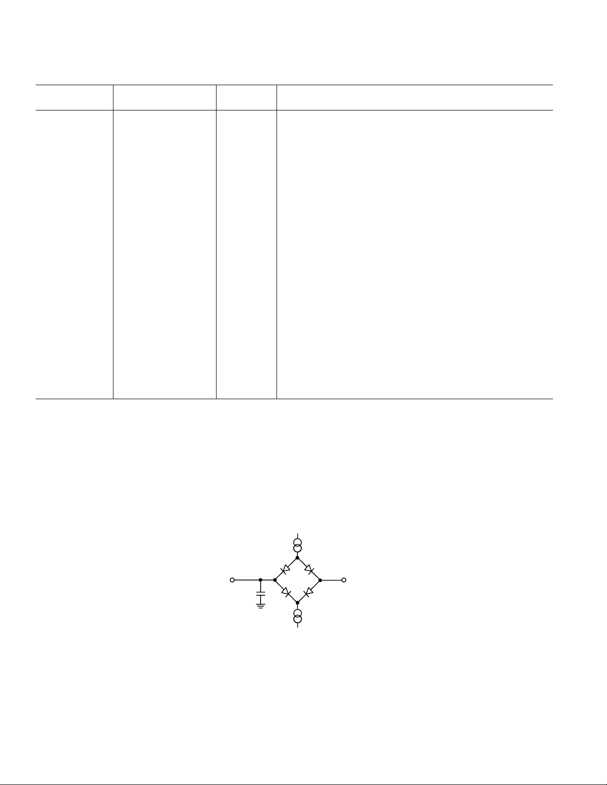
Figure 1. Load Circuit for Access Time and Bus Relinquish Time
–4–
REV. A

AD7705/AD7706
ABSOLUTE MAXIMUM RATINGS*
(T
= +25°C unless otherwise noted)
A
VDD to GND . . . . . . . . . . . . . . . . . . . . . . . . . . –0.3␣ V to +7␣ V
Analog Input Voltage to GND . . . . . . . .–0.3 V to V
Reference Input Voltage to GND . . . . .–0.3 V to V
Digital Input Voltage to GND . . . . . . . .–0.3 V to V
Digital Output Voltage to GND . . . . . .–0.3 V to V
DD
DD
DD
DD
+ 0.3␣ V
+ 0.3␣ V
+ 0.3 V
+ 0.3 V
Operating Temperature Range
Commercial (B Version) . . . . . . . . . . . . . . –40°C to +85°C
Storage Temperature Range . . . . . . . . . . . . –65°C to +150°C
Junction Temperature . . . . . . . . . . . . . . . . . . . . . . . . .+150°C
Plastic DIP Package, Power Dissipation . . . . . . . . . . 450 mW
Thermal Impedance . . . . . . . . . . . . . . . . . . . . 105°C/W
θ
JA
Lead Temperature, (Soldering, 10 sec) . . . . . . . . . .+260°C
SOIC Package, Power Dissipation . . . . . . . . . . . . . . . 450 mW
Thermal Impedance . . . . . . . . . . . . . . . . . . . . . 75°C/W
θ
JA
Lead Temperature, Soldering
Vapor Phase (60 sec) . . . . . . . . . . . . . . . . . . . . . .+215°C
Infrared (15 sec) . . . . . . . . . . . . . . . . . . . . . . . . . .+220°C
SSOP Package, Power Dissipation . . . . . . . . . . . . . . . 450 mW
Thermal Impedance . . . . . . . . . . . . . . . . . . . . 139°C/W
θ
JA
Lead Temperature, Soldering
Vapor Phase (60 sec) . . . . . . . . . . . . . . . . . . . . . .+215°C
␣␣␣␣ Infrared (15 sec) . . . . . . . . . . . . . . . . . . . . . . . . . .+220°C
ESD Rating . . . . . . . . . . . . . . . . . . . . . . . . . . . . . . . . >4000␣ V
*Stresses above those listed under Absolute Maximum Ratings may cause perma-
nent damage to the device. This is a stress rating only; functional operation of the
device at these or any other conditions above those indicated in the operational
section of this specification is not implied. Exposure to absolute maximum rating
conditions for extended periods may affect device reliability.
ORDERING GUIDE
V
DD
Temperature Package Package
Model Supply Range Description Options
AD7705BN 2.7 V to 5.25 V –40°C to +85°C Plastic DIP N-16
AD7705BR 2.7 V to 5.25 V –40°C to +85°C SOIC R-16
AD7705BRU 2.7 V to 5.25 V –40°C to +85°C TSSOP RU-16
EVAL-AD7705EB Evaluation Board
AD7706BN 2.7 V to 5.25 V –40°C to +85°C Plastic DIP N-16
AD7706BR 2.7 V to 5.25 V –40°C to +85°C SOIC R-16
AD7706BRU 2.7 V to 5.25 V –40°C to +85°C TSSOP RU-16
EVAL-AD7706EB Evaluation Board
–5–REV. A
AD7705/AD7706
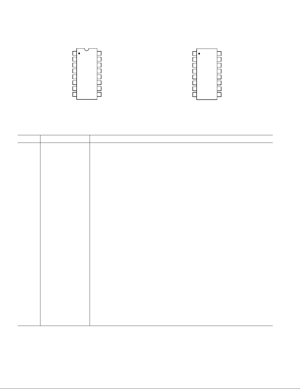
PIN CONFIGURATIONS
SCLK
MCLK IN
MCLK OUT
RESET
AIN2(+)
AIN1(+)
AIN1(–)
CS
1
2
3
AD7705
4
TOP VIEW
5
(Not to Scale)
6
7
8
16
15
14
13
12
11
10
9
GND
V
DD
DIN
DOUT
DRDY
AIN2(–)
REF IN(–)
REF IN(+)
SCLK
MCLK IN
MCLK OUT
CS
RESET
AIN1
AIN2
COMMON
1
2
3
AD7706
4
TOP VIEW
5
(Not to Scale)
6
7
8
16
GND
V
15
DIN
14
13
DOUT
12
DRDY
11
AIN3
10
REF IN(–)
REF IN(+)
9
DD
PIN FUNCTION DESCRIPTIONS
Pin No. Mnemonic Function
1 SCLK Serial Clock. Schmitt-Triggered Logic Input. An external serial clock is applied to this input
to access serial data from the AD7705/AD7706. This serial clock can be a continuous clock
with all data transmitted in a continuous train of pulses. Alternatively, it can be a noncontinuous clock with the information being transmitted to the AD7705/AD7706 in smaller
batches of data.
2 MCLK IN Master Clock signal for the device. This can be provided in the form of a crystal/resonator or
external clock. A crystal/resonator can be tied across the MCLK IN and MCLK OUT pins.
Alternatively, the MCLK IN pin can be driven with a CMOS-compatible clock and MCLK
OUT left unconnected. The part can be operated with clock frequencies in the range
500 kHz to 5 MHz.
3 MCLK OUT When the master clock for the device is a crystal/resonator, the crystal/resonator is connected
between MCLK IN and MCLK␣ OUT. If an external clock is applied to MCLK IN, MCLK
OUT provides an inverted clock signal. This clock can be used to provide a clock source for
external circuitry and is capable of driving one CMOS load. If the user does not require it,
this MCLK OUT can be turned off via the CLK DIS bit of the Clock Register. This ensures
that the part is not burning unnecessary power driving capacitive loads on MCLK OUT.
4 CS Chip Select. Active low Logic Input used to select the AD7705/AD7706. With this input
hard-wired low, the AD7705/AD7706 can operate in its three-wire interface mode with
SCLK, DIN and DOUT used to interface to the device. CS can be used to select the device
in systems with more than one device on the serial bus or as a frame synchronization signal in
communicating with the AD7705/AD7706.
5 RESET Logic Input. Active low input that resets the control logic, interface logic, calibration
coefficients, digital filter and analog modulator of the part to power-on status.
6 AIN2(+)[AIN1] AD7705: Positive input of the differential Analog Input Channel 2. AD7706: Analog Input
Channel 1.
7 AIN1(+)[AIN2] AD7705: Positive input of the differential Analog Input Channel 1. AD7706: Analog Input
Channel 2.
8 AIN1(–)[COMMON] AD7705: Negative input of the differential Analog Input Channel 1. AD7706: COMMON
Input. Analog inputs for Channels 1, 2 and 3 are referenced to this input.
9 REF IN(+) Reference Input. Positive input of the differential Reference Input to the AD7705/AD7706.
The reference input is differential with the provision that REF IN(+) must be greater than
REF IN(–). REF␣ IN(+) can lie anywhere between VDD and GND.
–6–
REV. A
AD7705/AD7706
Pin No. Mnemonic Function
10 REF IN(–) Reference Input. Negative input of the differential reference input to the AD7705/AD7706.
The REF␣ IN(–) can lie anywhere between VDD and GND provided REF␣ IN(+) is greater
than REF␣ IN(–).
11 AIN2(–)[AIN3] AD7705: Negative input of the differential analog Input Channel 2. AD7706: Analog Input
Channel 3.
12 DRDY Logic Output. A logic low on this output indicates that a new output word is available from
the AD7705/AD7706 data register. The DRDY pin will return high upon completion of a
read operation of a full output word. If no data read has taken place between output updates,
the DRDY line will return high for 500 × t
While DRDY is high, a read operation should neither be attempted nor in progress to avoid
reading from the data register as it is being updated. The DRDY line will return low again
when the update has taken place. DRDY is also used to indicate when the AD7705/AD7706
has completed its on-chip calibration sequence.
13 DOUT Serial Data Output with serial data being read from the output shift register on the part. This
output shift register can contain information from the setup register, communications register, clock register or data register, depending on the register selection bits of the Communications Register.
14 DIN Serial Data Input with serial data being written to the input shift register on the part. Data
from this input shift register is transferred to the setup register, clock register or communications register, depending, on the register selection bits of the Communications Register.
15 V
DD
Supply Voltage, +2.7 V to +5.25 V operation.
16 GND Ground reference point for the AD7705/AD7706’s internal circuitry.
cycles prior to the next output update.
CLK␣ IN
OUTPUT NOISE (5 V OPERATION)
Table I shows the AD7705/AD7706 output rms noise for the selectable notch and –3␣ dB frequencies for the part, as selected by FS0
and FS1 of the Clock Register. The numbers given are for the bipolar input ranges with a V
of +2.5␣ V and VDD = 5 V. These
REF
numbers are typical and are generated at an analog input voltage of 0␣ V with the part used in either buffered or unbuffered mode. Table II
meanwhile shows the output peak-to-peak noise for the selectable notch and –3 dB frequencies for the part. It is important to note that
these numbers represent the resolution for which there will be no code flicker. They are not calculated based on rms noise but on peak-to-peak
noise. The numbers given are for bipolar input ranges with a V
of +2.5 V and for either buffered or unbuffered mode. These num-
REF
bers are typical and are rounded to the nearest LSB. The numbers apply for the CLK DIV bit of the Clock Register set to 0.
Table I. Output RMS Noise vs. Gain and Output Update Rate @ 5 V
Filter First Typical Output RMS Noise in V
Notch and O/P –3␣ dB Gain of Gain of Gain of Gain of Gain of Gain of Gain of Gain of
Data Rate Frequency 1248163264128
MCLK IN = 2.4576 MHz
50␣ Hz 13.1␣ Hz 4.1 2.1 1.2 0.75 0.7 0.66 0.63 0.6
60␣ Hz 15.72␣ Hz 5.1 2.5 1.4 0.8 0.75 0.7 0.67 0.62
250␣ Hz 65.5␣ Hz 110 49 31 17 8 3.6 2.3 1.7
500␣ Hz 131␣ Hz 550 285 145 70 41 22 9.1 4.7
MCLK IN = 1 MHz
20␣ Hz 5.24␣ Hz 4.1 2.1 1.2 0.75 0.7 0.66 0.63 0.6
25␣ Hz 6.55␣ Hz 5.1 2.5 1.4 0.8 0.75 0.7 0.67 0.62
100␣ Hz 26.2␣ Hz 110 49 31 17 8 3.6 2.3 1.7
200␣ Hz 52.4␣ Hz 550 285 145 70 41 22 9.1 4.7
–7–REV. A

AD7705/AD7706
Table II. Peak-to-Peak Resolution vs. Gain and Output Update Rate @ 5 V
Filter First Typical Peak-to-Peak Resolution Bits
Notch and O/P –3␣ dB Gain of Gain of Gain of Gain of Gain of Gain of Gain of Gain of
Data Rate Frequency 1248163264128
MCLK IN = 2.4576 MHz
50␣ Hz 13.1␣ Hz 16 16 16 16 16 16 15 14
60␣ Hz 15.72␣ Hz 16 16 16 16 15 14 14 13
250␣ Hz 65.5␣ Hz 13 13 13 13 13 13 12 12
500␣ Hz 131␣ Hz 10 10 10 10 10 10 10 10
MCLK IN = 1 MHz
20␣ Hz 5.24␣ Hz 16 16 16 16 16 16 15 14
25␣ Hz 6.55␣ Hz 16 16 16 16 15 14 14 13
100␣ Hz 26.2␣ Hz 13 13 13 13 13 13 12 12
200␣ Hz 52.4␣ Hz 10 10 10 10 10 10 10 10
OUTPUT NOISE (3 V OPERATION)
Table III shows the AD7705/AD7706 output rms noise for the selectable notch and –3␣ dB frequencies for the part, as selected by
FS0 and FS1 of the Clock Register. The numbers given are for the bipolar input ranges with a V
These numbers are typical and are generated at an analog input voltage of 0␣ V with the part used in either buffered or unbuffered
mode. Table II meanwhile shows the output peak-to-peak noise for the selectable notch and –3 dB frequencies for the part. It is im-
portant to note that these numbers represent the resolution for which there will be no code flicker. They are not calculated based on rms noise but
on peak-to-peak noise. The numbers given are for bipolar input ranges with a V
of +1.225 V and for either buffered or unbuffered
REF
mode. These numbers are typical and are rounded to the nearest LSB. The numbers apply for the CLK DIV bit of the Clock Register set to 0.
of +1.225␣ V and a VDD = 3 V.
REF
Table III. Output RMS Noise vs. Gain and Output Update Rate @ 3 V
Filter First Typical Output RMS Noise in V
Notch and O/P –3␣ dB Gain of Gain of Gain of Gain of Gain of Gain of Gain of Gain of
Data Rate Frequency 1248163264128
MCLK IN = 2.4576 MHz
50␣ Hz 13.1␣ Hz 3.8 2.4 1.5 1.3 1.1 1.0 0.9 0.9
60␣ Hz 15.72␣ Hz 5.1 2.9 1.7 1.5 1.2 1.0 0.9 0.9
250␣ Hz 65.5␣ Hz 50 25 14 9.9 5.1 2.6 2.3 2.0
500␣ Hz 131␣ Hz 270 135 65 41 22 9.7 5.1 3.3
MCLK IN = 1 MHz
20␣ Hz 5.24␣ Hz 3.8 2.4 1.5 1.3 1.1 1.0 0.9 0.9
25␣ Hz 6.55␣ Hz 5.1 2.9 1.7 1.5 1.2 1.0 0.9 0.9
100␣ Hz 26.2␣ Hz 50 25 14 9.9 5.1 2.6 2.3 2.0
200␣ Hz 52.4␣ Hz 270 135 65 41 22 9.7 5.1 3.3
Table IV.␣ Peak-to-Peak Resolution vs. Gain and Output Update Rate @ 3 V
Fi
lter First Typical Peak-to-Peak Resolution in Bits
Notch and O/P –3␣ dB Gain of ␣ Gain of Gain of Gain of Gain of Gain of Gain of Gain of
Data Rate Frequency 1 ␣ ␣ 2 4 8 16 32 64␣␣␣␣ 128
M
CLK IN = 2.4576 MHz
50␣ Hz 13.1␣ Hz 16 16 15 15 14 13 13 12
60␣ Hz 15.72␣ Hz 16 16 15 14 14 13 13 12
250␣ Hz 65.5␣ Hz 13 13 13 13 12 12 11 11
500␣ Hz 131␣ Hz 10 10 10 10 10 10 10 10
MCLK IN = 1 MHz
20␣ Hz 5.24␣ Hz 16 16 15 15 14 13 13 12
25␣ Hz 6.55␣ Hz 16 16 15 14 14 13 13 12
100␣ Hz 26.2␣ Hz 13 13 13 13 12 12 11 11
200␣ Hz 52.4␣ Hz 10 10 10 10 10 10 10 10
–8–
REV. A
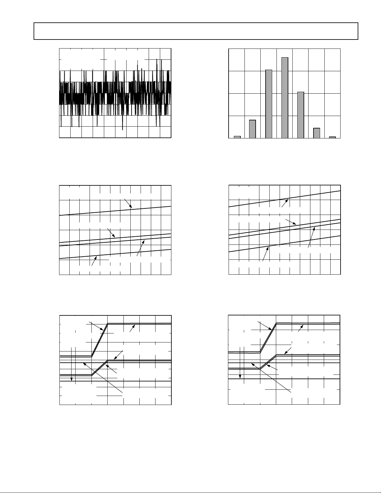
Typical Performance Characteristics–
GAIN
1
I
DD
– mA
VDD = 5V
EXTERNAL MCLK
CLKDIS = 1
TA = +258C
1.2
0.8
0.6
0.4
0.2
0
1.0
248163264128
BUFFERED MODE
f
CLK
= 5MHz,
CLKDIV = 1
BUFFERED MODE
f
CLK
= 1MHz, CLKDIV = 0
BUFFERED MODE
f
CLK
= 2.4576MHz, CLKDIV = 0
UNBUFFERED MODE
f
CLK
= 2.4576MHz, CLKDIV = 0
UNBUFFERED MODE
f
CLK
= 1MHz,
CLKDIV = 0
UNBUFFERED MODE
f
CLK
= 5MHz, CLKDIV = 1
AD7705/AD7706
32771
32770
32769
32768
32767
CODE READ
32766
32765
32764
32763
0 100
VDD = 5V
V
= 2.5V
REF
GAIN = 128
50Hz UPDATE RATE
200 300 400 500 600 700 800 900 1000
TA = +258C
RMS NOISE = 600nV
READING NO.
Figure 2. Typical Noise Plot @ Gain = 128 with 50 Hz
Update Rate
1.2
VDD = 3V
TA = +258C
1.0
0.8
0.6
– mA
DD
I
0.4
0.2
0
0.4
BUFFERED MODE, GAIN = 1
UNBUFFERED MODE, GAIN = 1
0.6 0.8 1.0 1.2 1.4 1.6 1.8 2.0 2.2 2.4 2.6
BUFFERED MODE, GAIN = 128
UNBUFFERED MODE, GAIN = 128
FREQUENCY – MHz
Figure 3. Typical IDD vs. MCLKIN Frequency @ 3 V
400
300
200
OCCURRENCE
100
0
32764
32765 32766 32767 32768 32769 32770
CODE
Figure 5. Histogram of Data in Figure 2
1.2
VDD = 5V
TA = +258C
1.0
0.8
0.6
– mA
DD
I
0.4
0.2
0
0.4
BUFFERED MODE, GAIN = 128
BUFFERED MODE, GAIN = 1
UNBUFFERED MODE, GAIN = 128
UNBUFFERED MODE, GAIN = 1
0.6 0.8 1.0 1.2 1.4 1.6 1.8 2.0 2.2 2.4 2.6
FREQUENCY – MHz
Figure 6. Typical IDD vs. MCLKIN Frequency @ 5 V
1.0
BUFFERED MODE
f
= 5MHz,
CLK
0.9
CLKDIV = 1
0.8
UNBUFFERED MODE
f
= 1MHz,
CLK
0.7
CLKDIV = 0
0.6
0.5
– mA
DD
I
0.4
0.3
VDD = 3V
0.2
EXTERNAL MCLK
CLKDIS = 1
0.1
TA = +258C
0
Figure 4. Typical IDD vs. Gain and Clock Frequency @ 3 V
2 4 8 16 32 64 128
1
BUFFERED MODE
f
= 2.4576MHz, CLKDIV = 0
CLK
UNBUFFERED MODE
f
= 5MHz, CLKDIV = 1
CLK
UNBUFFERED MODE
f
= 2.84MHz, CLKDIV = 0
CLK
BUFFERED MODE
f
= 1MHz, CLKDIV = 0
CLK
GAIN
Figure 7. Typical IDD vs. Gain and Clock Frequency @ 5 V
–9–REV. A
AD7705/AD7706
TEK STOP: SINGLE SEQ 50.0kS/s
V
1
2
2
CH1 5.00V CH2 2.00V
DD
OSCILLATOR = 4.9152 MHz
OSCILLATOR = 2.4576 MHz
5ms/DIV
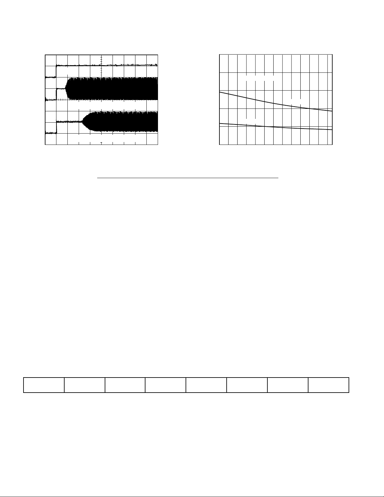
Figure 8. Typical Crystal Oscillator Power-Up Time
20
16
12
8
STANDBY CURRENT – mA
4
0
–40
MCLK IN = 0V OR V
VDD = 3V
–30 –20 –10 0 10 20 30 40 50 60 70 80
DD
VDD = 5V
TEMPERATURE – 8C
Figure 9. Standby Current vs. Temperature
ON-CHIP REGISTERS
The AD7705/AD7706 contains eight on-chip registers which can be accessed via the serial port of the part. The first of these is a
Communications Register that controls the channel selection, decides whether the next operation is a read or write operation and
also decides which register the next read or write operation accesses. All communications to the part must start with a write operation to the Communications Register. After power-on or RESET, the device expects a write to its Communications Register. The
data written to this register determines whether the next operation to the part is a read or a write operation and also determines to
which register this read or write operation occurs. Therefore, write access to any of the other registers on the part starts with a write
operation to the Communications Register followed by a write to the selected register. A read operation from any other register on
the part (including the Communications Register itself and the output data register) starts with a write operation to the Communications Register followed by a read operation from the selected register. The Communications Register also controls the standby mode
and channel selection and the DRDY status is also available by reading from the Communications Register. The second register is a
Setup Register that determines calibration mode, gain setting, bipolar/unipolar operation and buffered mode. The third register is
labelled the Clock Register and contains the filter selection bits and clock control bits. The fourth register is the Data Register from
which the output data from the part is accessed. The final registers are the calibration registers which store channel calibration data.
The registers are discussed in more detail in the following sections.
Communications Register (RS2, RS1, RS0 = 0, 0, 0)
The Communications Register is an 8-bit register from which data can either be read or to which data can be written. All communications to the part must start with a write operation to the Communications Register. The data written to the Communications Register determines whether the next operation is a read or write operation and to which register this operation takes place. Once the
subsequent read or write operation to the selected register is complete, the interface returns to where it expects a write operation to
the Communications Register. This is the default state of the interface, and on power-up or after a RESET, the AD7705/AD7706 is
in this default state waiting for a write operation to the Communications Register. In situations where the interface sequence is lost,
if a write operation of sufficient duration (containing at least 32 serial clock cycles) takes place with DIN high, the AD7705 returns
to this default state. Table V outlines the bit designations for the Communications Register.
Table V.␣ Communications Register
0/DRDY (0) RS2 (0) RS1 (0) RS0 (0) R/W (0) STBY (0) CH1 (0) CH0 (0)
0/DRDY For a write operation, a “0” must be written to this bit so that the write operation to the Communications Register
actually takes place. If a “1” is written to this bit, the part will not clock on to subsequent bits in the register. It
will stay at this bit location until a “0” is written to this bit. Once a “0” is written to this bit, the next seven bits
will be loaded to the Communications Register. For a read operation, this bit provides the status of the DRDY flag
from the part. The status of this bit is the same as the DRDY output pin.
RS2–RS0 Register Selection Bits. These three bits select to which one of eight on-chip registers the next read or write opera-
tion takes place, as shown in Table VI, along with the register size. When the read or write operation to the selected register is complete, the part returns to where it is waiting for a write operation to the Communications
Register. It does not remain in a state where it will continue to access the register.
–10–
REV. A
 Loading...