

2
14 15 7 64 17
AVDDDVDDAVSSDVSSSC1 SC2
13
CALIBRATION
SRAM
16-BIT A/D CONVERTER
ANALOG
MODULATOR
CAL
SLEEP
11
20
19
CLOCK
GENERATOR
SERIAL INTERFACE
LOGIC
SDATA
SCLK
3 2 1 18
CLKIN CLKOUT
MODE
DRDY
6-POLE GAUSSIAN
LOW-PASS
DIGITAL FILTER
AD7701
5DGND
AGND
A
IN
V
REF
8
9
10
BP/UP
12
16
CS
CALIBRATION
MICROCONTROLLER
LC
MOS
16-Bit A/D Converter
AD7701
FEATURES
Monolithic 16-Bit ADC
0.0015% Linearity Error
On-Chip Self-Calibration Circuitry
Programmable Low-Pass Filter
0.1 Hz to 10 Hz Corner Frequency
0 V to +2.5 V or 2.5 V Analog Input Range
4 kSPS Output Data Rate
Flexible Serial Interface
Ultralow Power
APPLICATIONS
Industrial Process Control
Weigh Scales
Portable Instrumentation
Remote Data Acquisition
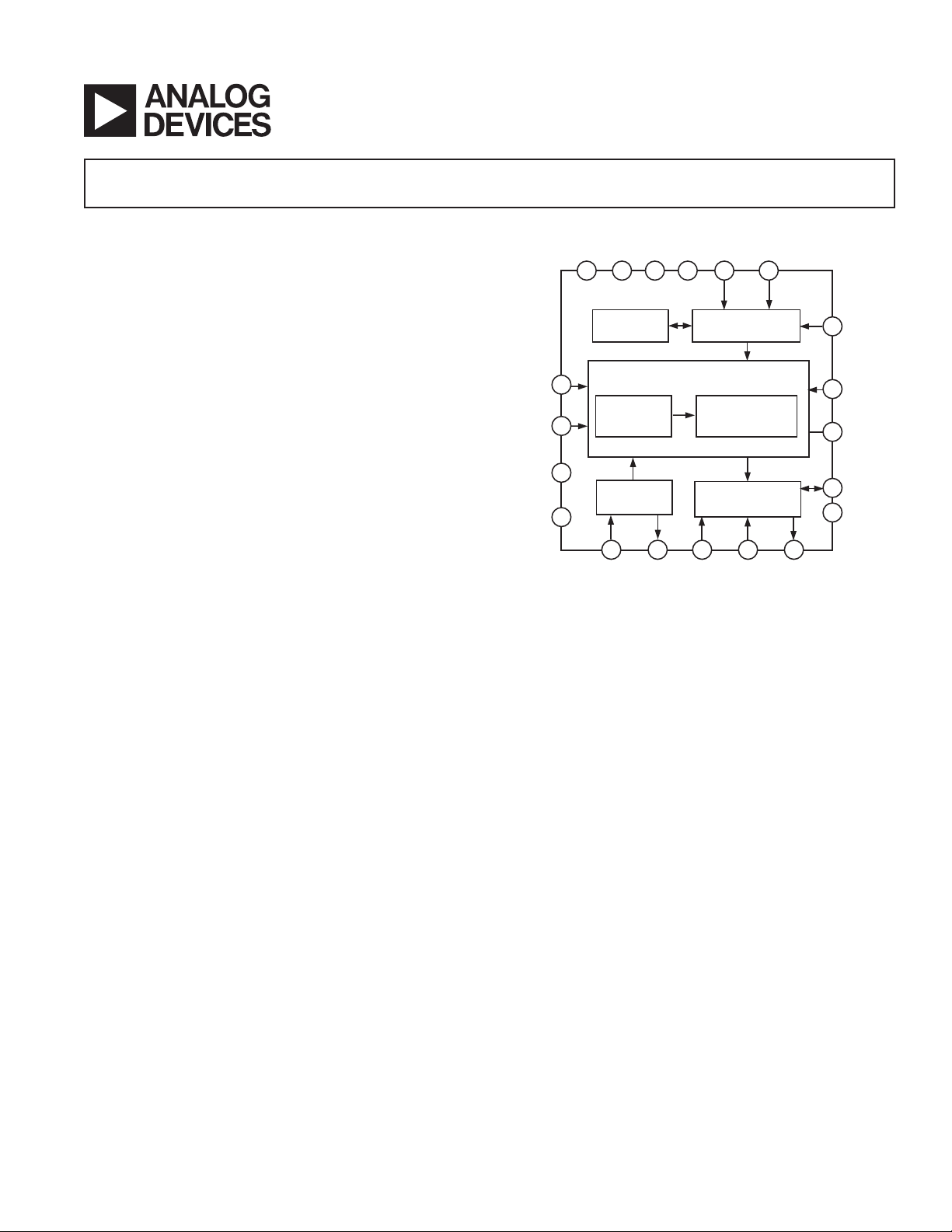
GENERAL DESCRIPTION
The AD7701 is a 16-bit ADC that uses a sigma-delta conversion
technique. The analog input is continuously sampled by an analog
modulator whose mean output duty cycle is proportional to the
input signal. The modulator output is processed by an on-chip
digital filter with a six-pole Gaussian response, which updates
the output data register with 16-bit binary words at word rates up
to 4 kHz. The sampling rate, filter corner frequency, and output
word rate are set by a master clock input that may be supplied
externally, or by a crystal controlled on-chip clock oscillator.
The inherent linearity of the ADC is excellent and endpoint
accuracy is ensured by self-calibration of zero and full scale,
which may be initiated at any time. The self-calibration scheme
can also be extended to null system offset and gain errors in the
input channel.
The output data is accessed through a flexible serial port, which
has an asynchronous mode compatible with UARTs and two
synchronous modes suitable for interfacing to shift registers or
the serial ports of industry-standard microcontrollers.
CMOS construction ensures low power dissipation, and a powerdown mode reduces the idle power consumption to only 10 µW.
FUNCTIONAL BLOCK DIAGRAM
PRODUCT HIGHLIGHTS
1. The AD7701 offers 16-bit resolution coupled with outstanding 0.0015% accuracy.
2. No missing codes ensures true, usable, 16-bit dynamic range,
removing the need for programmable gain and level-setting
circuitry.
3. The effects of temperature drift are eliminated by on-chip
self-calibration, which removes zero and gain error. External
circuits can also be included in the calibration loop to remove
system offsets and gain errors.
4. A flexible synchronous/asynchronous interface allows the
AD7701 to interface directly to UARTs or to the serial ports
of industry-standard microcontrollers.
5. Low operating power consumption and an ultralow power
standby mode make the AD7701 ideal for loop-powered
remote sensing applications, or battery-powered portable
instruments.
REV. E
Information furnished by Analog Devices is believed to be accurate and
reliable. However, no responsibility is assumed by Analog Devices for its
use, nor for any infringements of patents or other rights of third parties that
may result from its use. No license is granted by implication or otherwise
under any patent or patent rights of Analog Devices. Trademarks and
registered trademarks are the property of their respective companies.
One Technology Way, P.O. Box 9106, Norwood, MA 02062-9106, U.S.A.
Tel: 781/329-4700 www.analog.com
Fax: 781/326-8703 © 2003 Analog Devices, Inc. All rights reserved.

AD7701–SPECIFICATIONS
(TA = 25C; AVDD = DVDD = +5 V; AVSS = DVSS = –5 V; V
= +2.5 V; f
REF
= 4.096 MHz;
CLKIN
Bipolar Mode: MODE = +5 V; AIN Source Resistance = 1k1 with 1 nF to AGND at AIN; unless otherwise noted.)
Parameter A, S Version
2
B, T Version
STATIC PERFORMANCE
Resolution 16 16 Bits
Integral Nonlinearity
T
MIN
to T
MAX
±0.0007 % FSR typ
±0.003 ±0.0015 % FSR max
Differential Nonlinearity
T
to T
MIN
MAX
Positive Full-Scale Error
Full-Scale Drift
Unipolar Offset Error
Unipolar Offset Drift
Bipolar Zero Error
Bipolar Zero Drift
4
3
4
3
4
3
±0.125 ±0.125 LSB typ Guaranteed No Missing Codes
±0.5 ±0.5 LSB max
±0.13 ±0.13 LSB typ
±0.5 ±0.5 LSB max
±1.2 (±2.3 S Version) ±1.2 (±2.3 T Version) LSB typ
±0.25 ±0.25 LSB typ
±1 ±1 LSB max
±1.6 (+3/–25 S Version) ±1.6 (+3/–25 T Version) LSB typ
±0.25 ±0.25 LSB typ
±1 ± 1 LSB max
±0.8 (+1.5/–12.5 S Version) ±0.8 (+1.5/–12.5 T Version) LSB typ
Bipolar Negative Full-Scale Error3±0.5 ±0.5 LSB typ
±2 ±2 LSB max
Bipolar Negative Full-Scale Drift4±0.6 (±1.2 S Version) ±0.6 (±1.2 T Version) LSB typ
Noise (Referred to Output) 0.1 0.1 LSB rms typ
DYNAMIC PERFORMANCE
Sampling Frequency, f
Output Update Rate, f
Filter Corner Frequency, f
S
OUT
–3 dB
Settling Time to ±0.0007% FS 507904/f
f
/256 f
CLKIN
f
/1024 f
CLKIN
f
/409,600 f
CLKIN
CLKIN
CLKIN
CLKIN
CLKIN
507904/f
SYSTEM CALIBRATION Applies to unipolar and
Positive Full-Scale Overrange V
Positive Full-Scale Overrange V
Negative Full-Scale Overrange –(V
Maximum Offset Calibration Range
5, 6
Unipolar Input Range –(V
Bipolar Input Range –0.4 V
Input Span
7
+ 0.1 V
REF
+ 0.1 V
REF
+ 0.1) –(V
REF
+ 0.1) –(V
REF
to +0.4 V
REF
0.8 V
REF
2 V
+ 0.2 2 V
REF
REF
+ 0.1 V max bipolar ranges. After cali-
REF
+ 0.1 V max bration, if AIN > V
REF
REF
REF
–0.4 V
0.8 V
REF
REF
ANALOG INPUT
Unipolar Input Range 0 to 2.5 0 to 2.5 V
Bipolar Input Range ±2.5 ±2.5 V
Input Capacitance 10 10 pF typ
Input Bias Current
1
11 nA typ
LOGIC INPUTS
All Inputs Except CLKIN
V
, Input Low Voltage 0.8 0.8 V max
INL
V
, Input High Voltage 2.0 2.0 V min
INH
CLKIN
V
, Input Low Voltage 0.8 0.8 V max
INL
V
, Input High Voltage 3.5 3.5 V min
INH
IIN, Input Current 10 10 µA max
LOGIC OUTPUTS
VOL, Output Low Voltage 0.4 0.4 V max I
VOH, Output High Voltage DVDD – 1 DVDD – 1 V min I
Floating State Leakage Current ±10 ±10 µA max
Floating State Output Capacitance 9 9 pF typ
2
Unit Test Conditions/Comments
/256 Hz
/1024 Hz
/409,600 Hz
CLKIN
sec For Full-Scale Input Step
, the
REF
+ 0.1) V max device will output all 1s.
If AIN < 0 (unipolar) or
+ 0.1) V max –V
to +0.4 V
REF
REF
V max will output all 0s.
(bipolar), the device
REF
V min
+ 0.2 V max
= 1.6 mA
SINK
= 100 µA
SOURCE
REV. E–2–

AD7701
Parameter A, S Version
POWER REQUIREMENTS
8
2
B, T Version
2
Unit Test Conditions/Comments
Power Supply Voltages
Analog Positive Supply (AV
Digital Positive Supply (DV
) 4.5/5.5 4.5/5.5 V min/V max
DD
) 4.5/AV
DD
DD
4.5/AV
DD
V min/V max
Analog Negative Supply (AVSS) –4.5/–5.5 –4.5/–5.5 V min/V max
Digital Negative Supply (DVSS) –4.5/–5.5 –4.5/–5.5 V min/V max
Calibration Memory Retention
Power Supply Voltage 2.0 2.0 V min
DC Power Supply Currents
8
Analog Positive Supply (AIDD) 2.7 2.7 mA max Typically 2 mA
Digital Positive Supply (DI
Analog Negative Supply (AI
Digital Negative Supply (DI
Power Supply Rejection
)2 2 mA max Typically 1 mA
DD
) 2.7 2.7 mA max Typically 2 mA
SS
) 0.1 0.1 mA max Typically 0.03 mA
SS
9
Positive Supplies 70 70 dB typ
Negative Supplies 75 75 dB typ
Power Dissipation
Normal Operation 37 37 mW max SLEEP = Logic 1,
Typically 25 mW
Standby Operation
10
20 (40 S Version) 20 (40 T Version) µW max SLEEP = Logic 0,
Typically 10 µW
NOTES
1
The AIN pin presents a very high impedance dynamic load that varies with clock frequency.
2
Temperature ranges are as follows: A, B Versions: –40°C to +85°C; S, T Versions: –55°C to +125°C.
3
Apply after calibration at the temperature of interest. Full-scale error applies for both unipolar and bipolar input ranges.
4
Total drift over the specified temperature range since calibration at power-up at 25 °C. This is guaranteed by design and/or characterization. Recalibration at
any temperature will remove these errors.
5
In Unipolar mode, the offset can have a negative value (–V
6
The specifications for input overrange and for input span apply additional constraints on the offset calibration range.
7
For Unipolar mode, input span is the difference between full scale and zero scale. For Bipolar mode, input span is the difference between positive and
negative full-scale points. When using less than the maximum input span, the span range may be placed anywhere within the range of ±(V
8
All digital outputs unloaded. All digital inputs at 5 V CMOS levels.
9
Applies in 0.1 Hz to 10 Hz bandwidth. PSRR at 60 Hz will exceed 120 dB due to the digital filter.
10
CLKIN is stopped. All digital inputs are grounded.
) such that the Unipolar mode can mimic Bipolar mode operation.
REF
REF
+0.1).
Specifications subject to change without notice.
REV. E
–3–
AD7701
ABSOLUTE MAXIMUM RATINGS
1
(TA = 25°C, unless otherwise noted.)
DVDD to AGND . . . . . . . . . . . . . . . . . . . . . . . –0.3 V to +6 V
to AVDD . . . . . . . . . . . . . . . . . . . . . . . –0.3 V to +0.3 V
DV
DD
DV
to AGND . . . . . . . . . . . . . . . . . . . . . . . . +0.3 V to –6 V
SS
AV
to AGND . . . . . . . . . . . . . . . . . . . . . . . –0.3 V to +6 V
DD
to AGND . . . . . . . . . . . . . . . . . . . . . . . . +0.3 V to –6 V
AV
SS
AGND to DGND . . . . . . . . . . . . . . . . . . . . . –0.3 V to +0.3 V
Digital Input Voltage to DGND . . . . –0.3 V to DV
+ 0.3 V
DD
Analog Input
Voltage to AGND . . . . . . . . AV
Input Current to Any Pin Except Supplies
– 0.3 V to AVDD + 0.3 V
SS
2
. . . . . . . . ± 10 mA
ORDERING GUIDE
Temperature Linearity Package
Model Range Error (% FSR) Options*
AD7701AN –40°C to +85°C 0.003 N-20
AD7701BN –40°C to +85°C 0.0015 N-20
AD7701AR –40°C to +85°C 0.003 R-20
AD7701BR –40°C to +85°C 0.0015 R-20
AD7701ARS –40°C to +85°C 0.003 RS-28
AD7701AQ –40°C to +85°C 0.003 Q-20
AD7701BQ –40°C to +85°C 0.0015 Q-20
AD7701SQ –55°C to +125°C 0.003 Q-20
AD7701TQ –55°C to +125°C 0.0015 Q-20
*N = PDIP; Q = CERDIP; R = SOIC; RS = SSOP.
Operating Temperature Range
Commercial Plastic (A, B Versions) . . . . . –40°C to +85°C
Industrial CERDIP (A, B Versions) . . . . . . –40°C to +85°C
Extended CERDIP (S, T Versions) . . . . . –55°C to +125°C
Storage Temperature Range. . . . . . . . . . . . . –65°C to +150°C
Lead Temperature (Soldering, 10 secs) . . . . . . . . . . . . . 300°C
Power Dissipation (Any Package) to 75°C . . . . . . . . . 450 mW
Derates above 75°C by . . . . . . . . . . . . . . . . . . . . . 10 mW/°C
NOTES
1
Stresses above those listed under Absolute Maximum Ratings may cause perma-
nent damage to the device. This is a stress rating only; functional operation of the
device at these or any other conditions above those listed in the operational
sections of this specification is not implied. Exposure to absolute maximum rating
conditions for extended periods may affect device reliability.
2
Transient currents of up to 100 mA will not cause SCR latch-up.
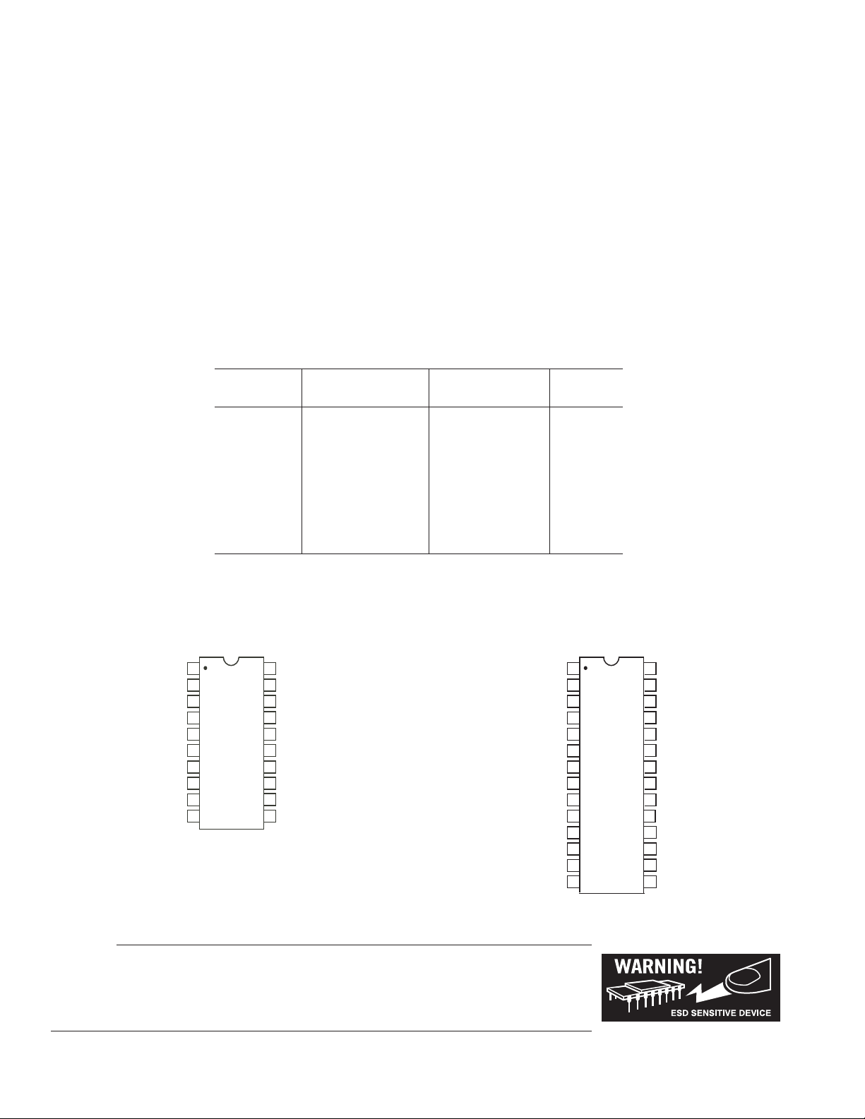
PIN CONFIGURATIONS
PDIP, CERDIP, SOIC
MODE
CLKOUT
CLKIN
SC1
DGND
DV
AV
AGND
A
V
REF
SS
SS
IN
1
2
3
4
AD7701
5
TOP VIEW
(Not to Scale)
6
7
8
9
10
20
19
18
17
16
15
14
13
12
11
SDATA
SCLK
DRDY
SC2
CS
DV
DD
AV
DD
CAL
BP/UP
SLEEP
MODE
CLKOUT
CLKIN
SC1
DGND
DV
AV
AGND
V
SSOP
1
2
3
4
5
6
NC
AD7701
NC
7
TOP VIEW
8
SS
(Not to Scale)
NC
9
10
SS
NC
11
12
A
13
IN
REF
14
NC = NO CONNECT
CAUTION
ESD (electrostatic discharge) sensitive device. Electrostatic charges as high as 4000 V readily
accumulate on the human body and test equipment and can discharge without detection. Although the
AD7701 features proprietary ESD protection circuitry, permanent damage may occur on devices
subjected to high energy electrostatic discharges. Therefore, proper ESD precautions are recommended
to avoid performance degradation or loss of functionality.
28
27
26
25
24
23
22
21
20
19
18
17
16
15
SDATA
SCLK
DRDY
SC2
CS
NC
NC
NC
DV
DD
AV
DD
NC
CAL
BP/UP
SLEEP
REV. E–4–

AD7701
PIN FUNCTION DESCRIPTIONS
Pin No.
PDIP,
CERDIP,
SOIC SSOP Mnemonic Description
11 MODE Selects the Serial Interface Mode. If MODE is tied to –5 V, the AD7701 will operate in
the Asynchronous Communications (AC) mode. The SCLK pin is configured as an
input, and data is transmitted in two bytes, each with one start bit and two stop bits. If
MODE is tied to DGND, the Synchronous External Clocking (SEC) mode is selected.
SCLK is configured as an input, and the output appears without formatting, the MSB
coming first. If MODE is tied to +5 V, the AD7701 operates in the Synchronous
Self-Clocking (SSC) mode. SCLK is configured as an output, with a clock frequency of
/4 and 25% duty cycle.
f
CLKlN
22 CLKOUT Clock Output to Generate an Internal Master Clock by Connecting a Crystal between
CLKOUT and CLKIN. If an external clock is used, CLKOUT is not connected.
33 CLKIN Clock Input for External Clock.
4, 17 4, 25 SC1, SC2 System Calibration Pins. The state of these pins, when CAL is taken high, determines
the type of calibration performed.
55 DGND Digital Ground. Ground reference for all digital signals.
68 DV
SS
6, 7, 9, 11, NC No Connect.
18, 21, 22, 23
710 AV
SS
812 AGND Analog Ground. Ground reference for all analog signals.
913 A
10 14 V
IN
REF
11 15 SLEEP Sleep Mode Pin. When this pin is taken low, the AD7701 goes into a low power mode
12 16 BP/UP Bipolar/Unipolar Mode Pin. When this pin is low, the AD7701 is configured for a uni-
13 17 CAL Calibration Mode Pin. When CAL is taken high for more than four cycles, the AD7701
14 19 AV
15 20 DV
DD
DD
16 24 CS Chip Select Input. When CS is brought low, the AD7701 will begin to transmit serial
18 26 DRDY Data Ready Output. DRDY is low when valid data is available in the output register. It
19 27 SCLK Serial Clock Input/Output. The SCLK pin is configured as an input or output, depen-
20 28 SDATA Serial Data Output. The AD7701’s output data is available at this pin as a 16-bit serial
Digital Negative Supply, –5 V Nominal.
Analog Negative Supply, –5 V Nominal.
Analog Input.
Voltage Reference Input, 2.5 V Nominal. This determines the value of positive full scale
in the Unipolar mode and of both positive and negative full scale in Bipolar mode.
with typically 10 µW power consumption.
polar input range going from AGND to V
configured for a bipolar input range, ±V
. When Pin 12 is high, the AD7701 is
REF
.
REF
is reset and performs a calibration cycle when CAL is brought low again. The CAL pin
can also be used as a strobe to synchronize the operation of several AD7701s.
Analog Positive Supply, +5 V Nominal.
Digital Positive Supply, +5 V Nominal.
data in a format determined by the state of the MODE pin.
goes high after transmission of a word is completed. It also goes high for four clock
cycles when a new data-word is being loaded into the output register, to indicate that
valid data is not available, irrespective of whether data transmission is complete or not.
dent on the type of serial data transmission that has been selected by the MODE pin.
When configured as an output in the Synchronous Self-Clocking mode, it has a frequency of f
/4 and a duty cycle of 25%.
CLKIN
word. The transmission format is determined by the state of the MODE pin.
REV. E
–5–

AD7701
TIMING CHARACTERISTICS
Limit at T
MIN
, T
MAX
Limit at T
(AVDD = DVDD = +5 V 10%; AVSS = DVSS = –5 V 10%; AGND = DGND = O V; f
1, 2
4.096 MHz; Input Levels: Logic O = O V, Logic 1 = DV
, T
MIN
MAX
; unless otherwise noted.)
DD
CLKIN
=
Parameter (A, B Versions) (S, T Versions) Unit Conditions/Comments
3, 4
f
CLKIN
200 200 kHz min Master Clock Frequency: Internal Gate Oscillator.
55 MHz max Typically 4.096 MHz.
200 200 kHz min Master Clock Frequency: Externally Supplied.
5
t
r
5
t
f
t
1
t
2
6
t
3
SSC MODE
7
t
4
t
5
t
6
t
7
t
8
8
t
9
8, 9
t
10
55 MHz max
50 50 ns max Digital Output Rise Time. Typically 20 ns.
50 50 ns max Digital Output Fall Time. Typically 20 ns.
00 ns min SC1, SC2 to CAL High Setup Time.
50 50 ns min SC1, SC2 Hold Time after CAL Goes High.
1000 1000 ns min SLEEP High to CLKIN High Setup Time.
3/f
CLKIN
3/f
CLKIN
ns max Data Access Time (CS Low to Data Valid).
100 100 ns max SCLK Falling Edge to Data Valid Delay (25 ns typ).
250 250 ns min MSB Data Setup Time. Typically 380 ns.
300 300 ns max SCLK High Pulsewidth. Typically 240 ns.
790 790 ns max SCLK Low Pulsewidth. Typically 730 ns.
l/f
+200 l/f
CLKIN
(4/f
) +200 (4/f
CLKIN
+200 ns max SCLK Rising Edge to Hi-Z Delay (l/f
CLKIN
) +200 ns max CS High to Hi-Z Delay.
CLKIN
+ 100 ns typ).
CLKIN
SEC MODE
f
SCLK
t
11
t
12
t
13
t
14
t
15
t
16
7, 10
11
8
8
55 MHz Serial Clock Input Frequency.
35 35 ns min SCLK Input High Pulsewidth.
160 160 ns min SCLK Low Pulsewidth.
160 160 ns max Data Access Time (CS Low to Data Valid). Typically 80 ns.
150 150 ns max SCLK Falling Edge to Data Valid Delay. Typically 75 ns.
250 250 ns max CS High to Hi-Z Delay.
200 200 ns max SCLK Falling Edge to Hi-Z Delay. Typically 100 ns.
AC MODE
t
17
t
18
t
19
NOTES
1
Sample tested at 25°C to ensure compliance. All input signals are specified with tr = tf = 5 ns (10% to 90% of 5 V) and timed from a voltage level of 1.6 V.
2
See Figures 1 to 6.
3
CLKIN duty cycle range is 20% to 80%. CLKIN must be supplied whenever the AD7701 is not in SLEEP mode. If no clock is present in this case, the device can
draw higher current than specified and possibly become uncalibrated.
4
The AD7701 is production tested with f
5
Specified using 10% and 90% points on waveform of interest.
6
In order to synchronize several AD7701s together using the SLEEP pin, this specification must be met.
7
t4 and t13 are measured with the load circuit of Figure 1 and defined as the time required for an output to cross 0.8 V or 2.4 V.
8
t9, t10, t15, and t16 are derived from the measured time taken by the data outputs to change 0.5 V when loaded with the circuit of Figure 1. The measured number
is then extrapolated back to remove the effects of charging or discharging the 100 pF capacitor. This means that the time quoted in the Timing Characteristics is
the true bus relinquish time of the part and as such is independent of external bus loading capacitance.
9
If CS is returned high before all 16 bits are output, the SDATA and SCLK outputs will complete the current data bit and then go to high impedance.
10
If CS is activated asynchronously to DRDY , CS will not be recognized if it occurs when DRDY is high for four clock cycles. The propagation delay time may be
as great as four CLKIN cycles plus 160 ns. To guarantee proper clocking of SDATA when using asynchronous CS, the SCLK input should not be taken high
sooner than four CLKIN cycles plus 160 ns after CS goes low.
11
SDATA is clocked out on the falling edge of the SCLK input.
Specifications subject to change without notice.
40 40 ns min CS Setup Time. Typically 20 ns.
180 180 ns max Data Delay Time. Typically 90 ns.
200 200 ns max SCLK Falling Edge to Hi-Z Delay. Typically 100 ns.
at 4.096 MHz. It is guaranteed by characterization to operate at 200 kHz.
CLKIN
REV. E–6–
 Loading...