ANALOG DEVICES AD7691 Service Manual
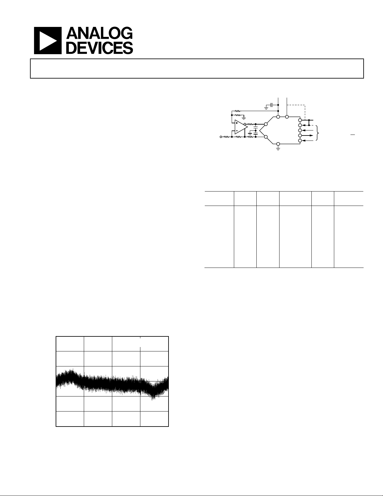
18-Bit, 1.5 LSB INL, 250 kSPS PulSAR
V
Data Sheet
FEATURES
18-bit resolution with no missing codes
Throughput: 250 kSPS
INL: ±0.75 LSB typical, ±1.5 LSB maximum (±6 ppm of FSR)
Dynamic range: 102 dB typical @ 250 kSPS
Oversampled dynamic range: 125 dB @1 kSPS
Noise-free code resolution: 20 bits @ 1 kSPS
Effective resolution: 22.7 bits @ 1 kSPS
SINAD: 101.5 dB typical @ 1 kHz
THD: −125 dB typical @ 1 kHz
True differential analog input range: ±V
0 V to V
with V
REF
up to VDD on both inputs
REF
No pipeline delay
Single-supply 2.3 V to 5 V operation with
1.8 V/2.5 V/3 V/5 V logic interface
Serial interface SPI-/QSPI™-/MICROWIRE™-/DSP-compatible
Ability to daisy-chain multiple ADCs
Optional busy indicator feature
Power dissipation
1.35 mW @ 2.5 V/100 kSPS, 4 mW @ 5 V/100 kSPS
1.4 μW @ 2.5 V/100 SPS
Standby current: 1 nA
10-lead packages: MSOP (MSOP-8 size) and
3 mm × 3 mm QFN (LFCSP) (SOT-23 size)
Pin-for-pin compatible with the18-bit AD7690 and
16-bit AD7693, AD7688, and AD7687
APPLICATIONS
Battery-powered equipment
Data acquisitions
Seismic data acquisition systems
Instrumentation
Medical instruments
1.5
1.0
0.5
0
INL (LSB)
–0.5
–1.0
–1.5
0 262144
Rev. C
Information furnished by Analog Devices is believed to be accurate and reliable. However, no
responsibility is assumed by Anal og Devices for its use, nor for any infringements of patents or ot her
rights of third parties that may result from its use. Specifications subject to change without notice. No
license is granted by implication or otherwise under any patent or patent rights of Analog Devices.
Trademarks and registered trademarks are the property of their respective owners.
65536 131072 196608
CODE
Figure 1. Integral Nonlinearity vs. Code, 5 V
REF
POSIT IVE INL = 0.43LSB
NEGATIVE INL = –0. 62LSB
06146-025
Differential ADC in MSOP/QFN
AD7691
APPLICATION DIAGRAM
+0.5V TO VDD
±10V, ±5V, ...
ADA4941
Table 1. MSOP, QFN (LFCSP)/SOT-23
14-/16-/18-Bit PulSAR® ADC
Type
18-Bit True
Differential
16-Bit True
Differential
16-Bit
Pseudo
Differential
14-Bit
Pseudo
Differential
100
kSPS
AD7691 AD7690
AD7684 AD7687 AD7688
AD7680
AD7683
AD7940 AD7942 AD7946 ADA4841-1
250
kSPS
AD7685
AD7694
GENERAL DESCRIPTION
The AD7691 is an 18-bit, charge redistribution, successive
approximation, analog-to-digital converter (ADC) that operates
from a single power supply, VDD, between 2.3 V and 5 V. It
contains a low power, high speed, 18-bit sampling ADC with no
missing codes, an internal conversion clock, and a versatile
serial interface port. On the CNV rising edge, it samples the
voltage difference between the IN+ and IN− pins. The voltages
on these pins swing in opposite phases between 0 V and REF.
The reference voltage, REF, is applied externally and can be set
up to the supply voltage.
The part’s power scales linearly with throughput.
The SPI-compatible serial interface also features the ability,
using the SDI input, to daisy-chain several ADCs on a single
3-wire bus and provides an optional busy indicator. It is compatible
with 1.8 V, 2.5 V, 3 V, or 5 V logic, using the separate VIO supply.
The AD7691 is housed in a 10-lead MSOP or a 10-lead QFN
(LFCSP) with operation specified from −40°C to +85°C.
One Technology Way, P.O. Box 9106, Norwood, MA 02062-9106, U.S.A.
Tel: 781.329.4700 www.analog.com
Fax: 781.461.3113 ©2006–2012 Analog Devices, Inc. All rights reserved.
+2.5V TO +5
IN+
IN–
SDI
SCK
SDO
GND
CNV
AD7691
Figure 2.
400 kSPS to
500 kSPS
AD7693
AD7686 AD7980 ADA4841-x
VIO
REF
VDD
+1.8V TO VDD
3- OR 4-WIRE
INTERFACE
(SPI, DAISY CHAIN, CS)
≥1000
kSPS
AD7982
AD7984
ADA4941-1
ADC
Driver
ADA4941-1
ADA4841-x
ADA4841-x
6146-001

AD7691 Data Sheet
TABLE OF CONTENTS
Features.............................................................................................. 1
Applications....................................................................................... 1
Application Diagram........................................................................ 1
General Description......................................................................... 1
Revision History ...............................................................................2
Specifications..................................................................................... 3
Timing Specifications ..................................................................5
Absolute Maximum Ratings............................................................ 7
Thermal Resistance...................................................................... 7
ESD Caution.................................................................................. 7
Pin Configurations and Function Descriptions........................... 8
Typical Performance Characteristics............................................. 9
Terminology.................................................................................... 13
Theory of Operation ......................................................................14
Circuit Information.................................................................... 14
Converter Operation.................................................................. 14
Typical Connection Diagram ...................................................15
Analog Inputs..............................................................................15
Driver Amplifier Choice ........................................................... 16
Single-to-Differential Driver ....................................................16
Voltage Reference Input ............................................................ 16
Power Supply............................................................................... 17
Supplying the ADC from the Reference.................................. 17
Digital Interface.......................................................................... 17
CS
Mode, 3-Wire Without Busy Indicator ............................. 18
CS
Mode, 3-Wire with Busy Indicator.................................... 19
CS
Mode, 4-Wire Without Busy Indicator ............................. 20
CS
Mode, 4-Wire with Busy Indicator.................................... 21
Chain Mode Without Busy Indicator...................................... 22
Chain Mode with Busy Indicator............................................. 23
Application Hints ...........................................................................24
Layout .......................................................................................... 24
Evaluating the AD7691 Performance...................................... 24
Outline Dimensions....................................................................... 25
Ordering Guide .......................................................................... 25
REVISION HISTORY
3/12—Rev. B to Rev. C
Change to Table 9........................................................................... 14
Changes to Ordering Guide.......................................................... 25
7/11—Rev. A to Rev. B
Changes to Common-Mode Input Range Min Parameter ......... 3
Added EPAD Note to Figure 6 and Table 8................................... 8
Updated Outline Dimensions....................................................... 25
11/07—Rev. 0 to Rev. A
Deleted QFN Package in Development References.......Universal
Changes to Features, Applications, Figure 1 and Figure 2.......... 1
Changes to Accuracy, Table 2.......................................................... 3
Changes to Power Dissipation, Table 3.......................................... 4
Added Thermal Resistance Section ............................................... 7
Changes to Figure 22...................................................................... 11
Changes to Format......................................................................... 12
Changes to Terminology Section.................................................. 13
Changes to Format and Figure 29 ................................................15
Inserted Figure 31........................................................................... 15
Changes to Format......................................................................... 17
Changes to Figure 44...................................................................... 22
Changes to Figure 46...................................................................... 23
Updated QFN Outline Dimensions............................................. 25
Changes to Ordering Guide.......................................................... 25
7/06—Revision 0: Initial Version
Rev. C | Page 2 of 28

Data Sheet AD7691
SPECIFICATIONS
VDD = 2.3 V to 5.25 V, VIO = 2.3 V to VDD, V
Table 2.
Parameter Conditions/Comments Min Typ Max Unit
RESOLUTION 18 Bits
ANALOG INPUT
Voltage Range, V
IN
Absolute Input Voltage IN+, IN− −0.1 V
Common-Mode Input Range IN+, IN− V
Analog Input CMRR fIN = 250 kHz 65 dB
Leakage Current at 25°C Acquisition phase 1 nA
Input Impedance1
THROUGHPUT
Conversion Rate VDD = 4.5 V to 5.25 V 0 250 kSPS
VDD = 2.3 V to 4.5 V 0 180 kSPS
Transient Response Full-scale step 1.8 s
ACCURACY
No Missing Codes 18 Bits
Integral Linearity Error −1.5 ±0.75 +1.5 LSB2
Differential Linearity Error −1 ±0.5 +1.25 LSB2
Transition Noise REF = VDD = 5 V 0.75 LSB2
Gain Error3 VDD = 4.5 V to 5.25 V −40 ±2 +40 LSB2
VDD = 2.3 V to 4.5 V −80 ±2 +80 LSB2
Gain Error Temperature Drift ±0.3 ppm/°C
Zero Error3 VDD = 4.5 V to 5.25 V −0.8 ±0.1 +0.8 mV
VDD = 2.3 V to 4.5 V −3.5 ±0.7 +3.5 mV
Zero Temperature Drift ±0.3 ppm/°C
Power Supply Sensitivity
AC ACCURACY4
Dynamic Range V
Oversampled Dynamic Range5 f
Signal-to-Noise fIN = 1 kHz, V
f
Spurious-Free Dynamic Range fIN = 1 kHz, V
Total Harmonic Distortion fIN = 1 kHz, V
Signal-to-(Noise + Distortion) fIN = 1 kHz, V
f
Intermodulation Distortion6 115 dB
1
See the Analog Inputs section.
2
LSB means least significant bit. With the ±5 V input range, one LSB is 38.15 µV.
3
See the Terminology section. These specifications include full temperature range variation but not the error contribution from the external reference.
4
All ac accuracy specifications in dB are referred to a full-scale input FSR. Tested with an input signal at 0.5 dB below full scale, unless otherwise specified.
5
Dynamic range obtained by oversampling the ADC running at a throughput fS of 250 kSPS, followed by postdigital filtering with an output word rate fO.
6
f
= 21.4 kHz and f
IN1
= 18.9 kHz, with each tone at −7 dB below full scale.
IN2
= VDD, all specifications T
REF
IN+ − (IN−) −V
VDD = 5 V ± 5%
= 5 V 101 102 dB
REF
= 1 kSPS 125 dB
IN
= 5 V 100 101.5 dB
REF
= 1 kHz, V
IN
= 1 kHz, V
IN
= 2.5 V 95 96.5 dB
REF
= 5 V −125 dB
REF
= 5 V −118 dB
REF
= 5 V 100 101.5 dB
REF
= 2.5 V 95 96.5 dB
REF
MIN
to T
, unless otherwise noted.
MAX
+V
REF
/2 − 0.1 V
REF
/2 V
REF
REF
+ 0.1 V
REF
/2 + 0.1 V
REF
±0.25 LSB2
V
Rev. C | Page 3 of 28

AD7691 Data Sheet
VDD = 2.3 V to 5.25 V, VIO = 2.3 V to VDD, V
Table 3.
Parameter Conditions/Comments Min Typ Max Unit
REFERENCE
Voltage Range 0.5 VDD + 0.3 V
Load Current 250 kSPS, REF = 5 V 60 µA
SAMPLING DYNAMICS
−3 dB Input Bandwidth 2 MHz
Aperture Delay VDD = 5 V 2.5 ns
DIGITAL INPUTS
Logic Levels
VIL −0.3 +0.3 × VIO V
VIH 0.7 × VIO VIO + 0.3 V
IIL −1 +1 µA
IIH −1 +1 µA
DIGITAL OUTPUTS
Data Format Serial 18-bit, twos complement
Pipeline Delay1
VOL I
VOH I
= +500 µA 0.4 V
SINK
= −500 µA VIO − 0.3 V
SOURCE
POWER SUPPLIES
VDD Specified performance 2.3 5.25 V
VIO Specified performance 2.3 VDD + 0.3 V
VIO Range 1.8 VDD + 0.3 V
Standby Current
2, 3
VDD and VIO = 5 V, TA = 25°C 1 50 nA
Power Dissipation VDD = 2.5 V, 100 SPS throughput 1.4 µW
VDD = 2.5 V, 100 kSPS throughput 1.35 mW
VDD = 2.5 V, 180 kSPS throughput 2.4 mW
VDD = 5 V, 100 kSPS throughput 4.24 5 mW
VDD = 5 V, 250 kSPS throughput 10.6 12.5 mW
Energy per Conversion 50 nJ/sample
TEMPERATURE RANGE4
Specified Performance T
1
Conversion results are available immediately after completed conversion.
2
With all digital inputs forced to VIO or GND as required.
3
During acquisition phase.
4
Contact an Analog Devices, Inc., sales representative for the extended temperature range.
MIN
to T
= VDD, all specifications T
REF
−40 +85 °C
MAX
MIN
to T
, unless otherwise noted.
MAX
Rev. C | Page 4 of 28
Data Sheet AD7691
TIMING SPECIFICATIONS
VDD = 4.5 V to 5.25 V, VIO = 2.3 V to VDD, V
Table 4.
Parameter Symbol Min Typ Max Unit
Conversion Time: CNV Rising Edge to Data Available t
Acquisition Time t
Time Between Conversions t
CNV Pulse Width (CS Mode)
SCK Period (CS Mode)
SCK Period (Chain Mode) t
VIO Above 4.5 V 17 ns
VIO Above 3 V 18 ns
VIO Above 2.7 V 19 ns
VIO Above 2.3 V 20 ns
SCK Low Time t
SCK High Time t
SCK Falling Edge to Data Remains Valid t
SCK Falling Edge to Data Valid Delay t
VIO Above 4.5 V 14 ns
VIO Above 3 V 15 ns
VIO Above 2.7 V 16 ns
VIO Above 2.3 V 17 ns
CNV or SDI Low to SDO D17 MSB Valid (CS Mode)
VIO Above 4.5 V 15 ns
VIO Above 2.7 V 18 ns
VIO Above 2.3 V 22 ns
CNV or SDI High or Last SCK Falling Edge to SDO High Impedance (CS Mode)
SDI Valid Setup Time from CNV Rising Edge (CS Mode)
SDI Valid Hold Time from CNV Rising Edge (CS Mode)
SCK Valid Setup Time from CNV Rising Edge (Chain Mode) t
SCK Valid Hold Time from CNV Rising Edge (Chain Mode) t
SDI Valid Setup Time from SCK Falling Edge (Chain Mode) t
SDI Valid Hold Time from SCK Falling Edge (Chain Mode) t
SDI High to SDO High (Chain Mode with Busy Indicator) t
VIO Above 4.5 V 15 ns
VIO Above 2.3 V 26 ns
1
See Figure 3 and Figure 4 for load conditions.
= VDD, all specifications T
REF
to T
MIN
CONV
ACQ
CYC
t
CNVH
t
SCK
SCK
SCKL
SCKH
HSDO
DSDO
t
EN
t
25 ns
DIS
t
SSDICNV
t
HSDICNV
SSCKCNV
HSCKCNV
SSDISCK
HSDISCK
DSDOSDI
, unless otherwise noted.1
MAX
0.5 2.2 µs
1.8 µs
4 µs
10 ns
15 ns
7 ns
7 ns
4 ns
15 ns
0 ns
5 ns
10 ns
3 ns
4 ns
Rev. C | Page 5 of 28
AD7691 Data Sheet
VDD = 2.3 V to 4.5 V, VIO = 2.3 V to VDD, V
Table 5.
Parameter Symbol Min Typ Max Unit
Conversion Time: CNV Rising Edge to Data Available t
Acquisition Time t
Time Between Conversions t
CNV Pulse Width (CS Mode)
SCK Period (CS Mode)
SCK Period (Chain Mode) t
VIO Above 3 V 29 ns
VIO Above 2.7 V 35 ns
VIO Above 2.3 V 40 ns
SCK Low Time t
SCK High Time t
SCK Falling Edge to Data Remains Valid t
SCK Falling Edge to Data Valid Delay t
VIO Above 3 V 24 ns
VIO Above 2.7 V 30 ns
VIO Above 2.3 V 35 ns
CNV or SDI Low to SDO D17 MSB Valid (CS Mode)
VIO Above 2.7 V 18 ns
VIO Above 2.3 V 22 ns
CNV or SDI High or Last SCK Falling Edge to SDO High Impedance (CS Mode)
SDI Valid Setup Time from CNV Rising Edge (CS Mode)
SDI Valid Hold Time from CNV Rising Edge (CS Mode)
SCK Valid Setup Time from CNV Rising Edge (Chain Mode) t
SCK Valid Hold Time from CNV Rising Edge (Chain Mode) t
SDI Valid Setup Time from SCK Falling Edge (Chain Mode) t
SDI Valid Hold Time from SCK Falling Edge (Chain Mode) t
SDI High to SDO High (Chain Mode with Busy Indicator) t
1
See Figure 3 and Figure 4 for load conditions.
500µA I
TO SDO
50pF
C
L
500µA I
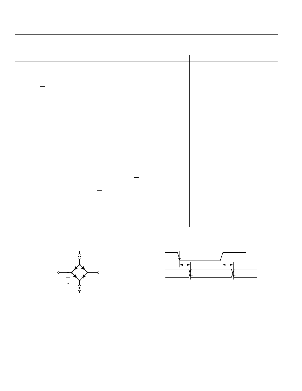
Figure 3. Load Circuit for Digital Interface Timing
OL
OH
= VDD, all specifications T
REF
1.4V
06146-002
MIN
CONV
ACQ
CYC
t
CNVH
t
SCK
SCK
SCKL
SCKH
HSDO
DSDO
t
EN
t
DIS
t
SSDICNV
t
HSDICNV
SSCKCNV
HSCKCNV
SSDISCK
HSDISCK
DSDOSDI
to T
, unless otherwise noted.1
MAX
0.5 3.7 µs
1.8 ns
5.5 µs
10 ns
25 ns
12 ns
12 ns
5 ns
25 ns
30 ns
0 ns
5 ns
8 ns
8 ns
10 ns
36
30% VIO
t
DELAY
2V OR VIO – 0.5V
0.8V OR 0.5V
1
2V IF VI O ABOVE 2. 5V, VIO – 0.5V IF VIO BEL OW 2.5V.
2
0.8V IF V IO ABOVE 2.5V, 0.5V IF VI O BELOW 2.5V.
Figure 4. Voltage Levels for Timing
70% VIO
t
1
2
DELAY
2V OR VIO – 0.5V
0.8V OR 0.5V
2
1
06146-003
Rev. C | Page 6 of 28
Data Sheet AD7691
ABSOLUTE MAXIMUM RATINGS
Table 6.
Parameter Rating
Analog Inputs (IN+, IN−)1
REF GND − 0.3 V to VDD + 0.3 V
Supply Voltages
VDD, VIO to GND −0.3 V to +7 V
VDD to VIO ±7 V
Digital Inputs to GND −0.3 V to VIO + 0.3 V
Digital Outputs to GND −0.3 V to VIO + 0.3 V
Storage Temperature Range −65°C to +150°C
Junction Temperature 150°C
Lead Temperature Range JEDEC J-STD-20
1
See the Analog Inputs section.
GND − 0.3 V to VDD + 0.3 V
or ±130 mA
Stresses above those listed under Absolute Maximum Ratings
may cause permanent damage to the device. This is a stress
rating only; functional operation of the device at these or any
other conditions above those indicated in the operational
section of this specification is not implied. Exposure to absolute
maximum rating conditions for extended periods may affect
device reliability.
THERMAL RESISTANCE
θJA is specified for the worst-case conditions, that is, a device
soldered in a circuit board for surface-mount packages.
Table 7. Thermal Resistance
Package Type θJA θJC Unit
10-Lead MSOP 200 44 °C/W
10-Lead QFN (LFCSP) 43.4 6.5 °C/W
ESD CAUTION
Rev. C | Page 7 of 28
AD7691 Data Sheet
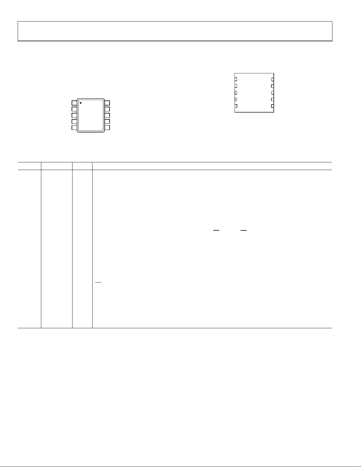
PIN CONFIGURATIONS AND FUNCTION DESCRIPTIONS
REF
VDD
IN+
IN–
GND
1
2
AD7691
3
TOP VIEW
(Not to Scale)
4
5
VIO
10
SDI
9
SCK
8
SDO
7
CNV
6
06146-004
Figure 5. 10-Lead MSOP Pin Configuration
Table 8. Pin Function Descriptions
Pin No. Mnemonic Type1 Description
1 REF AI
Reference Input Voltage. The REF range is from 0.5 V to VDD. It is referred to the GND pin.
This pin should be decoupled closely to the pin with a 10 µF capacitor.
2 VDD P Power Supply.
3 IN+ AI
4 IN− AI
5 GND P
6 CNV DI
Differential Positive Analog Input. Referenced to IN−. The input range for IN+ is between 0 V and V
centered about V
/2 and must be driven 180° out of phase with IN−.
REF
Differential Negative Analog Input. Referenced to IN+. The input range for IN− is between 0 V and V
centered about V
/2 and must be driven 180° out of phase with IN+.
REF
Power Supply Ground.
Convert Input. This input has multiple functions. On its leading edge, it initiates the conversions and
selects the interface mode of the part, either chain or CS
low. In chain mode, the data should be read when CNV is high.
7 SDO DO
8 SCK DI
9 SDI DI
Serial Data Output. The conversion result is output on this pin. It is synchronized to SCK.
Serial Data Clock Input. When the part is selected, the conversion result is shifted out by this clock.
Serial Data Input. This input provides multiple features. It selects the interface mode of the ADC as follows:
Chain mode is selected if SDI is low during the CNV rising edge. In this mode, SDI is used as a data input to
daisy-chain the conversion results of two or more ADCs onto a single SDO line. The digital data level on
SDI is output on SDO with a delay of 18 SCK cycles.
mode is selected if SDI is high during the CNV rising edge. In this mode, either SDI or CNV can enable
CS
the serial output signals when low, and if SDI or CNV is low when the conversion is complete, the busy
indicator feature is enabled.
10 VIO P
Input/Output Interface Digital Power. Nominally at the same supply as the host interface
(1.8 V, 2.5 V, 3 V, or 5 V ).
EPAD
Exposed Pad. The exposed pad is not connected internally. For increased reliability of the solder joints, it is
recommended that the pad be soldered to the ground plane.
1
AI = analog input, DI = digital input, DO = digital output, and P = power.
1REF
2VDD
AD7691
3IN+
TOP VIEW
4IN–
(Not to Scale)
5GND
NOTES
1. THE EXPOSED PAD IS NOT CONNECTED
INTERNALL Y. FO R INCREASED REL IABILI TY OF
THE SOL DER JOINTS , IT I S RECOMMENDED THAT
THE PAD BE SO LDERED TO THE GRO UND PLANE.
10 VI O
9SDI
8SCK
7SDO
6 CNV
Figure 6. 10-Lead QFN (LFCSP) Pin Configuration
mode. In CS mode, it enables the SDO pin when
06146-005
,
REF
,
REF
Rev. C | Page 8 of 28
Data Sheet AD7691
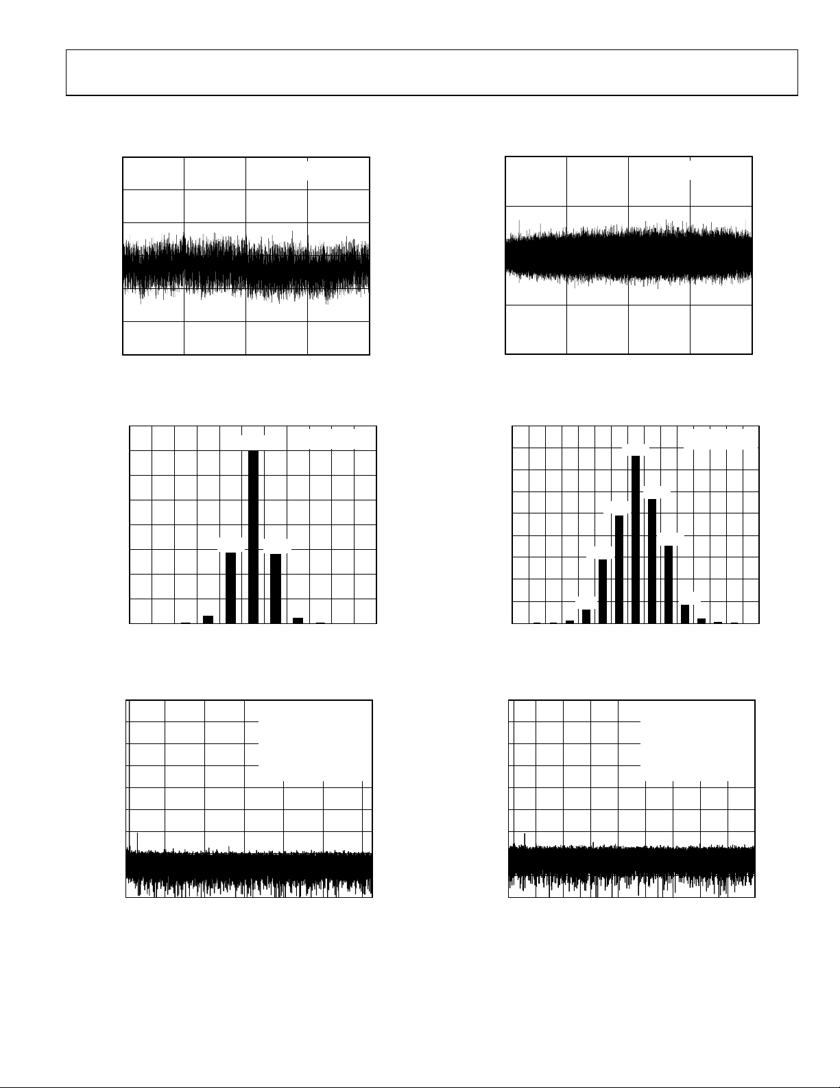
TYPICAL PERFORMANCE CHARACTERISTICS
1.5
1.0
0.5
0
INL (LSB)
–0.5
–1.0
–1.5
0 262144
65536 131072 196608
POSIT IVE INL = 0.39LSB
NEGATIVE INL = –0. 73LSB
CODE
Figure 7. Integral Nonlinearity vs. Code 2.5 V
80k
2904
69769
28527
CODE IN HEX
27770
70k
60k
50k
40k
COUNTS
30k
20k
10k
0
0
25
26
0
26 27 28 29 2A 2B 2C 2D 2E 2F
VDD = REF = 5V
σ = 0.76LSB
2062
14
Figure 8. Histogram of a DC Input at the Code Center, 5 V
1.0
0.5
0
DNL (LSB)
–0.5
–1.0
0 262144
06146-026
65536 131072 196608
POSITIVE DNL = 0. 37LSB
NEGATIVE DNL = –0.33L SB
CODE
06146-029
Figure 10. Differential Nonlinearity vs. Code, 5 V
45k
40k
35k
30k
25k
20k
COUNTS
15k
10k
5k
0
0
06146-027
01229
0
2423 25 26 28 29 2B2A 2C 2D 2F2E 30 31
2997
501
27
38068
24411
14362
CODE IN HEX
28179
17460
VDD = REF = 2.5V
σ = 1.42LSB
4055
910
78 9 0
06146-030
Figure 11. Histogram of a DC Input at the Code Center, 2.5 V
–100
–120
–140
AMPLITUDE (dB of Full Scal e)
–160
–180
–20
–40
–60
–80
0
0
20 40 60 80 100 120
FREQUENCY (kHz)
32768 POINT FFT
VDD = REF = 5V
f
= 250kSPS
S
f
= 2kHz
IN
SNR = 101.4dB
THD = –120.1dB
2ND HARMONIC = –140. 7dB
3RD HARMONIC = –120. 3dB
06146-028
Figure 9. 2 kHz FFT Plot, 5 V
AMPLITUDE (dB of Full Scal e)
–20
–40
–60
–80
–100
–120
–140
–160
–180
0
0
2010 30 40 50 60 70 80 90
FREQUENCY (kHz)
32768 POINT FFT
VDD = REF = 2.5V
f
= 180kSPS
S
f
= 2kHz
IN
SNR = 96.4dB
THD = –120.3dB
2ND HARMONIC = –132.5d B
3RD HARMONIC = –121.2d B
06146-031
Figure 12. 2 kHz FFT Plot, 2.5 V
Rev. C | Page 9 of 28
 Loading...