16-Bit, 30 MSPS
a
FEATURES
30 MSPS Update Rate
16-Bit Resolution
Linearity: 1/2 LSB DNL @ 14 Bits
1 LSB INL @ 14 Bits
Fast Settling: 25 ns Full-Scale Settling to 0.025%
SFDR @ 1 MHz Output: 86 dBc
THD @ 1 MHz Output: 71 dBc
Low Glitch Impulse: 35 pV-s
Power Dissipation: 465 mW
On-Chip 2.5 V Reference
Edge-Triggered Latches
Multiplying Reference Capability
APPLICATIONS
Arbitrary Waveform Generation
Communications Waveform Reconstruction
Vector Stroke Display
PRODUCT DESCRIPTION
The AD768 is a 16-bit, high speed digital-to-analog converter
(DAC) that offers exceptional ac and dc performance. The
AD768 is manufactured on ADI’s Advanced Bipolar CMOS
(ABCMOS) process, combining the speed of bipolar transistors,
the accuracy of laser-trimmable thin film resistors, and the efficiency of CMOS logic. A segmented current source architecture
is combined with a proprietary switching technique to reduce
glitch energy and maximize dynamic accuracy. Edge triggered
input latches and a temperature compensated bandgap reference
have been integrated to provide a complete monolithic DAC
solution.
The AD768 is a current-output DAC with a nominal full-scale
output current of 20 mA and a 1 kΩ output impedance. Differential current outputs are provided to support single-ended
or differential applications. The current outputs may be tied
directly to an output resistor to provide a voltage output, or fed
to the summing junction of a high speed amplifier to provide a
buffered voltage output. Also, the differential outputs may be
interfaced to a transformer or differential amplifier.
The on-chip reference and control amplifier are configured for
maximum accuracy and flexibility. The AD768 can be driven by
the on-chip reference or by a variety of external reference voltages based on the selection of an external resistor. An external
capacitor allows the user to optimally trade off reference bandwidth and noise performance.
The AD768 operates on ± 5 V supplies, typically consuming
465 mW of power. The AD768 is available in a 28-pin SOIC
package and is specified for operation over the industrial temperature range.
D/A Converter
AD768
FUNCTIONAL BLOCK DIAGRAM
V
DCOM
(MSB)
DB15
MSBs: SEGMENTED
CURRENT SOURCES
AND SWITCHES
MSB
DB0
(LSB)
DECODER
AND
EDGE-
TRIGGERED
BIT
LATCHES
CLOCK
LSBs:
CURRENT SOURCES,
SWITCHES, AND
1kΩ R-2R
LADDERS
NC REFCOM REFOUT
PRODUCT HIGHLIGHTS
1. The low glitch and fast settling time provide outstanding
dynamic performance for waveform reconstruction or digital
synthesis requirements, including communications.
2. The excellent dc accuracy of the AD768 makes it suitable for
high speed A/D conversion applications.
3. On-chip, edge-triggered input CMOS latches interface
readily to CMOS logic families. The AD768 can support update rates up to 40 MSPS.
4. A temperature compensated, 2.5 V bandgap reference is
included on-chip allowing for generation of the reference
input current with the use of a single external resistor. An external reference may also be used.
5. The current output(s) of the AD768 may be used singly or
differentially, either into a load resistor, external op amp
summing junction or transformer.
6. Proper selection of an external resistor and compensation
capacitor allow the performance-conscious user to optimize
the AD768 reference level and bandwidth for the target
application.
DD
2.5V
BANDGAP
REFERENCE
AD768
1k
CONTROL
IREFIN
AMP
IOUTA
NR
IOUTB
LADCOM
V
EE
1k
REV. B
Information furnished by Analog Devices is believed to be accurate and
reliable. However, no responsibility is assumed by Analog Devices for its
use, nor for any infringements of patents or other rights of third parties
which may result from its use. No license is granted by implication or
otherwise under any patent or patent rights of Analog Devices.
© Analog Devices, Inc., 1996
One Technology Way, P.O. Box 9106, Norwood, MA 02062-9106, U.S.A.
Tel: 617/329-4700 Fax: 617/326-8703

(T
to T
, VDD = +5.0 V, VEE = –5.0 V, LADCOM, REFCOM, DCOM = 0 V, IREFIN = 5 mA,
MAX
AD768–SPECIFICA TIONS
MIN
CLOCK = 10 MHz, unless otherwise noted)
Parameter Min Typ Max Units
RESOLUTION 16 Bits
DC ACCURACY
1
Linearity Error
= +25°C–8±4 +8 LSB
T
A
to T
T
MIN
MAX
–8 +8 LSB
Differential Nonlinearity
= +25°C–6±2 +6 LSB
T
A
to T
T
MIN
MAX
–8 +8 LSB
Monotonicity (13-Bit) GUARANTEED OVER RATED SPECIFICATION TEMPERATURE RANGE
ANALOG OUTPUT
Offset Error –0.2 +0.2 % of FSR
Gain Error –1.0 +1.0 % of FSR
Full-Scale Output Current
2
20 mA
Output Compliance Range –1.2 +5.0 V
Output Resistance 0.8 1.0 1.2 kΩ
Output Capacitance 3 pF
REFERENCE OUTPUT
Reference Voltage 2.475 2.5 2.525 V
Reference Output Current
3
+5.0 +15 mA
REFERENCE INPUT
Reference Input Current 1 5 7 mA
Reference Bandwidth
4
Small Signal, IREF = 5 mA ± 0.1 mA 28 MHz
Large Signal, IREF = 4 mA ± 2 mA 9 MHz
TEMPERATURE COEFFICIENTS
Unipolar Offset Drift –5 +5 ppm of FSR/
Gain Drift
Gain Drift
5
6
–20 +20 ppm of FSR/oC
–40 +40 ppm of FSR/oC
Reference Voltage Drift –30 +30 ppm/oC
DYNAMIC PERFORMANCE
7
Maximum Output Update Rate 30 40 MSPS
Output Settling Time (t
Output Propagation Delay (t
) (to 0.025%) 25 35 ns
ST
)10ns
PD
Glitch Impulse 35 pV-s
Output Rise Time (10% to 90%) 5 ns
Output Fall Time (10% to 90%) 5 ns
Output Noise (DB0–DB15 High, into 50 Ω) 3 nV/√
Hz
Differential Gain Error 0.01 %
Differential Phase Error 0.01 Degree
DIGITAL INPUTS
Logic “1” Voltage 3.5 V
Logic “0” Voltage 1.5 V
Logic “1” Current –10 +10 µA
Logic “0” Current –10 +10 µA
Input Capacitance 10 pF
Input Setup Time (t
Input Hold Time (t
Latch Pulse Width (t
AC LINEARITY
)10ns
S
)5ns
H
)10 ns
LPW
7
Spurious-Free Dynamic Range (SFDR Within a Window)
= 1.002 MHz; CLOCK = 10 MHz; 2 MHz Span 86 79 dB
F
OUT
= 1.002 MHz; CLOCK = 20 MHz; 2 MHz Span 85 dB
F
OUT
= 5.002 MHz; CLOCK = 30 MHz; 10MHz Span 78 dB
F
OUT
Spurious-Free Dynamic Range (SFDR to Nyquist)
= 1.002 MHz; CLOCK = 10 MHz 74 70 dB
F
OUT
= 1.002 MHz; CLOCK = 20 MHz 73 dB
F
OUT
= 5.002 MHz; CLOCK = 30 MHz 67 dB
F
OUT
Total Harmonic Distortion (THD)
= 1.002 MHz; CLOCK = 10 MHz –71 –68 dB
F
OUT
= 1.002 MHz; CLOCK = 20 MHz –66 dB
F
OUT
F
= 5.002 MHz; CLOCK = 30 MHz –61 dB
OUT
o
C
–2–
REV. B

Parameter Min Typ Max Units
t
H
t
S
t
LPW
t
PD
t
ST
0.025%
0.025%
DB0–DB15
CLOCK
IOUTA
OR
IOUTB
WARNING!
ESD SENSITIVE DEVICE
POWER SUPPLY
Positive Voltage Range 4.75 5 5.25 V
Negative Voltage Range –5.25 –5 –4.75 V
Positive Supply Current 30 40 mA
Negative Supply Current 63 73 mA
Nominal Power Dissipation 465 600 mW
Power Supply Rejection Ratio (PSRR) –0.2 +0.2 % of FSR/V
OPERATING RANGE –40 +85 °C
NOTES
1
Measured at IOUTA, driving a virtual ground.
2
Nominal FS output current is 4× the current at IREFIN. Therefore, nominal FS current is 20 mA when IREFIN = 5 mA.
3
Output current is defined as total current available for IREFIN and any external load.
4
Reference bandwidth is a function of external cap at NR pin. Refer to compensation section of data sheet for details.
5
Excludes internal reference drift.
6
Includes internal reference drift.
7
Measured as unbuffered voltage output (1 V range) with FS current into 50 Ω load at IOUTB.
Specifications subject to change without notice.
AD768
ABSOLUTE MAXIMUM RATINGS
*
Parameter with Respect to Min Max Units
Positive Supply Voltage (V
Negative Supply Voltage (V
) DCOM, REFCOM, LADCOM –0.5 +6.0 V
DD
) DCOM, REFCOM, LADCOM –6.0 +0.5 V
EE
Analog-to-Other Grounds (REFCOM) DCOM, LADCOM –0.5 +0.5 V
Digital-to-Other Grounds (DCOM) LADCOM, REFCOM –0.5 +0.5 V
Reference Output (REFOUT) REFCOM V
+ 0.5 V
DD
Reference Input Current (IREFIN) +7.5 mA
Digital Inputs (DB0–DB15, CLOCK) DCOM –0.5 V
+ 0.5 V
DD
Analog Outputs (IOUTA, IOUTB) LADCOM –2.0 +5.0 V
Maximum Junction Temperature +150 °C
Storage Temperature –65 +150 °C
Lead Temperature +300 °C
*Stresses above those listed under “Absolute Maximum Ratings” may cause permanent damage to the device. This is a stress
rating only and functional operation of the device at these or any other conditions above those indicated in the operational
sections of this specification is not implied. Exposure to absolute maximum rating for extended periods may affect device
reliability.
ORDERING GUIDE
Package
Model Package Description Option
AD768AR 28-Pin 300 mil SOIC R-28
AD768ACHIPS Die
AD768-EB AD768 Evaluation Board
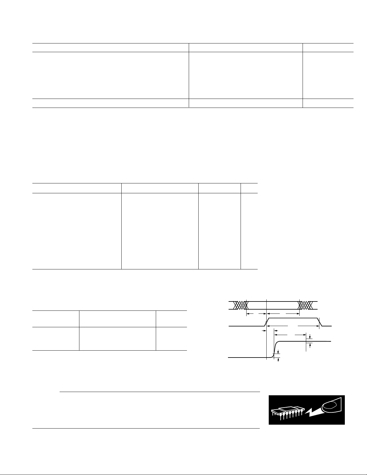
Timing Diagram
CAUTION
ESD (electrostatic discharge) sensitive device. Electrostatic charges as high as 4000 V readily
accumulate on the human body and test equipment and can discharge without detection.
Although the AD768 features proprietary ESD protection circuitry, permanent damage may
occur on devices subjected to high energy electrostatic discharges. Therefore, proper ESD
precautions are recommended to avoid performance degradation or loss of functionality.
REV. B
–3–

AD768
1
WAFER TEST LIMITS
(TA = +258C, VDD = +5.0 V, VEE = –5.0 V, I
Parameter AD768ACHIPS Limit Units
Integral Nonlinearity
Differential Nonlinearity
2
2
±8 LSB max
± 6 LSB max
Offset Error ± 0.2 % FSR max
Gain Error ±1.0 % FSR max
Reference Voltage ±1.0 % of nom. 2.5 V max
Positive Supply Current 40 mA max
Negative Supply Current 73 mA max
Power Dissipation 600 mW max
NOTES
1
Electrical test are performed at wafer probe to the limits shown. Due to variations in assembly methods and normal
yield loss, yield after packaging is not guaranteed for standard product dice.
2
Limits extrapolated from testing of individual bit errors.
3
Die offers latch control pad. Edge triggered latches become level triggered when latch control and clock pads are high.
4
Die substrate is connected to V
EE.
PIN DESCRIPTIONS
Pin No. Symbol Type Name and Function
1 IOUTA AO DAC Current Output. Full-scale current when all data bits are 1s.
2 NR AI Noise Reduction Node. Add capacitor for noise reduction.
3 REFOUT AO Reference Output Voltage. Nominal value is 2.5 V.
4 NC NC No Connect. Reserved for internal use.
5 REFCOM P Reference Ground.
6 IREFIN AI Reference Input Current. Nominal is 5 mA. DAC full-scale is 4× this current.
7 DB0 DI Data Bit 0 (LSB).
8–14 DB1–DB7 DI Data Bits 1–7.
15 DCOM P Digital Ground.
16 CLOCK DI Clock Input. Data latched on positive edge of clock.
17–23 DB8–DB14 DI Data Bits 8–14.
24 DB15 DI Data Bit 15 (MSB).
25 V
26 V
DD
EE
P Positive Supply Voltage. Nominal is +5V.
P Negative Supply Voltage. Nominal is –5V.
27 IOUTB AO Complementary DAC Current Output. Full-scale current when all data bits are 0s.
28 LADCOM P DAC Ladder Common.
Type: AI = Analog Input; DI = Digital Input; AO = Analog Output; P = Power.
= 5 mA, unless otherwise noted)
REFIN
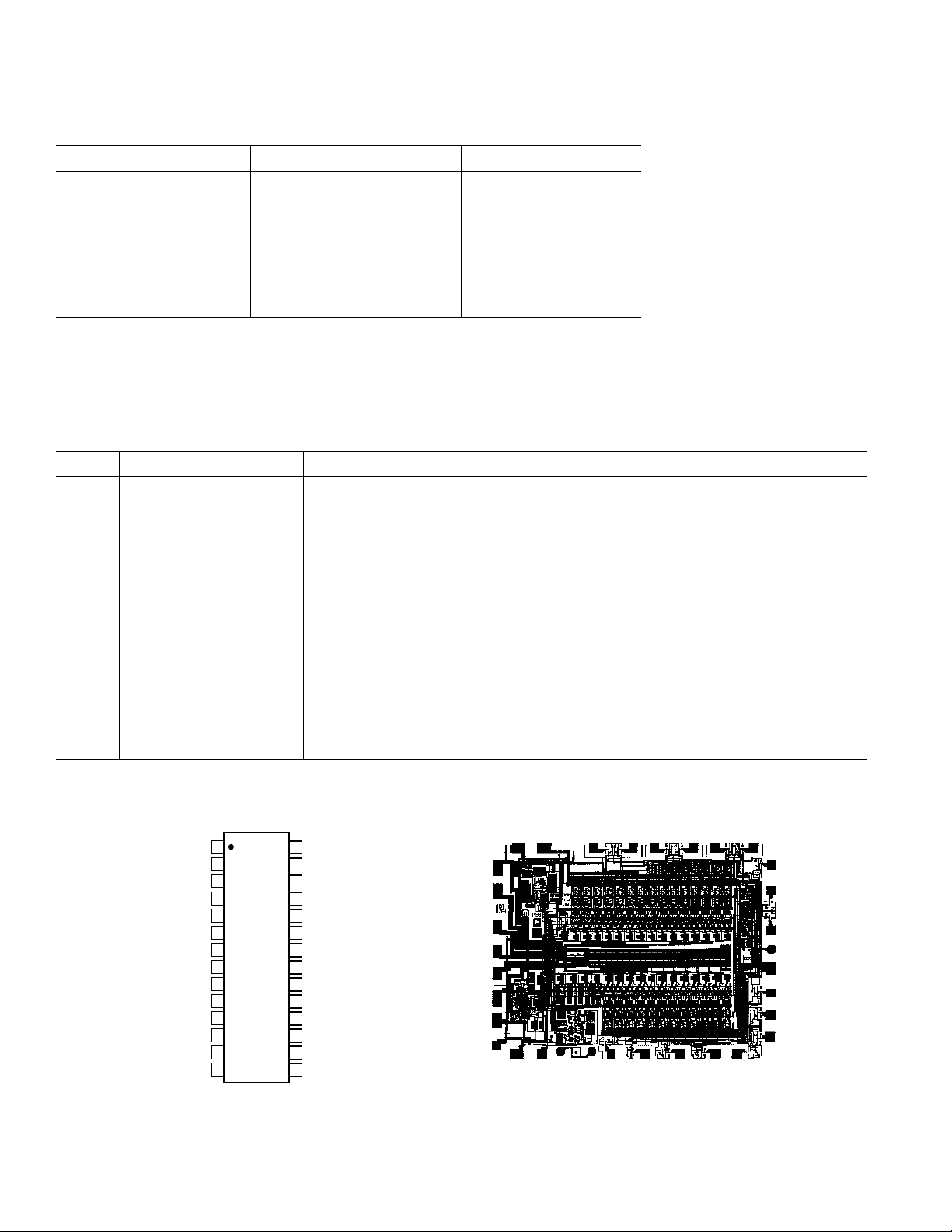
PIN CONFIGURATION
1
IOUTA
NR
REFOUT
NC
REFCOM
IREFIN
(LSB) DB0
DB1
DB2
DB3
DB4
DB5
DB6
DB7
2
3
4
5
6
AD768
TOP VIEW
7
(Not to Scale)
8
9
10
11
12
13
14
NC = NO CONNECT
28
27
26
25
24
23
22
21
20
19
18
17
16
15
LADCOM
IOUTB
(–5V)
V
EE
VDD (+5V)
DB15 (MSB)
DB14
DB13
DB12
DB11
DB10
DB9
DB8
CLOCK
DCOM
DICE CHARACTERISTICS
VDDV
V
EE
V
EE
IOUTB
LADCOM
IOUTA
NR
REFOUT
NC
REFCOM IREFIN DB0 DB1 DB2 DB3 DB4
DB15 DB14 DB13 DB12 DB11 DB10
DD
Die Size:
×
0.1106
(2.81
0.1417 inch, 15,672 sq. mils
×
3.60 mm, 10.116 sq. mm)
–4–
3, 4
DB9
DB8
CLOCK
LATCH CONTROL
DCOM
DB7
DB6
DB5
REV. B

AD768
DEFINITIONS OF SPECIFICATIONS
Linearity Error (Also Called Integral Nonlinearity or INL)
Linearity error is defined as the maximum deviation of the actual analog output from the ideal output, determined by a
straight line drawn from zero to full scale.
Differential Nonlinearity (or DNL)
DNL is the measure of the variation in analog value, normalized
to full scale, associated with a1LSBchangein digital input code.
Monotonicity
A D/A converter is monotonic if the output either increases or
remains constant as the digital input increases.
Offset Error
The deviation of the output current from the ideal of zero is
called offset error. For IOUTA, 0 mA output is expected when
the inputs are all 0s. For IOUTB, 0 mA output is expected
when all inputs are set to 1s.
Gain Error
The difference between the actual and ideal output span. The
actual span is determined by the output when all inputs are set
to 1s minus the output when all inputs are set to 0s. The ideal
output current span is 4× the current applied to the IREFIN pin.
Output Compliance Range
The range of allowable voltage at the output of a current-output
DAC. Operation beyond the maximum compliance limits may
cause either output stage saturation or breakdown, resulting in
nonlinear performance.
C
REFCOMP
R
20
6
DB11
REF
500Ω
REFINREFOUT
19
DB10
+5V
–5V
CLOCK
1µF
1µF
1µF
C
1µF
DB14
AD768
21222324
DB13
DB12
34
NC
V
DD
REFCOM
NR
V
EE
DCOM
CLOCK
+2.5V REF
MSB DECODE
& LATCHES
DB15
25
5
2
NR
26
15
16
Temperature Drift
Temperature drift is specified as the maximum change from the
ambient (+25°C) value to the value at either T
MIN
or T
MAX
. For
offset and gain drift, the drift is reported in ppm of full-scale
range (FSR) per degree C. For reference drift, the drift is reported in ppm per degree C.
Power Supply Rejection
The maximum change in the full-scale output as the supplies
are varied from nominal to minimum and maximum specified
voltages.
Settling Time
The time required for the output to reach and remain within a
specified error band about its final value, measured from the
start of the output transition.
Spurious-Free Dynamic Range
The difference, in dB, between the rms amplitude of the
input signal and the peak spurious signal over the specified
bandwidth.
Total Harmonic Distortion
THD is the ratio of the rms sum of the first six harmonic components to the rms value of the measured input signal. It is expressed as a percentage or in decibels (dB).
Glitch Impulse
Asymmetrical switching times in a DAC give rise to undesired
output transients which are quantified by a glitch impulse. It is
specified as the net area of the glitch in pV-sec.
IOUTA
5mA
SEGMENTED
CURRENT
SOURCES
LATCHES – LOWER 12 BITS
DB7
DB9
DB8
13141718
DB5
DB6
CURRENT SOURCES
AND R-2R LADDER
DB4
R
1kΩ
LAD
DB3
R
1kΩ
LADCOM
89101112
DB2
LAD
DB1
IOUTB
7
DB0
1
27
50Ω
28
R
50Ω
IOUTA
IOUTB
LOAD
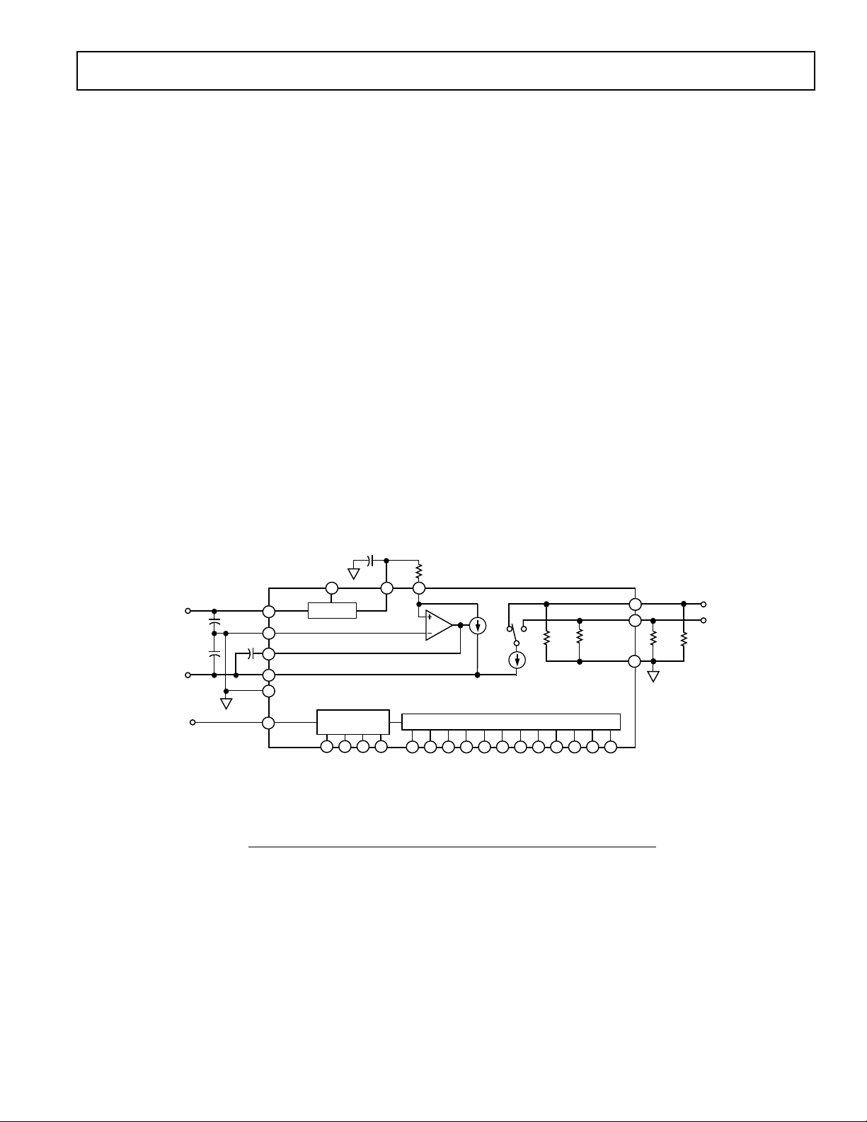
Figure 1. Functional Block Diagram and Basic Hookup
FUNCTIONAL DESCRIPTION
The AD768 is a current-output DAC with a nominal full-scale
current of 20 mA and a 1 kΩ output impedance. Differential
outputs are provided to support single-ended or differential
applications. The DAC architecture combines segmented current sources for the top four bits (MSBs) and a 1kΩ R-2R ladder for the lower 12 bits (LSBs). The DAC current sources are
implemented with laser-trimmable thin film resistors for excellent dc linearity. A proprietary switching technique is utilized to
reduce glitch energy and maximize dynamic accuracy.
REV. B
–5–
The digital interface offers CMOS compatible edge-triggered
input latches that interface readily to CMOS logic and supports
clock rates up to 40 MSPS. A temperature compensated 2.5V
bandgap reference is integrated on-chip to drive the AD768 reference input current with the use of a single external resistor.
The functional block diagram in Figure 1 is a simple representation of the internal circuitry to aid the understanding of the
AD768’s operation. The DAC transfer function is described,
and followed by a detailed description of each key portion of the
circuit. Typical circuit configurations are shown in the section
APPLYING THE AD768.

AD768
I
REFIN
– mA
POWER – mW
550
500
300
1.0 7.02.0 3.0 4.0 5.0 6.0
450
400
350
DAC TRANSFER FUNCTION
The AD768 may be used in either current-output mode with the
output connected to a virtual ground, or voltage-output mode
with the output connected to a resistive load.
In current output mode,
I
= (DAC CODE/65536) × (I
OUT
In voltage output mode,
= I
V
OUT
OUT
× R
LOADiRLAD
where:
DAC CODE is the decimal representation of the DAC inputs;
an integer between 0 and 65535.
I
is the current applied at the IREFIN pin, determined by
REFIN
V
REF/RREF
Substituting for I
V
OUT
= –V
.
and I
OUT
× (DAC CODE/65536) × 4 × [(R
REF
REFIN
,
These equations clarify an important aspect of the AD768
transfer function; the full-scale current output of the DAC is
proportional to a current input. The voltage output is then a
function of the ratio of (R
LOADiRLAD
)/R
REF
lation of resistor drift by selection of resistors with matched
characteristics.
REFERENCE INPUT
The IREFIN pin is a current input node with low impedance to
REFCOM. This input current sets the magnitude of the DAC
current sources such that the full-scale output current is exactly
four times the current applied at IREFIN. For the nominal input current of 5 mA, the nominal full-scale output current is
20 mA.
The 5 mA reference input current can be generated from the
on-chip 2.5 V reference with an external resistor of 500 Ω from
REFOUT to IREFIN. If desired, a variety of external reference
voltages may be used based on the selection of an appropriate
resistor. However, to maintain stability of the reference amplifier, the external impedance at IREFIN must be kept below
1kΩ.
IREFIN
5
6
V
EE
REFCOM
× 4)
REFIN
LOADiRLAD
)/R
REF
, allowing for cancel-
IFB
5mA
V
EE
]
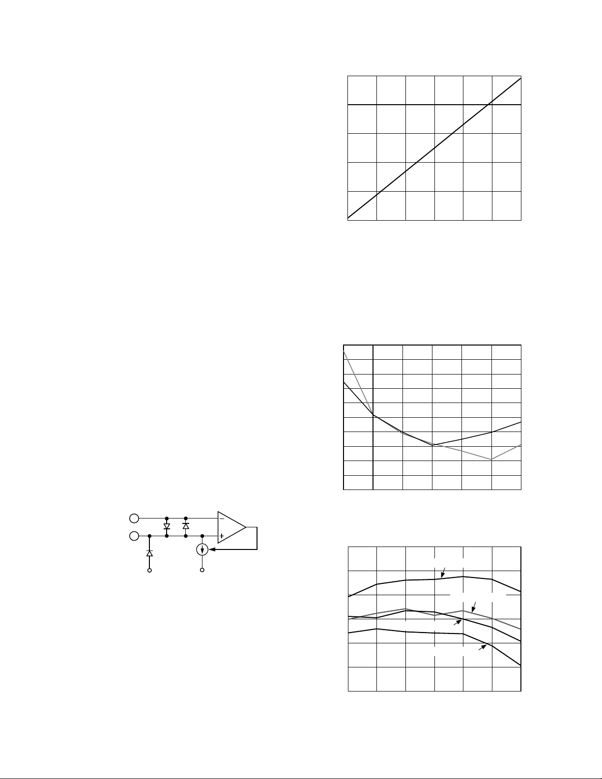
Figure 3. Power Dissipation vs. I
REFIN
Current
Note the AD768 is optimized for operation at an input current
of 5 mA. Both linearity and dynamic performance at other input
currents may be somewhat degraded. Figure 4 shows typical dc
linearity over a range of input currents. Figure 5 shows typical
SFDR (to Nyquist) performance over a range of input currents
and CLOCK input rates for a 1 MHz output frequency.
10
9
8
7
6
5
4
ERROR – LSB
3
2
1
0
1.0 7.02.0 3.0 4.0 5.0 6.0
I
REFIN
– mA
Figure 4. INL/DNL vs. I
–85
–80
CLOCK = 10 MSPS
REFIN
INL
DNL
Current
The I
current can be varied from 1 mA to 7 mA which
REFIN
subsequently will result in a proportional change in the DAC
Figure 2. Equivalent Reference Input Circuit
full-scale. Since the operating currents within the DAC vary
with I
, so does the power dissipation. Figure 3 illustrates
REFIN
that relationship.
–6–
–75
–70
SFDR – dB
–65
–60
–55
1.0 7.02.0 3.0 4.0 5.0 6.0
CLOCK = 30 MSPS
CLOCK = 40 MSPS
I
– mA
REFIN
Figure 5. SFDR (to Nyquist) vs. I
CLOCK = 20 MSPS
@ F
REFIN
OUT
= 1 MHz
REV. B
 Loading...