16-Bit, 8-Channel,
www.BDTIC.com/ADI
250 kSPS PulSAR® ADC
Preliminary Technical Data
FEATURES
16-bit resolution with no missing codes
8-channel multiplexer with:
Unipolar single ended or
Differential (GND sense)/pseudo-bipolar inputs
Throughput: 250 kSPS
INL/DNL: ±0.6 LSB typical
Dynamic range: 93.5 dB
SINAD: 92.5 dB @ 20 kHz
THD: −100 dB @ 20 kHz
Analog input range:
0 V to V
with V
REF
up to VDD
REF
Reference:
Internal selectable 2.5 V/4.096 V or
External buffered (up to 4.096 V)
External (up to VDD)
Internal temperature sensor
Channel sequencer, selectable 1-pole filter, BUSY indicator
No pipeline delay, SAR architecture
Single-supply 2.7V – 5.5 V operation with
1.8 V to 5 V logic interface
Serial interface SPI®/QSPI™/MICROWIRE™/DSP compatible
Power dissipation:
6 mW @ 5 V/100 kSPS
Standby current: 1 nA
20-lead 4 mm × 4 mm LFCSP package
APPLICATIONS
Battery-powered equipment
Medical instruments
Mobile communications
Personal digital assitants
Data acquisition
Seismic data acquisition systems
Instrumentation
Process Control
IN0
IN1
IN2
IN3
IN4
IN5
IN6
IN7
COM
Table 1. Multichannel14-/16-Bit PulSAR ADC
Type Channels
14-Bit 8 AD7949 ADA4841-x
16-Bit 4 AD7682 ADA4841-x
16-Bit 8 AD7689 AD7699 ADA4841-x
GENERAL DESCRIPTION
The AD7689 is an 8-channel 16-bit, charge redistribution
successive approximation register (SAR), analog-to-digital
converter (ADC) that operates from a single power supply, VDD.
The AD7689 contains all of the components for use in a multichannel, low power, data acquisition system including: a true 16-bit
SAR ADC with no missing codes; an 8-channel, low crosstalk
multiplexer useful for configuring the inputs as single ended (with
or without ground sense), differential or bipolar; an internal low
drift reference (selectable 2.5V or 4.096V) and buffer; a
temperature sensor; a selectable 1-pole filter; and a sequencer
useful when channels are continuously scanned in order.
The AD7689 uses a simple SPI interface for writing to the
configuration register and receiving conversion results. The SPI
interface uses a separate supply, VIO, which is set to the host logic
level.
Power dissipation scales with throughput.
The AD7689 is housed in a tiny 20-lead LFCSP with operation
specified from −40°C to +85°C.
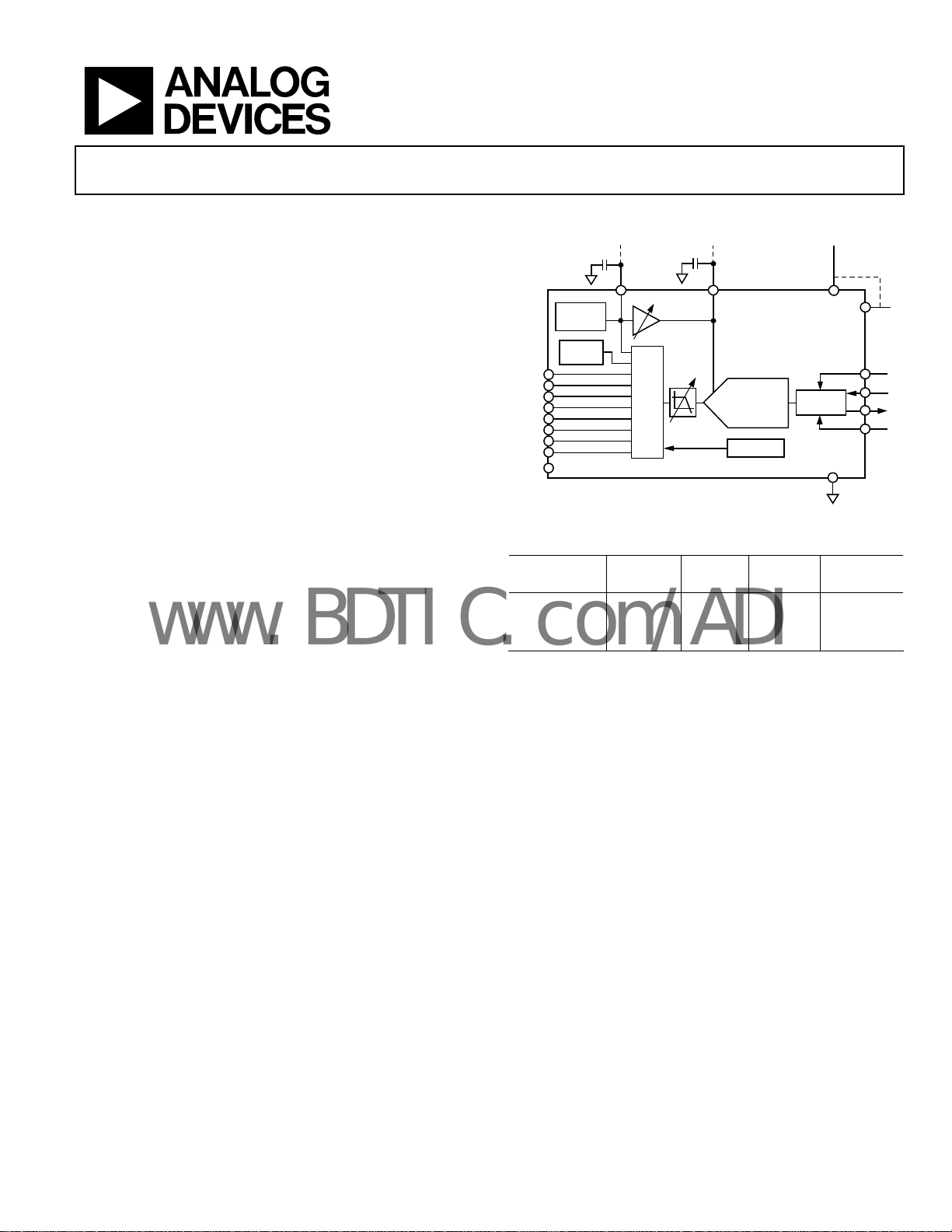
FUNCTIONAL BLOCK DIAGRAM
0.5V to 4.096V
Band Gap
REF
Temp
Sensor
0.1μF
REFIN
MUX
0.5V to VDD
22μF
1-Pole
LPF
Figure 1.
250
kSPS
REF
16-Bit SAR
ADC
Sequencer
500
kSPS
AD7689
2.7V to 5V
VDD
AD7689
SPI Serial
Interface
GND
ADC
Driver
VIO
1.8V to
VDD
CNV
SCK
SDO
DIN
Rev. PrD
Information furnished by Analog Devices is believed to be accurate and reliable. However, no
responsibility is assumed by Anal og Devices for its use, nor for any infringements of patents or ot her
rights of third parties that may result from its use. Specifications subject to change without notice. No
license is granted by implication or otherwise under any patent or patent rights of Analog Devices.
Trademarks and registered trademarks are the property of their respective owners.
One Technology Way, P.O. Box 9106, Norwood, MA 02062-9106, U.S.A.
Tel: 781.329.4700 www.analog.com
Fax: 781.461.3113 ©2008 Analog Devices, Inc. All rights reserved.

AD7689 Preliminary Technical Data
www.BDTIC.com/ADI
TABLE OF CONTENTS
Features.............................................................................................. 1
Applications....................................................................................... 1
Functional Block Diagram ..............................................................1
General Description......................................................................... 1
Revision History ...............................................................................2
Specifications..................................................................................... 3
Timing Specifications....................................................................... 5
Absolute Maximum Ratings............................................................ 7
ESD Caution.................................................................................. 7
Pin Configurations and Function Descriptions........................... 8
Typical Performance Characteristics............................................. 9
Terminology.................................................................................... 10
Theory of Operation ......................................................................11
Overview...................................................................................... 11
Converter Operation.................................................................. 11
Transfer Functions......................................................................12
Typical Connection Diagram ................................................... 12
Analog Inputs..............................................................................13
Driver Amplifier Choice............................................................ 14
Voltage Reference Output/Input .............................................. 14
Power Supply............................................................................... 15
Supplying the ADC from the Reference.................................. 15
Digital Interface.............................................................................. 16
Configuration Register, CFG.................................................... 16
R/W During Convert, NO Busy Indicator.............................. 18
R/W During Convert, With Busy Indicator............................ 19
Application Hints ........................................................................... 20
Layout .......................................................................................... 20
Evaluating AD7689 Performance............................................. 20
Outline Dimensions....................................................................... 21
Ordering Guide .......................................................................... 21
REVISION HISTORY
Rev. PrD | Page 2 of 21

Preliminary Technical Data AD7689
www.BDTIC.com/ADI
SPECIFICATIONS
VDD = 2.5 V to 5.5 V, VIO = 2.3 V to VDD, V
Table 2.
Parameter Conditions/Comments Min Typ Max Unit
RESOLUTION 16 Bits
ANALOG INPUT
Voltage Range Unipolar mode 0 +V
Bipolar mode −V
Absolute Input Voltage
Analog Input CMRR fIN = 250 kHz TBD dB
Leakage Current at 25°C Acquisition phase 1 nA
Input Impedance1
THROUGHPUT
Conversion Rate VDD = 4.5 V to 5.5 V 0 250 kSPS
VDD = 2.5 V to 4.5 V 1 200
Transient Response Full-scale step 1.8
ACCURACY
No Missing Codes 16 Bits
Integral Linearity Error -2 ±0.6 +2 LSB2
Differential Linearity Error −1 ±0.25 +1.5 LSB
Transition Noise REF = VDD = 5 V 0.5 LSB
Gain Error3 −30 ±0.5 +30 LSB
Gain Error Match TBD LSB
Gain Error Temperature Drift ±0.3 ppm/°C
Offset Error3 −5 ±0.5 +5 LSB
Offset Error Match TBD LSB
Offset Error Temperature Drift ±0.3 ppm/°C
Power Supply Sensitivity
AC ACCURACY4
Dynamic Range 93.5 dB5
Signal-to-Noise6 f
f
Signal-to-(Noise + Distortion)6 f
f
Total Harmonic Distortion fIN = 20 kHz −100 dB
Spurious-Free Dynamic Range fIN = 20 kHz 110 dB
Channel-to-Channel Crosstalk
Intermodulation Distortion7 115 dB
SAMPLING DYNAMICS
−3 dB Input Bandwidth Selectable 0.425 1.7 MHz
Aperture Delay VDD = 5V 2.5 ns
1
See the Analog Inputs section.
2
LSB means least significant bit. With the 5 V input range, one LSB is 76.3 µV.
3
See the Terminology section. These specifications include full temperature range variation but not the error contribution from the external reference.
4
With V
= 5 V, unless otherwise noted.
REF
5
All specifications expressed in decibels are referred to a full-scale input FSR and tested with an input signal at 0.5 dB below full scale, unless otherwise specified.
6
VDD = 5V.
7
f
= 21.4 kHz and f
IN1
= 18.9 kHz, with each tone at −7 dB below full scale.
IN2
= VDD, all specifications T
REF
Positive input, unipolar and
MIN
to T
, unless other wise noted.
MAX
/2 +V
REF
−0.1 V
V
REF
/2
REF
+ 0.1 V
REF
bipolar mode
Negative or COM input, unipolar
−0.1 +0.1
mode
Negative or COM input, bipolar
/2 – 0.1 V
REF
/2 V
REF
/2 + 0.1
REF
V
mode
VDD = 5 V ± 5%
= 20 kHz, VREF = 5V 92.5 dB
IN
= 20 kHz, VREF = 2.5V 88.5
IN
= 20 kHz, VREF = 5V 92.5 dB
IN
= 20 kHz, VREF = 2.5V 88.5 dB
IN
= 100 kHz on adjacent
f
IN
±1 ppm
-117 dB
channel(s)
Rev. PrD | Page 3 of 21
μs

AD7689 Preliminary Technical Data
www.BDTIC.com/ADI
VDD = 2.5 V to 5.5 V, VIO = 2.3 V to VDD, V
Table 3.
Parameter Conditions/Comments Min Typ Max Unit
INTERNAL REFERENCE
REF Output Voltage 2.5 V, @ 25°C 2.490 2.500 2.510
4.096 V, @ 25°C 4.086 4.096 4.106
REFIN Output Voltage1 2.5 V, @ 25°C 1.2
4.096 V, @ 25°C 2.3
REF Output Current –40°C to +85°C ±300 µA
Temperature Drift –40°C to +85°C ±TBD
Line Regulation VDD = 5 V ± 5% ±TBD
Long-Term Drift 1000 hours 50
Turn-On Settling Time C
EXTERNAL REFERENCE
Voltage Range REF Input 0.5 VDD + 0.3 V
REFIN Input (Buffered) 0.5 VDD – 0.2 V
Current Drain 250 kSPS, REF = 5V 50 µA
TEMPERATURE SENSOR
Output Voltage2 @ 25°C 283 mV
Temperature Sensitivity 1 mV/°C
DIGITAL INPUTS
Logic Levels
VIL −0.3 +0.3 × VIO V
VIH 0.7 × VIO VIO + 0.3 V
IIL −1 +1 µA
IIH −1 +1 µA
DIGITAL OUTPUTS
Data Format3
Pipeline Delay4
VOL I
VOH I
POWER SUPPLIES
VDD Specified performance 2.3 5.5 V
VIO Specified performance 2.3 VDD + 0.3 V
VIO Range 1.8 VDD + 0.3 V
Standby Current
5, 6
VDD and VIO = 5 V, 25°C 1 50 nA
Power Dissipation VDD = 5V , 100 kSPS throughput 6 mW
VDD = 5V , 250 kSPS throughput 15 mW
Energy per Conversion 50 nJ
TEMPERATURE RANGE7
Specified Performance T
1
This is the output from the internal band-gap.
2
The output voltage is internal and present on a dedicated multiplexer input.
3
Unipolar mode: serial 16-bit straight binary
Bipolar mode: serial 16-bit 2’s complement.
4
Conversion results available immediately after completed conversion.
5
With all digital inputs forced to VIO or GND as required.
6
During acquisition phase.
7
Contact an Analog Devices sales representative for the extended temperature range.
= VDD, all specifications T
REF
= 22 µF TBD
REF
= +500 µA 0.4 V
SINK
= −500 µA VIO − 0.3 V
SOURCE
VDD = 5V , 250 kSPS throughput
to T
MIN
, unless other wise noted.
MAX
18.5 mW
internal reference and buffer
enabled
to T
MIN
−40 +85 °C
MAX
V
V
V
V
ppm/°C
ppm/V
ppm
ms
Rev. PrD | Page 4 of 21

Preliminary Technical Data AD7689
www.BDTIC.com/ADI
TIMING SPECIFICATIONS
VDD = 4.5 V to 5.5 V, VIO = 2.3 V to VDD, all specifications T
Table 4.
1
Parameter Symbol Min Typ Max Unit
Conversion Time: CNV Rising Edge to Data Available t
Acquisition Time t
Time Between Conversions t
CNV Pulse Width t
Data Write/Read During Conversion t
SCK Period t
SCK Low Time t
SCK High Time t
SCK Falling Edge to Data Remains Valid t
SCK Falling Edge to Data Valid Delay t
VIO Above 4.5 V 14 ns
VIO Above 3 V 15 ns
VIO Above 2.7 V 16 ns
VIO Above 2.3 V 17 ns
CNV Low to SDO D15 MSB Valid tEN
VIO Above 4.5 V 15 ns
VIO Above 2.7 V 18 ns
VIO Above 2.3 V 22 ns
CNV High or Last SCK Falling Edge to SDO High Impedance t
CNV Low to SCK Rising Edge t
DIN Valid Setup Time from SCK Falling Edge t
DIN Valid Hold Time from SCK Falling Edge t
1
See Figure 2 and Figure 3 for load conditions.
MIN
to T
, unless otherwise noted.
MAX
2.2 µs
CONV
1.8 µs
ACQ
4 µs
CYC
10 ns
CNVH
1.5 µs
DATA
15 ns
SCK
7 ns
SCKL
7 ns
SCKH
4 ns
HSDO
DSDO
25 ns
DIS
TBD ns
CLSCK
4 ns
SDIN
4 ns
HDIN
Rev. PrD | Page 5 of 21

AD7689 Preliminary Technical Data
T
2
www.BDTIC.com/ADI
VDD = 2.5 V to 4.5 V, VIO = 2.3 V to VDD, all specifications T
1
Table 5.
Parameter Symbol Min Typ Max Unit
Conversion Time: CNV Rising Edge to Data Available t
Acquisition Time t
Time Between Conversions t
CNV Pulse Width t
Data Write/Read During Conversion t
SCK Period t
SCK Low Time t
SCK High Time t
SCK Falling Edge to Data Remains Valid t
SCK Falling Edge to Data Valid Delay t
VIO Above 3 V 24 ns
VIO Above 2.7 V 30 ns
VIO Above 2.3 V 35 ns
CNV Low to SDO D15 MSB Valid tEN
VIO Above 2.7 V 18 ns
VIO Above 2.3 V 22 ns
CNV High or Last SCK Falling Edge to SDO High Impedance t
CNV Low to SCK Rising Edge t
SDI Valid Setup Time from SCK Falling Edge t
SDI Valid Hold Time from SCK Falling Edge t
1
See Figure 2 and Figure 3 for load conditions.
MIN
to T
, unless otherwise noted.
MAX
3.2 µs
CONV
1.8 µs
ACQ
5 µs
CYC
10 ns
CNVH
0.7 µs
DATA
25 ns
SCK
12 ns
SCKL
12 ns
SCKH
5 ns
HSDO
DSDO
25 ns
DIS
TBD ns
CLSCK
5 ns
SDIN
4 ns
HDIN
O SDO
50pF
C
L
500µA I
500µA I
OL
OH
1.4V
00
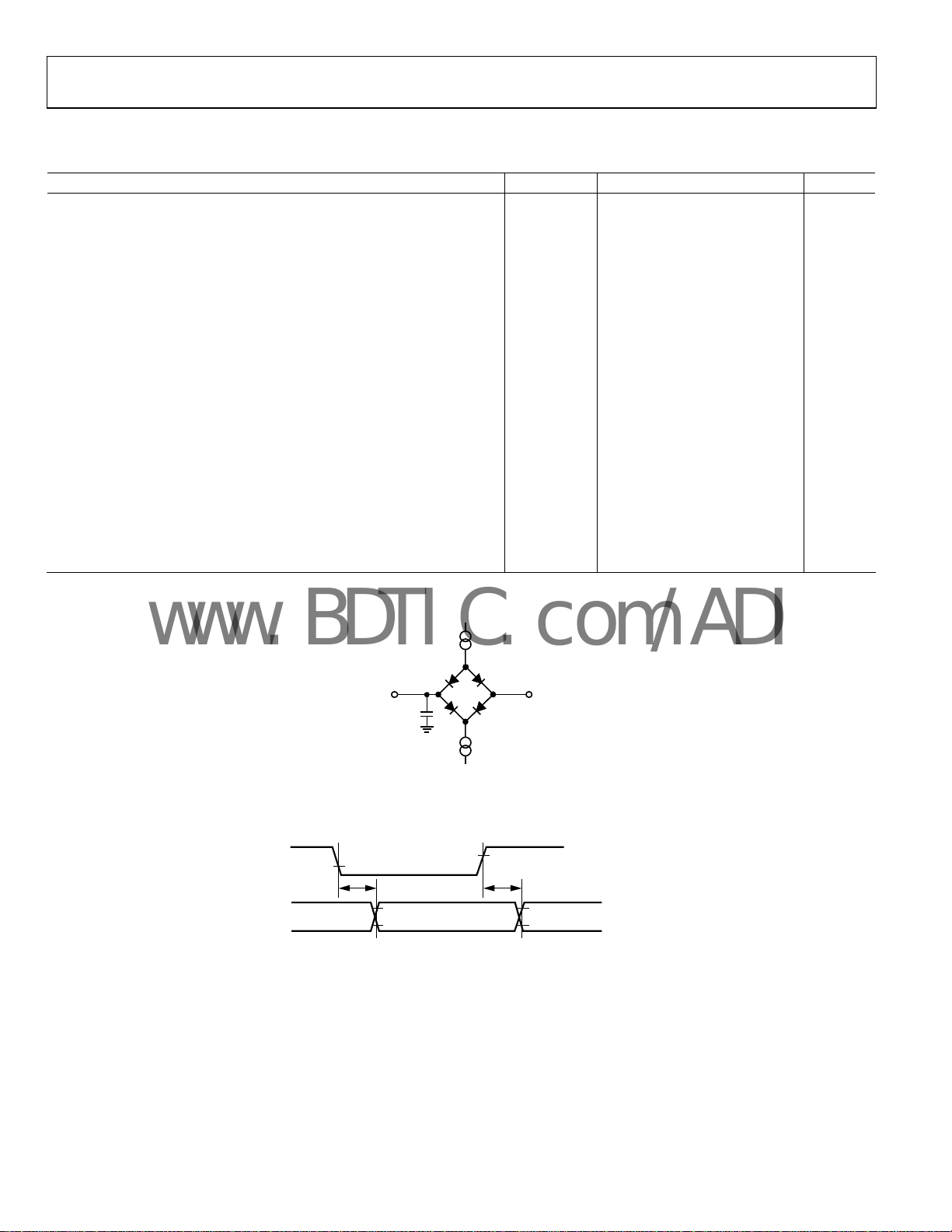
Figure 2. Load Circuit for Digital Interface Timing
30% VIO
t
DELAY
2V OR VIO – 0.5V
0.8V OR 0. 5V
1. 2V IF VIO ABOVE 2.5V, VIO – 0.5V IF V IO BELOW 2.5V.
2. 0.8V IF VIO ABOVE 2.5 V , 0.5V I F VIO BELOW 2.5V.
Figure 3. Voltage Levels for Timing
70% VIO
t
DELAY
1
2
2V OR VIO – 0.5V
0.8V OR 0.5 V
1
2
003
Rev. PrD | Page 6 of 21

Preliminary Technical Data AD7689
www.BDTIC.com/ADI
ABSOLUTE MAXIMUM RATINGS
Table 6.
Parameter Rating
Analog Inputs
INn,1 COM1
REF, REFIN GND − 0.3 V to VDD + 0.3 V
Supply Voltages
VDD, VIO to GND −0.3 V to +7 V
VDD to VIO ±7 V
DIN, CNV, SCK to GND −0.3 V to VIO + 0.3 V
SDO to GND −0.3 V to VIO + 0.3 V
Storage Temperature Range −65°C to +150°C
Junction Temperature 150°C
θJA Thermal Impedance (MSOP-10) 200°C/W
θJC Thermal Impedance (MSOP-10) 44°C/W
1
See Analog Inputs section.
GND − 0.3 V to VDD + 0.3 V
or ±130 mA
Stresses above those listed under Absolute Maximum Ratings
may cause permanent damage to the device. This is a stress
rating only; functional operation of the device at these or any
other conditions above those indicated in the operational
section of this specification is not implied. Exposure to absolute
maximum rating conditions for extended periods may affect
device reliability.
ESD CAUTION
Rev. PrD | Page 7 of 21
 Loading...