

Analog Devices AD7683 Datasheet
16-Bit, 100 kSPS PulSAR
FEATURES
16-bit resolution with no missing codes
Throughput: 100 kSPS
INL: ±1 LSB typ, ±3 LSB max
Pseudodifferential analog input range
0 V to V
with V
REF
Single-supply operation: 2.7 V to 5.5 V
Serial interface SPI®/QSPI™/MICROWIRE™/DSP-compatible
Power dissipation : 4 mW @ 5 V, 1.5 mW @ 2.7 V,
150 µW @ 2.7 V/10 kSPS
Standby current: 1 nA
8-lead package: MSOP package and
3 mm × 3 mm QFN
Improved 2
APPLICATIONS
Battery-powered equipment
Data acquisition
Instrumentation
Medical instruments
Process control
up to VDD
REF
1
nd
source to ADS8320 and ADS8325
(LFCSP) (SOT-23 size)
ADC in MSOP/QFN
AD7683
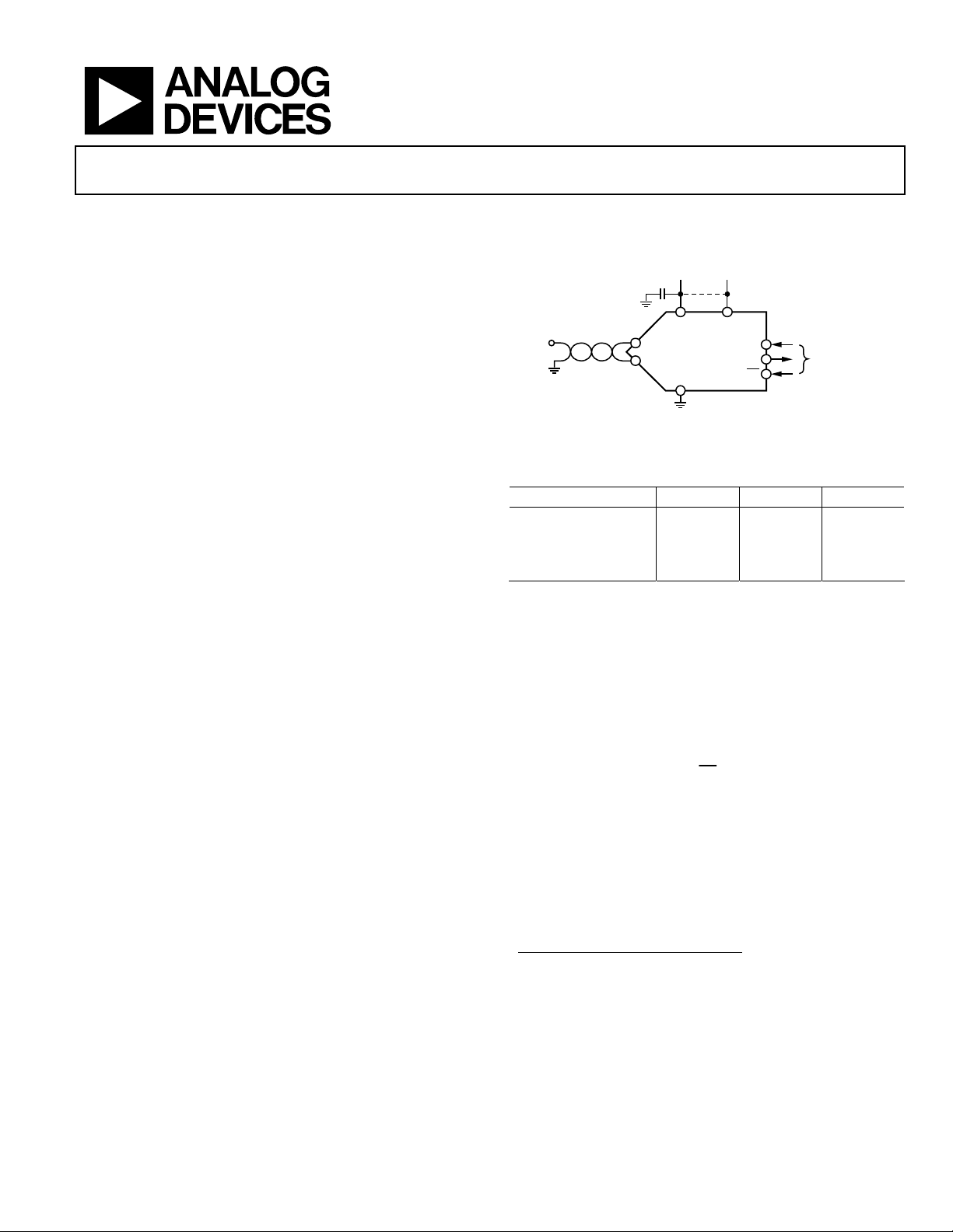
APPLICATION DIAGRAM
0.5V TO VDD 2.7V TO 5.5V
REF
0 TO V
REF
+IN
–IN
Table 1. MSOP, QFN (LFCSP)/SOT-23, 16-Bit PulSAR ADC
Type 100 kSPS 250 kSPS 500 kSPS
True Differential AD7684 AD7687 AD7688
Pseudo
AD7683
Differential/Unipolar
Unipolar AD7680
GENERAL DESCRIPTION
The AD7683 is a 16-bit, charge redistribution, successive
approximation, PulSAR™ analog-to-digital converter (ADC)
that operates from a single power supply, VDD, between 2.7 V
to 5.5 V. It contains a low power, high speed, 16-bit sampling
ADC with no missing codes (B grade), an internal conversion
clock, and a serial, SPI-compatible interface port. The part also
contains a low noise, wide bandwidth, short aperture delay,
track-and-hold circuit. On the
analog input, +IN, between 0 V to REF with respect to a ground
sense, –IN. The reference voltage, REF, is applied externally and
can be set up to the supply voltage. Its power scales linearly with
throughput.
VDD
DCLOCK
AD7683
GND
Figure 1.
D
OUT
CS
AD7685
AD7694
falling edge, it samples an
CS
3-WIRE SPI
INTERFACE
AD7686
04301-001
Rev. 0
Information furnished by Analog Devices is believed to be accurate and reliable.
However, no responsibility is assumed by Analog Devices for its use, nor for any
infringements of patents or other rights of third parties that may result from its use.
Specifications subject to change without notice. No license is granted by implication
or otherwise under any patent or patent rights of Anal og Devices. Trademarks and
registered trademarks are the property of their respective owners.
The AD7683 is housed in an 8-lead MSOP or an 8-lead QFN
(LFCSP) package, with an operating temperature specified from
−40°C to +85°C.
1
QFN package in development. Contact factory for samples and availability.
One Technology Way, P.O. Box 9106, Norwood, MA 02062-9106, U.S.A.
Tel: 781.329.4700
Fax: 781.326.8703 © 2004 Analog Devices, Inc. All rights reserved.
www.analog.com

AD7683
TABLE OF CONTENTS
Specifications..................................................................................... 3
Typical C o n n e ction Di ag r a m ................................................... 13
Timing Specifications....................................................................... 5
Absolute Maximum Ratings............................................................ 6
ESD Caution.................................................................................. 6
Pin Configuration and Functional Descriptions.......................... 7
Te r m in o l o g y ...................................................................................... 8
Typical Performance Characteristics ............................................. 9
Application Information................................................................ 12
Circuit Information.................................................................... 12
Converter Operation.................................................................. 12
Transfe r F u ncti o n s ...................................................................... 12
REVISION HISTORY
9/04—Initial Version: Revision 0
Analog Input............................................................................... 13
Driver Amplifier Choice............................................................ 13
Voltage Reference Input ............................................................ 14
Power Supply............................................................................... 14
Digital Interface.......................................................................... 14
Layout .......................................................................................... 14
Evaluating the AD7683’s Performance.................................... 14
Outline Dimensions....................................................................... 15
Ordering Guide .......................................................................... 15
Rev. 0 | Page 2 of 16

AD7683
SPECIFICATIONS
VDD = 2.7 V to 5.5 V; V
Table 2.
AD7683 All Grades
Parameter Conditions Min Typ Max Unit
RESOLUTION 16 Bits
ANALOG INPUT
Voltage Range +IN − (–IN) 0 V
Absolute Input Voltage +IN −0.1 VDD + 0.1 V
−IN −0.1 0.1 V
Analog Input CMRR fIN = 100 kHz 65 dB
Leakage Current at 25°C Acquisition phase 1 nA
Input Impedance See the Analog Input section.
THROUGHPUT SPEED
Complete Cycle 10 µS
Throughput Rate 0 100 kSPS
DCLOCK Frequency 0 2.9 MHz
REFERENCE
Voltage Range 0.5 VDD + 0.3 V
Load Current 100 kSPS, V
DIGITAL INPUTS
Logic Levels
V
IL
V
IH
I
IL
I
IH
Input Capacitance 5 pF
DIGITAL OUTPUTS
Data Format Serial, 16 bits straight binary.
V
OH
V
OL
POWER SUPPLIES
VDD Specified performance 2.7 5.5 V
VDD Range
1
Operating Current 100 kSPS throughput
VDD VDD = 5 V 800 µA
VDD = 2.7 V 560 µA
Standby Current
Power Dissipation VDD = 5 V 4 6 mW
VDD = 2.7 V 1.5 mW
VDD = 2.7 V, 10 kSPS throughput2 150 µW
TEMPERATURE RANGE
Specified Performance T
= VDD; TA = –40°C to +85°C, unless otherwise noted.
REF
− V
= V
+IN
−IN
/2 = 2.5 V 50 µA
REF
−0.3 0.3 × VDD V
0.7 × VDD VDD + 0.3 V
−1 +1 µA
−1 +1 µA
I
= −500 µA VDD − 0.3 V
SOURCE
I
= +500 µA 0.4 V
SINK
2.0 5.5 V
2, 3
VDD = 5 V, 25°C
to T
MIN
MAX
REF
V
1 50 nA
−40 +85
°C
1
See the section for more information. Typical Performance Characteristics
2
With all digital inputs forced to VDD or GND, as required.
3
During acquisition phase.
Rev. 0 | Page 3 of 16

AD7683
VDD = 5 V; V
Table 3.
A Grade B Grade
Parameter Conditions Min Typ Max Min Typ Max Unit
ACCURACY
No Missing Codes 15 16 Bits
Integral Linearity Error −6 ±3 +6 −3 ±1 +3 LSB
Transition Noise 0.5 0.5 LSB
Gain Error1, T
Gain Error Temperature Drift ±0.3 ±0.3 ppm/°C
Offset Error1, T
Offset Temperature Drift ±0.3 ±0.3 ppm/°C
Power Supply Sensitivity
AC ACCURACY
Signal-to-Noise fIN = 1 kHz 90 88 91 dB
Spurious-Free Dynamic Range fIN = 1 kHz −100 −108 dB
Total Harmonic Distortion fIN = 1 kHz −100 −106 dB
Signal-to-(Noise + Distortion) fIN = 1 kHz 90 88 91 dB
Effective Number of Bits fIN = 1 kHz 14.7 14.8 Bits
= VDD; TA = –40°C to +85°C, unless otherwise noted.
REF
MIN
MIN
to T
to T
MAX
MAX
±2 ±24 ±2 ±15 LSB
±0.7 ±1.6 ±0.4 ±1.6 mV
VDD = 5 V ±5%
±0.05 ±0.05 LSB
2
1
See the section. These specifications include full temperature range variation, but do not include the error contribution from the external reference. Terminology
2
All specifications in dB are referred to a full-scale input, FS. Tested with an input signal at 0.5 dB below full scale, unless otherwise specified.
VDD = 2.7 V; V
= 2.5V; TA = –40°C to +85°C, unless otherwise noted.
REF
Table 4.
A Grade B Grade
Parameter Conditions Min Typ Max Min Typ Max Unit
ACCURACY
No Missing Codes 15 16 Bits
Integral Linearity Error −6 ±3 +6 −3 ±1 +3 LSB
Transition Noise 0.85 0.85 LSB
Gain Error1, T
MIN
to T
MAX
±2 ±30 ±2 ±15 LSB
Gain Error Temperature Drift ±0.3 ±0.3 ppm/°C
Offset Error1, T
MIN
to T
MAX
±0.7 ±3.5 ±0.7 ±3.5 mV
Offset Temperature Drift ±0.3 ±0.3 ppm/°C
Power Supply Sensitivity
VDD = 2.7 V ±5%
±0.05 ±0.05 LSB
AC ACCURACY
Signal-to-Noise fIN = 1 kHz 85 86 dB
2
Spurious-Free Dynamic Range fIN = 1 kHz −96 −100 dB
Total Harmonic Distortion fIN = 1 kHz −94 −98 dB
Signal-to-(Noise + Distortion) fIN = 1 kHz 85 86 dB
Effective Number of Bits fIN = 1 kHz 13.8 14 Bits
1
See the section. These specifications do include full temperature range variation, but do not include the error contribution from the external reference. Terminology
2
All specifications in dB are referred to a full-scale input FS. Tested with an input signal at 0.5 dB below full scale, unless otherwise specified.
Rev. 0 | Page 4 of 16
AD7683
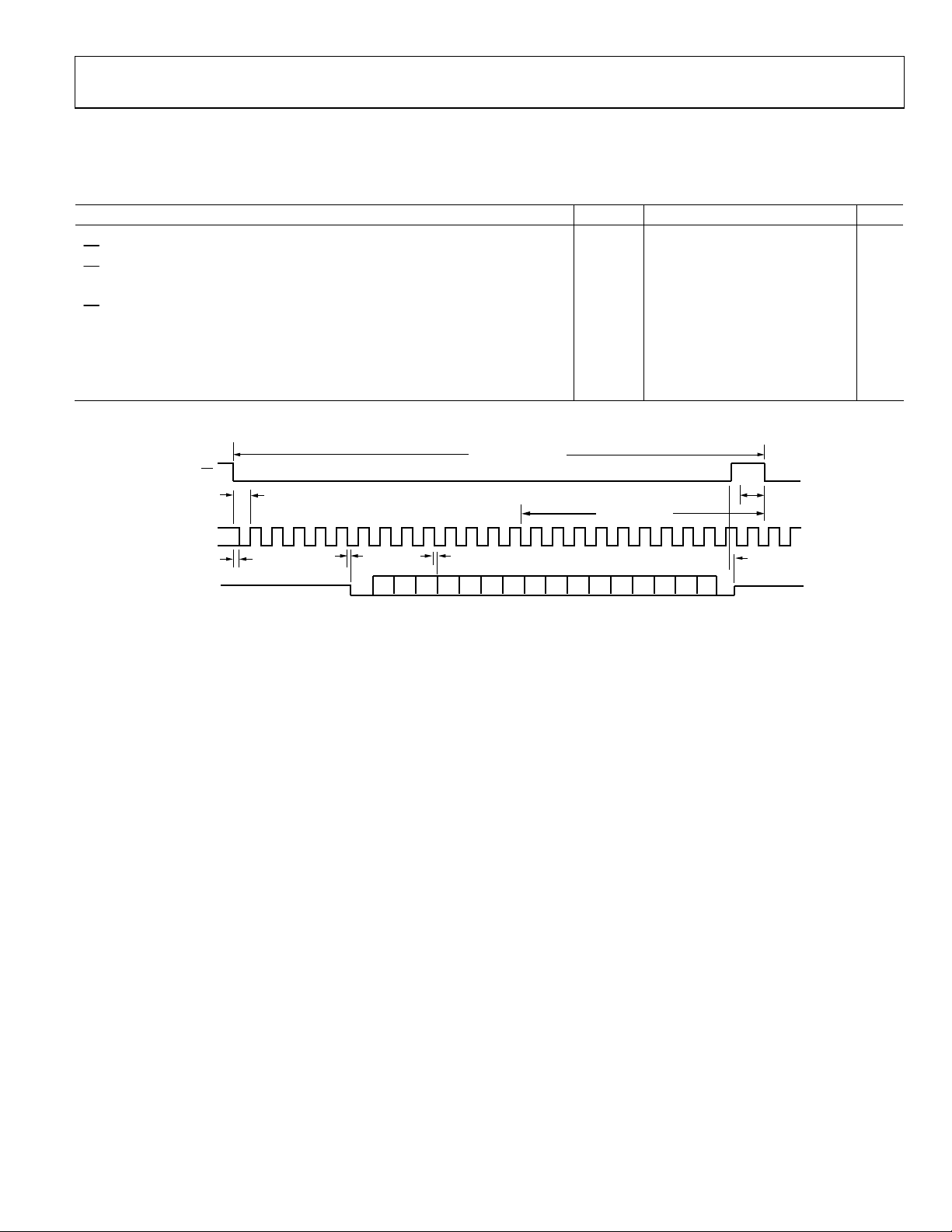
TIMING SPECIFICATIONS
VDD = 2.7 V to 5.5 V; TA = −40°C to +85°C, unless otherwise noted.
Table 5.
Parameter Symbol Min Typ Max Unit
Throughput Rate t
CS Falling to DCLOCK Low
CS Falling to DCLOCK Rising
DCLOCK Falling to Data Remains Valid t
CS Rising Edge to D
High Impedance
OUT
DCLOCK Falling to Data Valid t
Acquisition Time t
D
Fall Time t
OUT
D
Rise Time t
OUT
t
CYC
CS
t
SUCS
DCLOCK
D
OUT
145
t
CSD
Hi-Z
NOTE:
A MINIMUM OF 22 CLOCK CYCLES ARE REQUIRED FOR 16-BIT CONVERSION. SHOWN ARE 24 CLOCK CYCLES.
GOES LOW ON THE DCLOCK FALLING EDGE FOLLOWING THE LSB READING.
D
OUT
t
EN
D15 D14 D13 D12 D11 D10 D9 D8 D7 D6 D5 D4 D3 D2 D1 D0
0
(MSB) (LSB)
Figure 2. Serial Interface Ti ming
COMPLETE CYCLE
t
HDO
t
t
t
CYC
CSD
SUCS
HDO
DIS
EN
ACQ
F
R
100 kHz
0 µs
20 ns
5 16 ns
14 100 ns
16 50 ns
400 ns
11 25 ns
11 25 ns
t
ACQ
POWER DOWN
t
DIS
Hi-Z
0
04301-002
Rev. 0 | Page 5 of 16
 Loading...