3 mW, 100 kSPS,
FEATURES
Fast throughput rate: 100 kSPS
Specified for V
Low power
3 mW typ at 100 kSPS with 2.5 V supply
3.9 mW typ at 100 kSPS with 3 V supply
16.7 mW typ at 100 kSPS with 5 V supply
Wide input bandwidth
86 dB SNR at 10 kHz input frequency
Flexible power/serial clock speed management
No pipeline delays
High speed serial interface
SPI®/QSPI™/µWire/DSP compatible
Standby mode: 0.5 µA max
6-Lead SOT-23 and 8-Lead MSOP packages
APPLICATIONS
Battery-powered systems:
Personal digital assistants
Medical instruments
Mobile communications
Instrumentation and control systems
Remote data acquisition systems
High speed modems
Optical sensors
GENERAL DESCRIPTION
The AD7680 is a 16-bit, fast, low power, successive approximation
ADC. The part operates from a single 2.5 V to 5.5 V power
supply and features throughput rates up to 100 kSPS. The part
contains a low noise, wide bandwidth track-and-hold amplifier
that can handle input frequencies in excess of 7 MHz.
The conversion process and data acquisition are controlled
CS
using
and the serial clock, allowing the devices to interface
with microprocessors or DSPs. The input signal is sampled on
the falling edge of
point. There are no pipeline delays associated with the part.
of 2.5 V to 5.5 V
DD
CS
and the conversion is also initiated at this
16-Bit ADC in 6-Lead SOT-23
AD7680
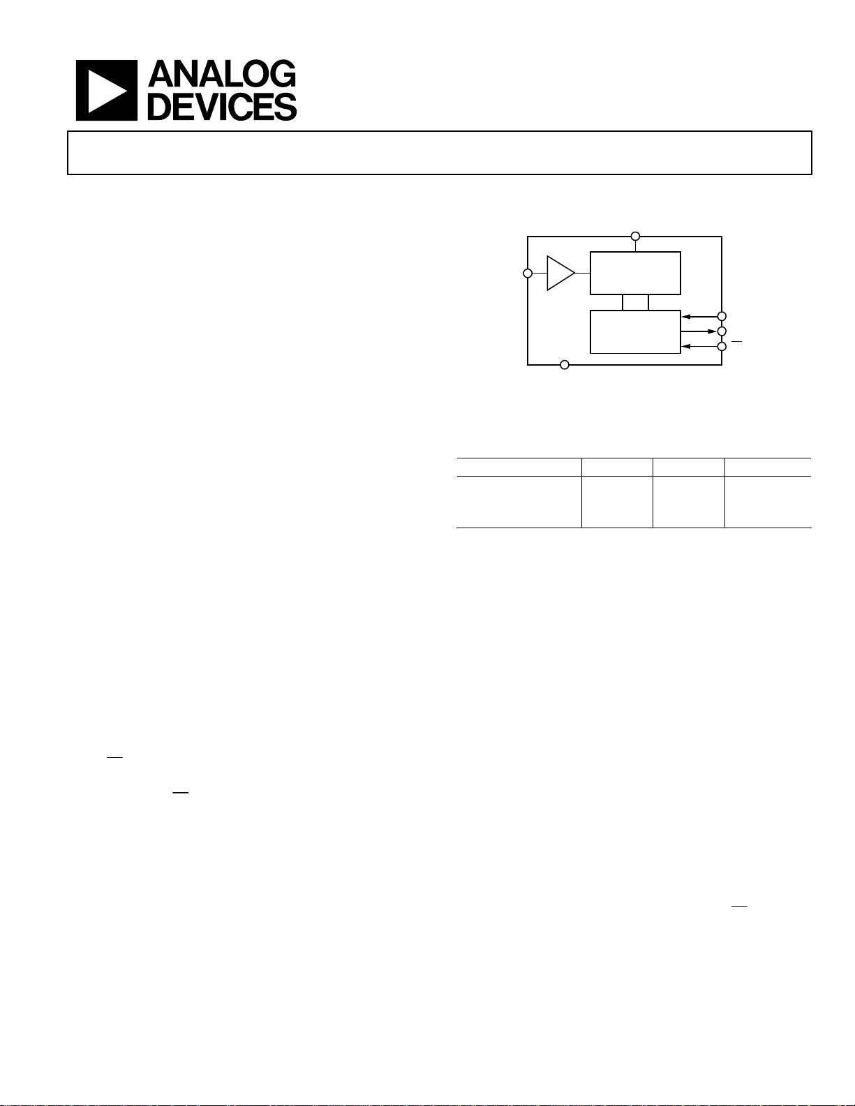
FUNCTIONAL BLOCK DIAGRAM
V
DD
GND
16-BIT SUCCESSIVE
APPROXIMATION
ADC
CONTROL
LOGIC
Figure 1.
SCLK
SDATA
CS
03643-0-001
IN
T/H
AD7680
V
Table 1. MSOP/SOT-23 16-Bit PulSAR ADC
Type/kSPS 100 kSPS 250 kSPS 500 kSPS
True Differential AD7684 AD7687 AD7688
Pseudo Differential AD7683 AD7685 AD7686
Unipolar AD7680
PRODUCT HIGHLIGHTS
1. First 16-bit ADC in a SOT-23 package.
2. High throughput with low power consumption.
3. Flexible power/serial clock speed management. The
conversion rate is determined by the serial clock, allowing
the conversion time to be reduced through the serial clock
speed increase. This allows the average power consumption
to be reduced when a power-down mode is used while not
converting. The part also features a shutdown mode to
maximize power efficiency at lower throughput rates.
Power consumption is 0.5 µA max when in shutdown.
The AD7680 uses advanced design techniques to achieve very
low power dissipation at fast throughput rates. The reference for
the part is taken internally from V
, which allows the widest
DD
dynamic input range to the ADC. Thus, the analog input range
for this part is 0 V to V
. The conversion rate is determined by
DD
the SCLK frequency.
Rev. 0
Information furnished by Analog Devices is believed to be accurate and reliable.
However, no responsibility is assumed by Analog Devices for its use, nor for any
infringements of patents or other rights of third parties that may result from its use.
Specifications subject to change without notice. No license is granted by implication
or otherwise under any patent or patent rights of Analog Devices. Trademarks and
registered trademarks are the property of their respective owners.
4. Reference derived from the power supply.
5. No pipeline delays.
This part features a standard successive approximation ADC
with accurate control of the sampling instant via a
once-off conversion control.
One Technology Way, P.O. Box 9106, Norwood, MA 02062-9106, U.S.A.
Tel: 781.329.4700 www.analog.com
Fax: 781.326.8703 © 2004 Analog Devices, Inc. All rights reserved.
CS
input and

AD7680
TABLE OF CONTENTS
Specifications..................................................................................... 3
Digital Inputs.......................................................................... 13
Timing Specifications....................................................................... 6
Absolute Maximum Ratings............................................................ 7
ESD Caution.................................................................................. 7
Pin Configurations and Function Descriptions ........................... 8
Terminology ...................................................................................... 9
Typical Performance Characteristics ........................................... 10
Circuit Information........................................................................ 12
Converter Operation.................................................................. 12
Analog Input............................................................................... 12
ADC Transfer Function................................................................. 13
Typical Connection Diagram ................................................... 13
REVISION HISTORY
Revision 0: Initial Version
Modes of Operation ....................................................................... 14
Normal Mode.............................................................................. 14
Power-Down Mode.................................................................... 15
Power vs. Throughput Rate ........................................................... 16
Serial Interface ................................................................................ 17
AD7680 to ADSP-218x.............................................................. 18
Application Hints ........................................................................... 19
Grounding and Layout .............................................................. 19
Evaluating the AD7680 Performance ...................................... 19
Outline Dimensions....................................................................... 20
Ordering Guide .......................................................................... 20
Rev. 0 | Page 2 of 20

AD7680
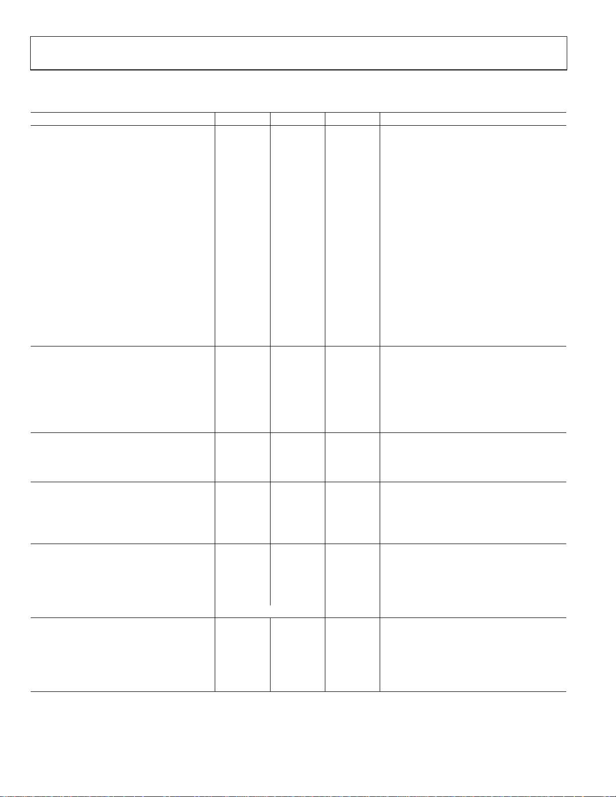
SPECIFICATIONS1
Table 2. VDD = 4.5 V to 5.5 V, f
Parameter A, B Versions1 Unit Test Conditions/Comments
DYNAMIC PERFORMANCE fIN = 10 kHz sine wave
Signal-to-Noise + Distortion (SINAD)2 83 dB min
85 dB typ
Signal-to-Noise Ratio (SNR)2 84 dB min
86 dB typ
Total Harmonic Distortion (THD)2 −97 dB typ
Peak Harmonic or Spurious Noise (SFDR)2 −95 dB typ
Intermodulation Distortion (IMD)2
Second-Order Terms −94 dB typ
Third-Order Terms −100 dB typ
Aperture Delay 20 ns max
Aperture Jitter 30 ps typ
Full Power Bandwidth 8 MHz typ @ −3 dB
2.2 MHz typ @ −0.1 dB
DC ACCURACY
No Missing Codes 15 Bits typ
Integral Nonlinearity2 ±4 LSB typ
Offset Error2 ±1.68 mV max
Gain Error2 ±0.038 % FS max
ANALOG INPUT
Input Voltage Ranges 0 to VDD V
DC Leakage Current ±0.3 µA max
Input Capacitance 30 pF typ
LOGIC INPUTS
Input High Voltage, V
Input Low Voltage, V
2.8 V min
INH
0.4 V max
INL
Input Current, IIN ±0.3 µA max Typically 10 nA, VIN = 0 V or VDD
Input Capacitance, C
2, 3
10 pF max
IN
LOGIC OUTPUTS
Output High Voltage, VOH VDD − 0.2 V min I
Output Low Voltage, VOL 0.4 V max I
Floating-State Leakage Current ±0.3 µA max
Floating-State Output Capacitance
Output Coding Straight (Natural) Binary
CONVERSION RATE
Conversion Time 8 µs max 20 SCLK cycles with SCLK at 2.5 MHz
9.6 µs max 24 SCLK cycles with SCLK at 2.5 MHz
Track-and-Hold Acquisition Time 1.5 µs max
400 ns max Sine wave input ≤ 10 kHz
Throughput Rate 100 kSPS See the Serial Interface section
POWER REQUIREMENTS
VDD 4.5/5.5 V min/V max
IDD Digital I/PS = 0 V or VDD
Normal Mode (Static) 5.2 mA max SCLK on or off. VDD = 5.5 V
Normal Mode (Operational) 4.8 mA max f
Full Power-Down Mode 0.5 µA max SCLK on or off. VDD = 5.5 V
Power Dissipation4 V
Normal Mode (Operational) 26.4 mW max f
Full Power-Down 2.75 µW max
1
Temperature range as follows: B Version: −40°C to +85°C.
2
See the Terminology section.
3
Sample tested during initial release to ensure compliance.
4
See the Power vs. Throughput Rate section.
= 2.5 MHz, f
SCLK
2, 3
10 pF max
= 100 kSPS, unless otherwise noted; TA = T
SAMPLE
to T
MIN
= 200 µA
SOURCE
= 200 µA
SINK
= 100 kSPS. VDD = 5.5 V; 3.3 mA typ
SAMPLE
= 5.5 V
DD
= 100 kSPS
SAMPLE
, unless otherwise noted
MAX
Rev. 0 | Page 3 of 20

AD7680
SPECIFICATIONS1
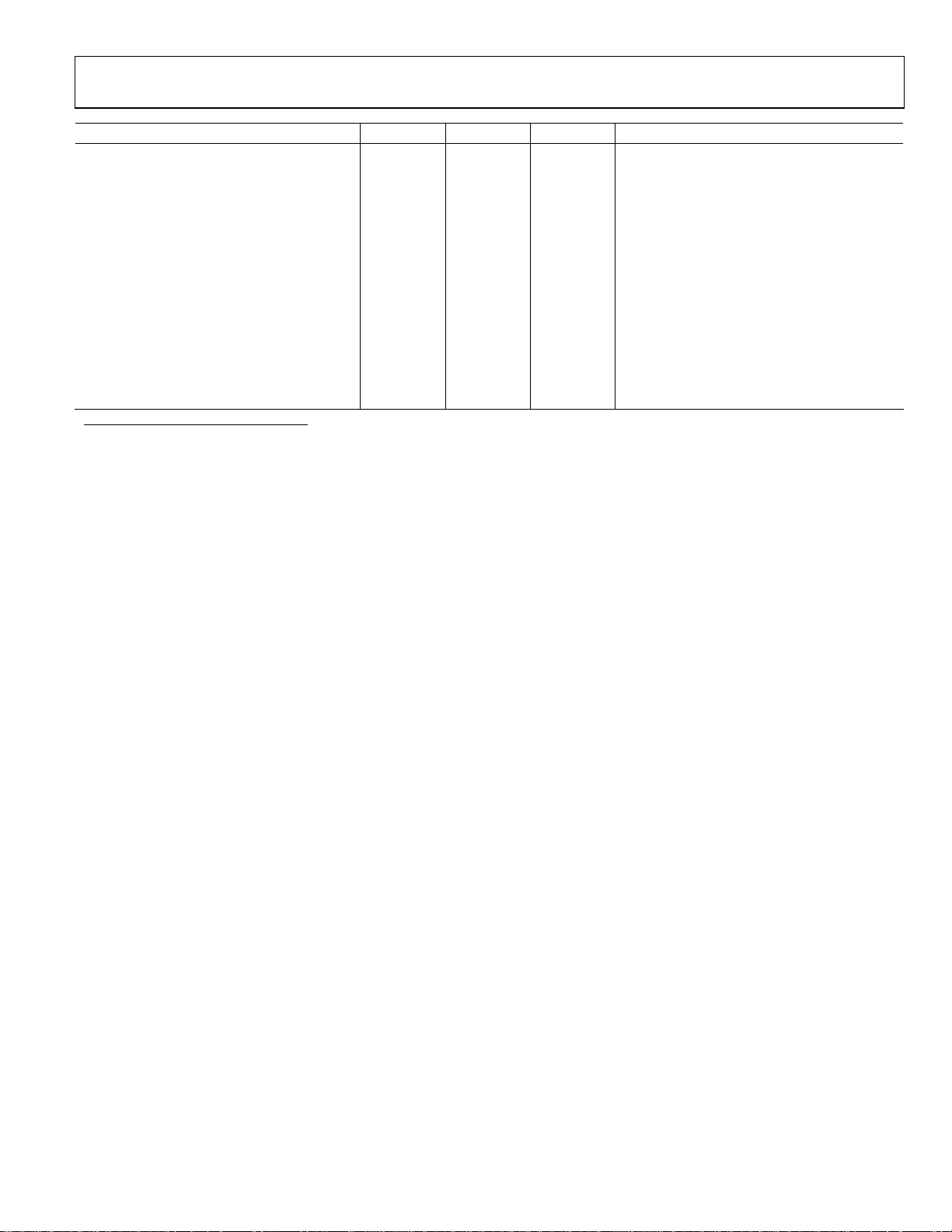
Table 3. VDD = 2.5 V to 4.096 V, f
Parameter A Version1 B Version1 Unit Test Conditions/Comments
DYNAMIC PERFORMANCE fIN = 10 kHz sine wave
Signal-to-Noise + Distortion (SINAD)2 83 83 dB min VDD = 4.096 V
82 82 dB min VDD = 2.5 V to 3.6 V
86 86 dB typ
Signal-to-Noise Ratio (SNR)2 84 84 dB min VDD = 4.096 V
83 83 dB min VDD = 2.5 V to 3.6 V
86 86 dB typ
Total Harmonic Distortion (THD) 2 −98 −98 dB typ
Peak Harmonic or Spurious Noise (SFDR)2 −95 −99 dB typ
Intermodulation Distortion (IMD)2
Second-Order Terms −94 −94 dB typ
Third-Order Terms −100 −100 dB typ
Aperture Delay 20 10 ns max
Aperture Jitter 30 30 ps typ
Full Power Bandwidth 7 7 MHz typ @ −3 dB; VDD = 4.096 V
5 5 MHz typ @ −3 dB; VDD = 2.5 V to 3.6 V
2 2 MHz typ @ −0.1 dB; VDD = 4.096 V
1.6 1.6 MHz typ @ −0.1 dB; VDD = 2.5 V to 3.6 V
DC ACCURACY
No Missing Codes 14 15 Bits min
Integral Nonlinearity2 ±3.5 ±3.5 LSB max VDD = 4.096 V
±3 ±3 LSB max VDD = 2.5 V to 3.6 V
Offset Error2 ±1.25 ±1.25 mV max VDD = 4.096 V
±1.098 ±1.098 mV max VDD = 2.5 V to 3.6 V
Gain Error2 ±0.038 ±0.038 % FS max
ANALOG INPUT
Input Voltage Ranges 0 to V
DC Leakage Current ±0.3 ±0.3 µA max
Input Capacitance 30 30 pF typ
LOGIC INPUTS
Input High Voltage, V
Input Low Voltage, V
Input Current, I
IN
Input Capacitance, C
2.4 2.4 V min
INH
0.4 0.4 V max
INL
±0.3 ±0.3 µA max Typically 10 nA, VIN = 0 V or VDD
2, 3
10 10 pF max
IN
LOGIC OUTPUTS
Output High Voltage, V
V
OH
Output Low Voltage, VOL 0.4 0.4 V max I
Floating-State Leakage Current ±0.3 ±0.3 µA max
Floating-State Output Capacitance
Output Coding Straight (Natural) Binary
CONVERSION RATE
Conversion Time 8 8 µs max 20 SCLK cycles with SCLK at 2.5 MHz
9.6 9.6 µs max 24 SCLK cycles with SCLK at 2.5 MHz
Track-and-Hold Acquisition Time 1.5 1.5 µs max Full-scale step input
400 400 ns max Sine wave input ≤ 10 kHz
Throughput Rate 100 100 kSPS See the Serial Interface section
= 2.5 MHz, f
SCLK
2, 3
10 10 pF max
= 100 kSPS, unless otherwise noted; TA = T
SAMPLE
0 to V
DD
− 0.2 VDD − 0.2 V min I
DD
V
DD
MIN
= 200 µA
SOURCE
= 200 µA
SINK
to T
, unless otherwise noted.
MAX
Rev. 0 | Page 4 of 20

AD7680
Parameter A Version1 B Version1 Unit Test Conditions/Comments
POWER REQUIREMENTS
VDD 2.5/4.096 2.5/4.096 V min/max
IDD Digital I/Ps = 0 V or VDD
Normal Mode (Static) 2.8 2.8 mA max SCLK on or off; VDD = 4.096 V
2 2 mA max SCLK on or off; VDD = 3.6 V
Normal Mode (Operational) 2.6 2.6 mA max f
1.9 1.9 mA max f
Full Power-Down Mode 0.3 0.3 µA max SCLK on or off
Power Dissipation4
Normal Mode (Operational) 10.65 10.65 mW max f
6.84 6.84 mW max f
3 3 mW typ VDD = 2.5 V
Full Power-Down 1.23 1.23 µW max VDD = 4.096V
1.08 1.08 µW max VDD = 3.6 V
1
Temperature range as follows: A, B Versions: −40°C to +85°C.
2
See the Terminology section.
3
Sample tested during initial release to ensure compliance.
4
See the Power vs. Throughput Rate section.
= 100 kSPS; VDD = 4.096 V; 1.75 mA typ
SAMPLE
= 100 kSPS; VDD = 3.6 V; 1.29 mA typ
SAMPLE
= 100 kSPS; VDD = 4.096 V
SAMPLE
= 100 kSPS; VDD = 3.6 V
SAMPLE
Rev. 0 | Page 5 of 20

AD7680
TIMING SPECIFICATIONS1
Table 4. VDD = 2.5 V to 5.5 V; TA = T
Limit at T
MIN
, T
MAX
Parameter 3 V 5 V Unit Description
2
f
250 250 kHz min
SCLK
2.5 2.5 MHz max
t
20 × t
CONVERT
t
100 100 ns min Minimum quiet time required between bus relinquish and start of next conversion
QUIET
20 × t
SCLK
t1 10 10 ns min
t2 10 10 ns min
3
t
48 35 ns max
3
3
t
120 80 ns max Data access time after SCLK falling edge
4
t5 0.4 t
t6 0.4 t
0.4 t
SCLK
0.4 t
SCLK
SCLK
SCLK
t7 10 10 ns min SCLK to data valid hold time
4
t
45 35 ns max SCLK falling edge to SDATA high impedance
8
5
t
1 1 µs typ Power up time from full power-down
POWER-UP
1
Sample tested during initial release to ensure compliance. All input signals are specified with tr = tf = 5 ns (10% to 90% of VDD) and timed from a voltage level of 1.6 V.
2
Mark/space ratio for the SCLK input is 40/60 to 60/40.
3
Measured with the load circuit of Figure 2 and defined as the time required for the output to cross 0.8 V or 2.0 V.
4
t8 is derived form the measured time taken by the data outputs to change 0.5 V when loaded with the circuit of Figure 2. The measured number is then extrapolated
back to remove the effects of charging or discharging the 50 pF capacitor. This means that the time, t
time of the part and is independent of the bus loading.
5
See Power vs. Throughput Rate section.
MIN
to T
, unless otherwise noted.
MAX
min
SCLK
Minimum
CS
Delay from
CS
pulse width
to SCLK setup time
CS
until SDATA three-state disabled
ns min SCLK low pulse width
ns min SCLK high pulse width
, quoted in the timing characteristics is the true bus relinquish
8
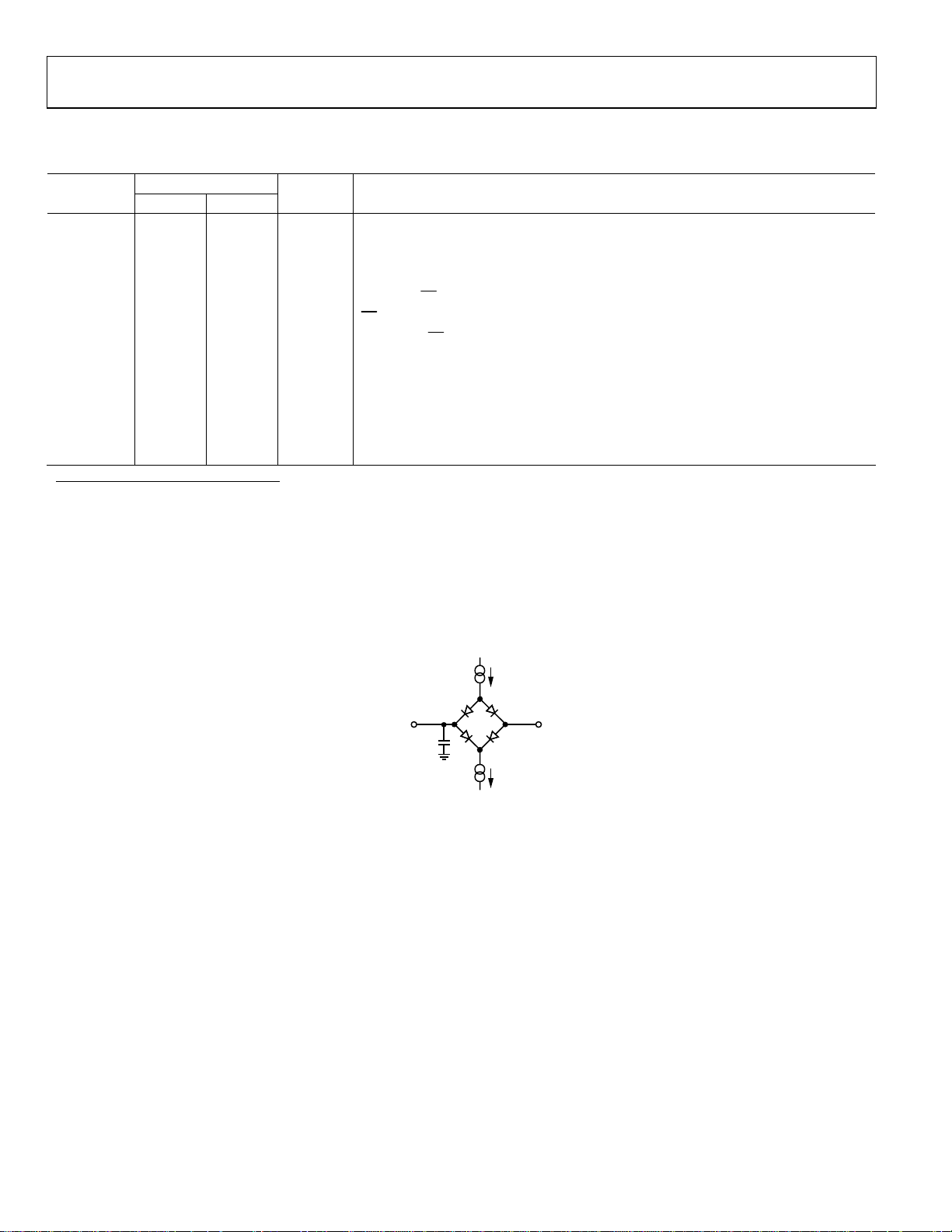
200µAI
TO OUTPUT
PIN
C
L
50pF
200µAI
Figure 2. Load Circuit for Digital Output Timing Specification
OL
1.6V
OH
03643-0-002
Rev. 0 | Page 6 of 20
 Loading...