ANALOG DEVICES AD7665 Service Manual
现货库存、技术资料、百科信息、热点资讯,精彩尽在鼎好!
a
FEATURES
Throughput:
570 kSPS (Warp Mode)
500 kSPS (Normal Mode)
INL: 2.5 LSB Max (0.0038% of Full Scale)
16-Bit Resolution with No Missing Codes
S/(N+D): 90 dB Typ @ 180 kHz
THD: –100 dB Typ @ 180 kHz
Analog Input Voltage Ranges:
Bipolar: 10 V, 5 V, 2.5 V
Unipolar: 0 V to 10 V, 0 V to 5 V, 0 V to 2.5 V
Both AC and DC Specifications
No Pipeline Delay
Parallel (8/16 Bits) and Serial 5 V/3 V Interface
Single 5 V Supply Operation
Power Dissipation
64 mW Typical
15 W @ 100 SPS
Power-Down Mode: 7 W Max
Package: 48-Lead Quad Flatpack (LQFP)
Pin-to-Pin Compatible Upgrade of the AD7664/AD7663
16-Bit, 570 kSPS CMOS ADC
AD7665*
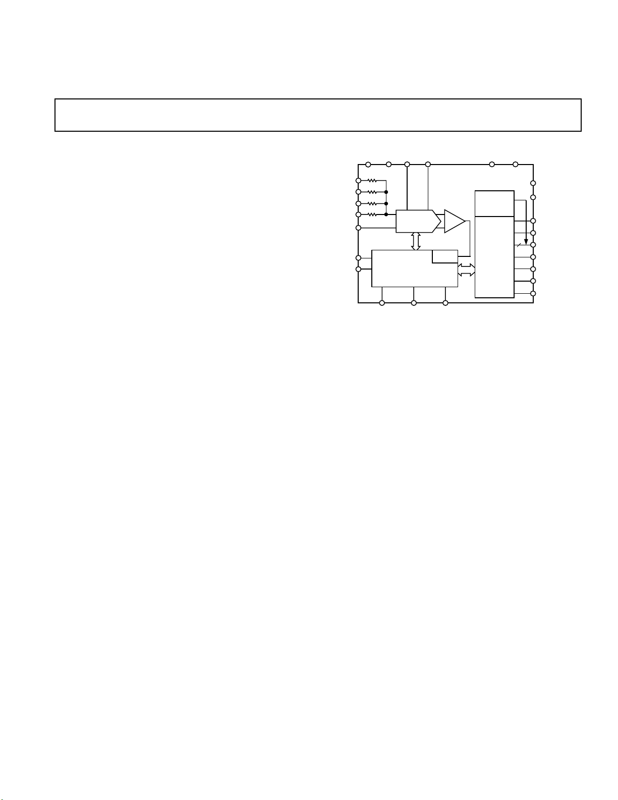
FUNCTIONAL BLOCK DIAGRAM
DGNDDVDDAVDD AGND REF REFGND
PD
4R
4R
2R
R
SWITCHED
CAP DAC
CONTROL LOGIC AND
CALIBRATION CIRCUITRY
AD7665
CLOCK
CNVSTIMPULSEWARP
SERIAL
PORT
PARALLEL
INTERFACE
16
IND(4R)
INC(4R)
INB(2R)
INA(R)
INGND
RESET
OVDD
OGND
SER/PAR
BUSY
DATA[15:0]
CS
RD
OB/2C
BYTESWAP
APPLICATIONS
Data Acquisition
Communication
Instrumentation
Spectrum Analysis
Medical Instruments
Process Control
GENERAL DESCRIPTION
The AD7665 is a 16-bit, 570 kSPS, charge redistribution SAR,
analog-to-digital converter that operates from a single 5 V power
supply. It contains a high-speed 16-bit sampling ADC, a resistor
input scaler which allows various input ranges, an internal conversion clock, error correction circuits, and both serial and
parallel system interface ports.
The AD7665 is hardware factory-calibrated and is comprehensively tested to ensure such ac parameters as signal-to-noise ratio
(SNR) and total harmonic distortion (THD), in addition to the
more traditional dc parameters of gain, offset, and linearity.
It features a very high sampling rate mode (Warp) and, for
asynchronous conversion rate applications, a fast mode (Normal) and, for low power applications, a reduced power mode
(Impulse) where the power is scaled with the throughput. It is
fabricated using Analog Devices’ high-performance, 0.6 micron
CMOS process and is available in a 48-lead LQFP with operation specified from –40°C to +85°C.
PRODUCT HIGHLIGHTS
1. Fast Throughput
The AD7665 is a very high speed (570 kSPS in Warp mode
and 500 kSPS in Normal mode), charge redistribution,
16-bit SAR ADC.
2. Single Supply Operation
The AD7665 operates from a single 5 V supply, dissipates
only 64 mW typical, even lower when a reduced throughput
is used with the reduced power mode (Impulse) and a powerdown mode.
3. Superior INL
The AD7665 has a maximum integral nonlinearity of 2.5 LSB
with no missing 16-bit code.
4. Serial or Parallel Interface
Versatile parallel (8 or 16 bits) or 2-wire serial interface
arrangement compatible with both 3 V or 5 V logic.
*Patent pending.
REV. 0
Information furnished by Analog Devices is believed to be accurate and
reliable. However, no responsibility is assumed by Analog Devices for its
use, nor for any infringements of patents or other rights of third parties that
may result from its use. No license is granted by implication or otherwise
under any patent or patent rights of Analog Devices.
One Technology Way, P.O. Box 9106, Norwood, MA 02062-9106, U.S.A.
Tel: 781/329-4700 www.analog.com
Fax: 781/326-8703 © Analog Devices, Inc., 2001

AD7665–SPECIFICATIONS
(–40C to +85C, AVDD = DVDD = 5 V, OVDD = 2.7 V to 5.25 V, unless otherwise noted.)
Parameter Conditions Min Typ Max Unit
RESOLUTION 16 Bits
ANALOG INPUT
Voltage Range V
Common-Mode Input Voltage V
Analog Input CMRR f
– V
IND
INGND
INGND
= 180 kHz 62 dB
IN
±4 REF, 0 V to 4 REF, ± 2 REF (See Table I)
–0.1 +0.5 V
Input Impedance See Table I
THROUGHPUT SPEED
Complete Cycle In Warp Mode 1.75 µs
Throughput Rate In Warp Mode 1 570 kSPS
Time Between Conversions In Warp Mode 1 ms
Complete Cycle In Normal Mode 2 µs
Throughput Rate In Normal Mode 0 500 kSPS
Complete Cycle In Impulse Mode 2.25 µs
Throughput Rate In Impulse Mode 0 444 kSPS
DC ACCURACY
Integral Linearity Error –2.5 +2.5 LSB
1
No Missing Codes 16 Bits
Transition Noise 0.7 LSB
Bipolar Zero Error
2
, T
MIN
to T
MAX
±5 V Range, Normal or –25 +25 LSB
Impulse Modes
2
Bipolar Full-Scale Error
Unipolar Zero Error
2
, T
, T
MIN
Unipolar Full-Scale Error
2
, T
MIN
to T
MIN
to T
MAX
to T
MAX
Other Range or Mode –0.06 +0.06 % of FSR
–0.25 +0.25 % of FSR
–0.18 +0.18 % of FSR
MAX
–0.38 +0.38 % of FSR
Power Supply Sensitivity AVDD = 5 V ± 5% ±9.5 LSB
AC ACCURACY
Signal-to-Noise fIN = 10 kHz 89 90 dB
3
fIN = 180 kHz 90 dB
Spurious Free Dynamic Range f
Total Harmonic Distortion f
Signal-to-(Noise+Distortion) f
= 180 kHz 100 dB
IN
= 180 kHz –100 dB
IN
= 10 kHz 88.5 90 dB
IN
= 180 kHz, –60 dB Input 30 dB
f
IN
–3 dB Input Bandwidth 3.6 MHz
SAMPLING DYNAMICS
Aperture Delay 2ns
Aperture Jitter 5 ps rms
Transient Response Full-Scale Step 1 µs
REFERENCE
External Reference Voltage Range 2.3 2.5 2.7 V
External Reference Current Drain 570 kSPS Throughput 114 µA
DIGITAL INPUTS
Logic Levels
V
IL
V
IH
I
IL
I
IH
–0.3 +0.8 V
+2.0 DVDD + 0.3 V
–1 +1 µA
–1 +1 µA
DIGITAL OUTPUTS
Data Format Parallel or Serial 16-Bit
Pipeline Delay Conversion Results Available Immediately
after Completed Conversion
I
V
OL
V
OH
= 1.6 mA 0.4 V
SINK
I
= –570 µA OVDD – 0.6 V
SOURCE
POWER SUPPLIES
Specified Performance
AVDD 4.75 5 5.25 V
DVDD 4.75 5 5.25 V
OVDD 2.7 5.25 V
Operating Current
AVDD 14 mA
5
DVDD
5
OVDD
4
570 kSPS Throughput
4.5 mA
20 µA
–2–
REV. 0
AD7665
Parameter Conditions Min Typ Max Unit
POWER SUPPLIES (Continued)
Power Dissipation
In Power-Down Mode
TEMPERATURE RANGE
Specified Performance T
NOTES
1
LSB means Least Significant Bit. With the ± 5 V input range, one LSB is 152.588 µV.
2
See Definition of Specifications section. These specifications do not include the error contribution from the external reference.
3
All specifications in dB are referred to a full-scale input FS. Tested with an input signal at 0.5 dB below full scale unless otherwise specified.
4
In warp mode.
5
Tested in parallel reading mode.
6
Tested with the 0 V to 5 V range and VIN – V
7
In impulse mode.
8
With OVDD below DVDD + 0.3 V and all digital inputs forced to OVDD or OGND respect ively.
9
Contact factory for extended temperature range.
Specifications subject to change without notice.
5, 6
444 kSPS Throughput
100 SPS Throughput
8
9
570 kSPS Throughput
to T
MIN
= 0 V. See Power Dissipation section.
INGND
MAX
7
7
4
64 74 mW
15 µW
93 107 mW
7 µW
–40 +85 °C
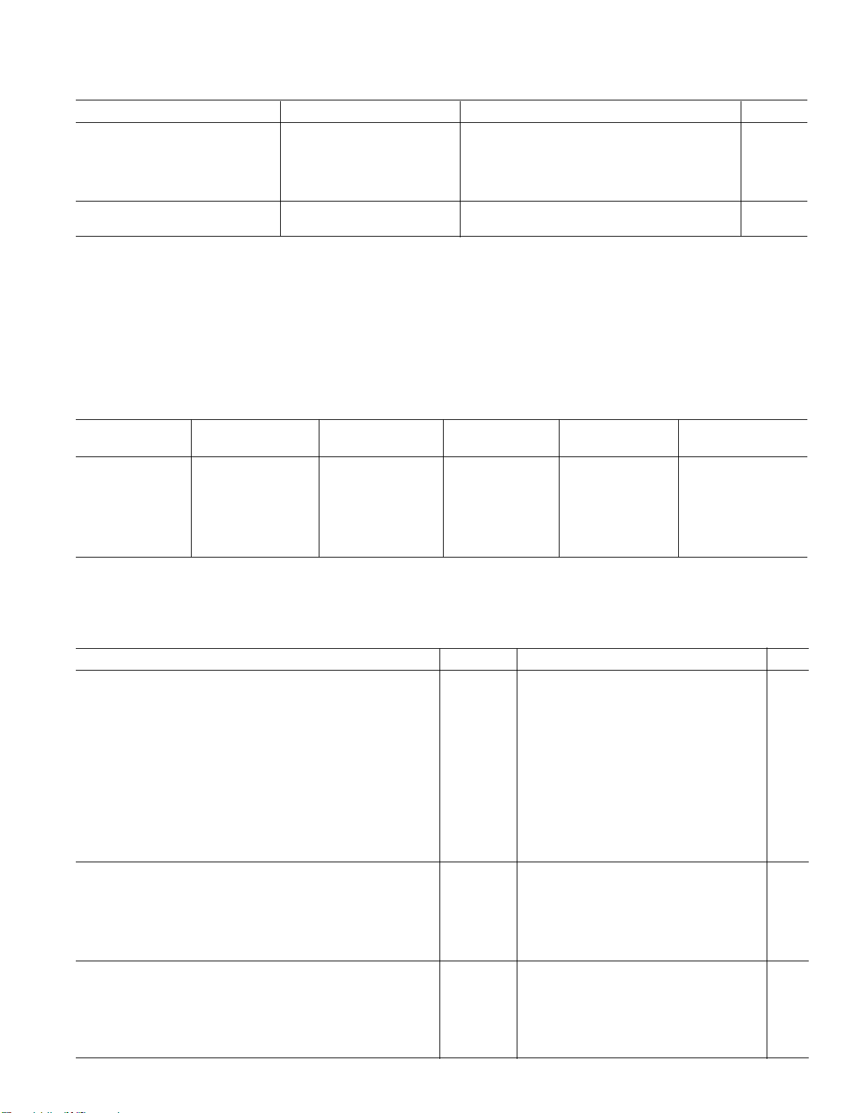
Table I. Analog Input Configuration
Input Voltage Input
Range IND (4R) INC (4R) INB (2R) INA (R) Impedance
±4 REF V
±2 REF V
±REF V
0 V to 4 REF V
0 V to 2 REF V
0 V to REF V
NOTES
1
Typical analog input impedance.
2
For this range the input is high impedance.
IN
IN
IN
IN
IN
IN
TIMING SPECIFICATIONS
(–40C to +85C, AVDD = DVDD = 5 V, OVDD = 2.7 V to 5.25 V, unless otherwise noted.)
INGND INGND REF 5.85 kΩ
V
IN
V
IN
V
IN
V
IN
V
IN
INGND REF 3.41 kΩ
V
IN
REF 2.56 kΩ
INGND INGND 3.41 kΩ
V
IN
V
IN
INGND 2.56 kΩ
V
IN
Note 2
Symbol Min Typ Max Unit
Refer to Figures 11 and 12
Convert Pulsewidth t
Time Between Conversions t
1
2
5ns
1.75/2/2.25 Note 1 µs
(Warp Mode/Normal Mode/Impulse Mode)
CNVST LOW to BUSY HIGH Delay t
BUSY HIGH All Modes Except in Master Serial Read after t
3
4
30 ns
0.75/1/1.25 µs
Convert Mode (Warp Mode/Normal Mode/Impulse Mode)
Aperture Delay t
End of Conversion to BUSY LOW Delay t
Conversion Time (Warp Mode/Normal Mode/Impulse Mode) t
Acquisition Time t
RESET Pulsewidth t
5
6
7
8
9
10 ns
1 µs
10 ns
2ns
0.75/1/1.25 µs
Refer to Figures 13, 14, and 15 (Parallel Interface Modes)
CNVST LOW to DATA Valid Delay t
10
0.75/1/1.25 µs
(Warp Mode/Normal Mode/Impulse Mode)
DATA Valid to BUSY LOW Delay t
Bus Access Request to DATA Valid t
Bus Relinquish Time t
Refer to Figures 17 and 18 (Master Serial Interface Modes)
2
CS LOW to SYNC Valid Delay t
CS LOW to Internal SCLK Valid Delay t
CS LOW to SDOUT Delay t
CNVST LOW to SYNC Delay (Read During Convert) t
11
12
13
14
15
16
17
20 ns
40 ns
515ns
10 ns
10 ns
10 ns
25/275/525 ns
(Warp Mode/Normal Mode/Impulse Mode)
1
REV. 0
–3–
AD7665
TIMING SPECIFICATIONS
(Continued)
Symbol Min Typ Max Unit
SYNC Asserted to SCLK First Edge Delay
Internal SCLK Period
Internal SCLK HIGH
Internal SCLK LOW
SDOUT Valid Setup Time
SDOUT Valid Hold Time
SCLK Last Edge to SYNC Delay
3
3
3
3
3
3
CS HIGH to SYNC HI-Z t
CS HIGH to Internal SCLK HI-Z t
CS HIGH to SDOUT HI-Z t
BUSY HIGH in Master Serial Read After Convert
CNVST LOW to SYNC Asserted Delay t
3
3
t
18
t
19
t
20
t
21
t
22
t
23
t
24
25
26
27
t
28
29
4ns
25 40 ns
15 ns
9.5 ns
4.5 ns
2ns
3
Master Serial Read after Convert
SYNC Deasserted to BUSY LOW Delay t
30
Refer to Figures 19 and 21 (Slave Serial Interface Modes)
External SCLK Setup Time t
External SCLK Active Edge to SDOUT Delay t
SDIN Setup Time t
SDIN Hold Time t
External SCLK Period t
External SCLK HIGH t
External SCLK LOW t
NOTES
1
In warp mode only, the maximum time between conversions is 1 ms, otherwise, there is no required maximum time.
2
In serial interface modes, the SYNC, SCLK, and SDOUT timings are defined with a maximum load C
3
In serial master read during convert mode. See Table II.
Specifications subject to change without notice.
31
32
33
34
35
36
37
5ns
316ns
5ns
5ns
25 ns
10 ns
10 ns
of 10 pF; otherwise, the load is 60 pF maximum.
L
10 ns
10 ns
10 ns
See Table II µs
0.75/1/1.25 µs
25 ns
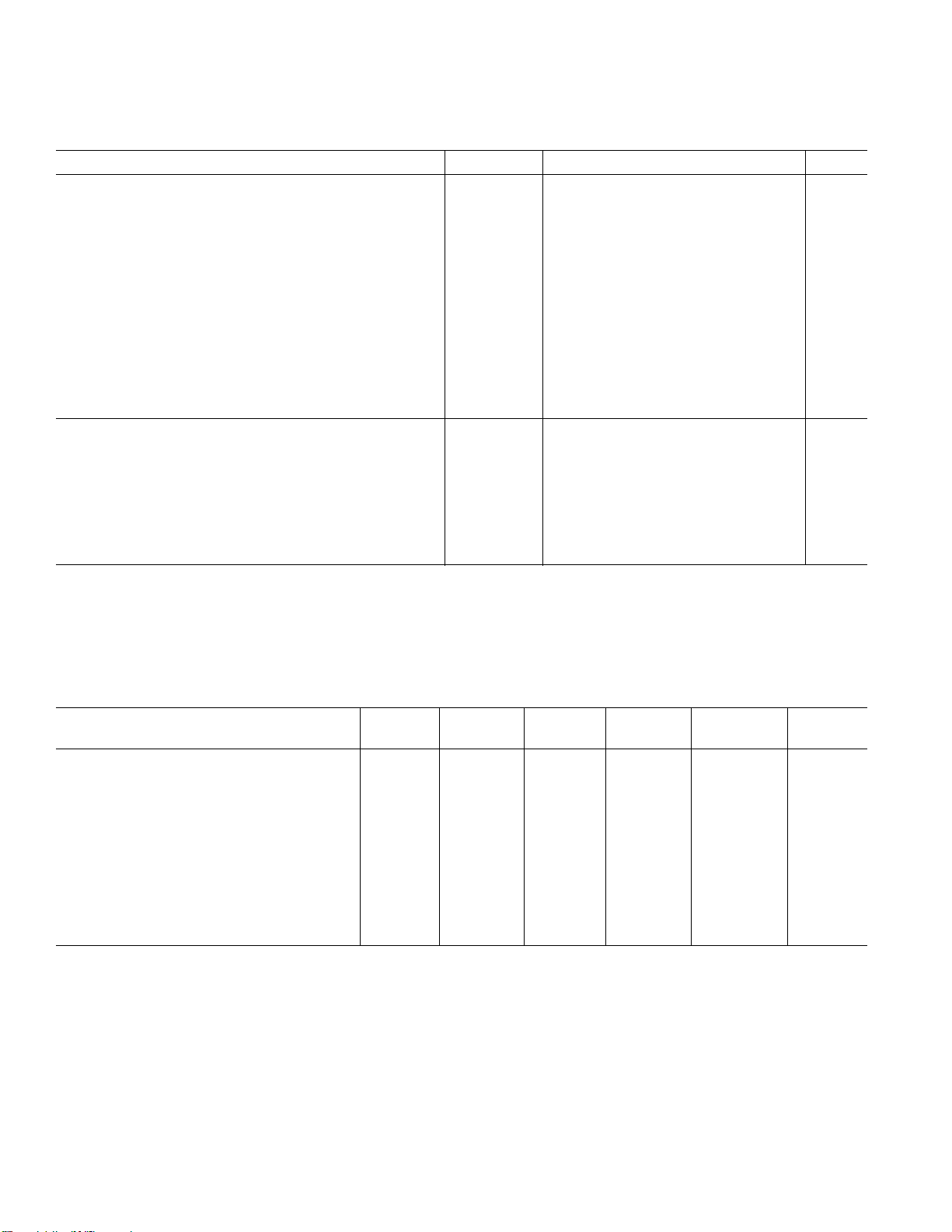
Table II. Serial Clock Timings in Master Read after Convert
DIVSCLK[1] 0011
DIVSCLK[0] 0101 Unit
SYNC to SCLK First Edge Delay Minimum t
Internal SCLK Period Minimum t
Internal SCLK Period Maximum t
Internal SCLK HIGH Minimum t
Internal SCLK LOW Minimum t
SDOUT Valid Setup Time Minimum t
SDOUT Valid Hold Time Minimum t
SCLK Last Edge to SYNC Delay Minimum t
BUSY HIGH Width Maximum (Warp) t
BUSY HIGH Width Maximum (Normal) t
BUSY HIGH Width Maximum (Impulse) t
18
19
19
20
21
22
23
24
28
28
28
4 202020 ns
25 50 100 200 ns
40 70 140 280 ns
15 25 50 100 ns
9.5 24 49 99 ns
4.5 22 22 22 ns
243090 ns
3 60 140 300 ns
1.5 2 3 5.25 µs
1.75 2.25 3.25 5.5 µs
2 2.5 3.5 5.75 µs
–4–
REV. 0
WARNING!
ESD SENSITIVE DEVICE
1.6mA I
36
35
34
33
32
31
30
29
28
27
26
25
13 14
15 16 17 18 19 20 21 22 23 24
1
2
3
4
5
6
7
8
9
10
11
12
48
47 46 45 44 39 38 3743 42 41 40
PIN 1
IDENTIFIER
TOP VIEW
(Not to Scale)
AGND
CNVST
PD
RESET
CS
RD
DGND
AGND
AVDD
NC
BYTESWAP
OB/2C
WARP
IMPULSE
NC = NO CONNECT
SER/PAR
D0
D1
D2/DIVSCLK[0]
BUSY
D15
D14
D13
AD7665
D3/DIVSCLK[1]
D12
D4/EXT/INT
D5/INVSYNC
D6/INVSCLK
D7/RDC/SDIN
OGND
OVDD
DVDD
DGND
D8/SDOUT
D9/SCLK
D10/SYNC
D11/RDERROR
NCNCNCNCNC
IND(4R)
INC(4R)
INB(2R)
INA(R)
INGND
REFGND
REF
AD7665
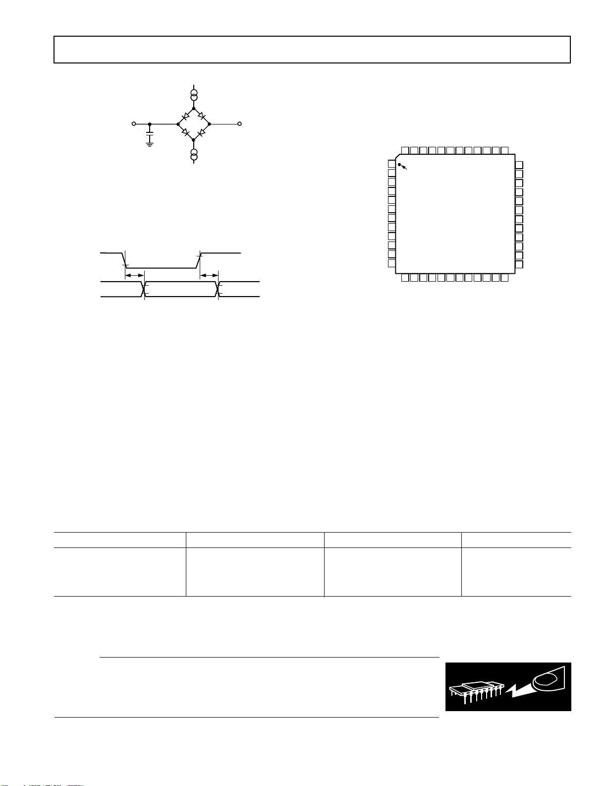
PIN CONFIGURATION
OL
48-Lead LQFP
(ST-48)
TO OUTPUT
PIN
NOTE:
1
IN SERIAL INTERFACE MODES, THE SYNC, SCLK, AND
SDOUT TIMINGS ARE DEFINED WITH A MAXIMUM LOAD
OF 10pF; OTHERWISE, THE LOAD IS 60pF MAXIMUM.
C
L
C
L
60pF
1
500A
I
OH
1.4V
Figure 1. Load Circuit for Digital Interface Timing, SDOUT,
SYNC, SCLK Outputs, C
0.8V
t
DELAY
= 10 pF
L
2V
t
DELAY
0.8V 0.8V
2V2V
Figure 2. Voltage Reference Levels for Timing
ABSOLUTE MAXIMUM RATINGS
Analog Inputs
2
IND
, INC2, INB2 . . . . . . . . . . . . . . . . . . . –11 V to +30 V
1
INA, REF, INGND, REFGND
. . . . . . . . . . . . . . . . . . . . AGND – 0.3 V to AVDD + 0.3 V
Ground Voltage Differences
AGND, DGND, OGND . . . . . . . . . . . . . . . . . . . . . ±0.3 V
Supply Voltages
AVDD, DVDD, OVDD . . . . . . . . . . . . . . . . . . . . . . . . . 7 V
AVDD to DVDD,
AVDD to OVDD . . . . . . . . . . . . . ±7 V
DVDD to OVDD . . . . . . . . . . . . . . . . . . . . . . . . . . . . ± 7 V
Digital Inputs . . . . . . . . . . . . . . . –0.3 V to DVDD + 0.3 V
Internal Power Dissipation
3
. . . . . . . . . . . . . . . . . . . 700 mW
Junction Temperature . . . . . . . . . . . . . . . . . . . . . . . . . 150°C
Storage Temperature Range . . . . . . . . . . . . –65°C to +150°C
Lead Temperature Range
(Soldering 10 sec) . . . . . . . . . . . . . . . . . . . . . . . . . . 300°C
NOTES
1
Stresses above those listed under Absolute Maximum Ratings may cause perma-
nent damage to the device. This is a stress rating only; functional operation of the
device at these or any other conditions above those indicated in the operational
section of this specification is not implied. Exposure to absolute maximum rating
conditions for extended periods may affect device reliability.
2
See Analog Input section.
3
Specification is for device in free air: 48-Lead LQFP: θJA = 91°C/W, θJC = 30°C/W.
ORDERING GUIDE
Model Temperature Range Package Description Package Option
AD7665AST –40°C to +85°C Quad Flatpack (LQFP) ST-48
AD7665ASTRL –40°C to +85°C Quad Flatpack (LQFP) ST-48
EVAL-AD7665CB
EVAL-CONTROL BRD2
NOTES
1
This board can be used as a stand-alone evaluation board or in conjunction with the EVAL-CONTROL BRD2 for evaluation/demonstration purposes.
2
This board allows a PC to control and communicate with all Analog Devices evaluation boards ending in the CB designators.
CAUTION
ESD (electrostatic discharge) sensitive device. Electrostatic charges as high as 4000 V readily
accumulate on the human body and test equipment and can discharge without detection. Although
the AD7665 features proprietary ESD protection circuitry, permanent damage may occur on
devices subjected to high-energy electrostatic discharges. Therefore, proper ESD precautions are
recommended to avoid performance degradation or loss of functionality.
REV. 0
1
2
Evaluation Board
Controller Board
–5–

AD7665
PIN FUNCTION DESCRIPTIONS
Pin
No. Mnemonic Type Description
1 AGND P Analog Power Ground Pin.
2 AVDD P Input Analog Power Pin. Nominally 5 V.
3, 44–48 NC No Connect.
4 BYTESWAP Parallel Mode Selection (8-/16-Bit). When LOW, the LSB is output on D[7:0] and the MSB
is output on D[15:8]. When HIGH, the LSB is output on D[15:8] and the MSB is output on
D[7:0].
5OB/2C DI Straight Binary/Binary Two’s Complement. When OB/2C is HIGH, the digital output is
straight binary; when LOW, the MSB is inverted, resulting in a two’s complement output
from its internal shift register.
6 WARP DI Mode Selection. When HIGH and IMPULSE LOW, this input selects the fastest mode, the
maximum throughput is achievable, and a minimum conversion rate must be applied in order
to guarantee full specified accuracy. When LOW, full accuracy is maintained independent of
the minimum conversion rate.
7 IMPULSE DI Mode Selection. When HIGH and WARP LOW, this input selects a reduced power mode. In
this mode, the power dissipation is approximately proportional to the sampling rate.
8 SER/PAR DI Serial/Parallel Selection Input. When LOW, the parallel port is selected; when HIGH, the
serial interface mode is selected and some bits of the DATA bus are used as a serial port.
9, 10 DATA[0:1] DO Bit 0 and Bit 1 of the Parallel Port Data Output Bus. When SER/PAR is HIGH, these outputs
are in high impedance.
11, 12 DATA[2:3] or DI/O When SER/PAR is LOW, these outputs are used as Bit 2 and Bit 3 of the Parallel Port Data
Output Bus.
DIVSCLK[0:1] When SER/PAR is HIGH, EXT/INT is LOW and RDC/SDIN is LOW, which is the serial
master read after convert mode. These inputs, part of the serial port, are used to slow down, if
desired, the internal serial clock that clocks the data output. In the other serial modes, these
inputs are not used.
13 DATA[4] DI/O When SER/PAR is LOW, this output is used as Bit 4 of the Parallel Port Data Output Bus.
or EXT/INT When SER/PAR is HIGH, this input, part of the serial port, is used as a digital select input for
choosing the internal or an external data clock, called respectively, master and slave mode.
With EXT/INT tied LOW, the internal clock is selected on SCLK output. With EXT/INT set
to a logic HIGH, output data is synchronized to an external clock signal connected to the
SCLK input and the external clock is gated by CS.
14 DATA[5] DI/O When SER/PAR is LOW, this output is used as Bit 5 of the Parallel Port Data Output Bus.
or INVSYNC When SER/PAR is HIGH, this input, part of the serial port, is used to select the active state of
the SYNC signal. When LOW, SYNC is active HIGH. When HIGH, SYNC is active LOW.
15 DATA[6] DI/O When SER/PAR is LOW, this output is used as Bit 6 of the Parallel Port Data Output Bus.
or INVSCLK When SER/PAR is HIGH, this input, part of the serial port, is used to invert the SCLK sig-
nal. It is active in both master and slave mode.
16 DATA[7] DI/O When SER/PAR is LOW, this output is used as Bit 7 of the Parallel Port Data Output Bus.
or RDC/SDIN When SER/PAR is HIGH, this input, part of the serial port, is used as either an external data
input or a read mode selection input, depending on the state of EXT/INT.
When EXT/INT is HIGH, RDC/SDIN could be used as a data input to daisy chain the conversion results from two or more ADCs onto a single SDOUT line. The digital data level
on SDIN is output on DATA with a delay of 16 SCLK periods after the initiation of the
read sequence.
When EXT/INT is LOW, RDC/SDIN is used to select the read mode. When RDC/SDIN is
HIGH, the previous data is output on SDOUT during conversion. When RDC/SDIN is LOW,
the data can be output on SDOUT only when the conversion is complete.
17 OGND P Input/Output Interface Digital Power Ground.
18 OVDD P Input/Output Interface Digital Power. Nominally at the same supply as the supply of the host
interface (5 V or 3 V).
19 DVDD P Digital Power. Nominally at 5 V.
20 DGND P Digital Power Ground.
–6–
REV. 0
AD7665
Pin
No. Mnemonic Type Description
21 DATA[8] DO When SER/PAR is LOW, this output is used as Bit 8 of the Parallel Port Data Output Bus.
or SDOUT When SER/PAR is HIGH, this output, part of the serial port, is used as a serial data output
synchronized to SCLK. Conversion results are stored in an on-chip register. The AD7665
provides the conversion result, MSB first, from its internal shift register. The DATA format is
determined by the logic level of OB/2C. In serial mode, when EXT/INT is LOW, SDOUT is
valid on both edges of SCLK.
In serial mode, when EXT/INT is HIGH:
If INVSCLK is LOW, SDOUT is updated on SCLK rising edge and valid on the next
falling edge.
If INVSCLK is HIGH, SDOUT is updated on SCLK falling edge and valid on the next
rising edge.
22 DATA[9] DI/O When SER/PAR is LOW, this output is used as Bit 9 of the Parallel Port Data Output Bus.
or SCLK When SER/PAR is HIGH, this pin, part of the serial port, is used as a serial data clock input
or output, dependent upon the logic state of the EXT/INT pin. The active edge where the
data SDOUT is updated depends upon the logic state of the INVSCLK pin.
23 DATA[10] DO When SER/PAR is LOW, this output is used as Bit 10 of the Parallel Port Data Output Bus.
or SYNC When SER/PAR is HIGH, this output, part of the serial port, is used as a digital output frame
synchronization for use with the internal data clock (EXT/INT = Logic LOW). When a read
sequence is initiated and INVSYNC is LOW, SYNC is driven HIGH and remains HIGH
while SDOUT output is valid. When a read sequence is initiated and INVSYNC is High,
SYNC is driven LOW and remains LOW while SDOUT output is valid.
24 DATA[11] DO When SER/PAR is LOW, this output is used as Bit 11 of the Parallel Port Data Output Bus.
or RDERROR When SER/PAR is HIGH and EXT/INT is HIGH, this output, part of the serial port, is used as
an incomplete read error flag. In slave mode, when a data read is started and not complete when
the following conversion is complete, the current data is lost and RDERROR is pulsed high.
25–28 DATA[12:15] DO Bit 12 to Bit 15 of the Parallel Port Data Output Bus. When SER/PAR is HIGH, these out-
puts are in high impedance.
29 BUSY DO Busy Output. Transitions HIGH when a conversion is started, and remains HIGH until the
conversion is complete and the data is latched into the on-chip shift register. The falling edge
of BUSY could be used as a data ready clock signal.
30 DGND P Must Be Tied to Digital Ground.
31 RD DI Read Data. When CS and RD are both LOW, the interface parallel or serial output bus
is enabled.
32 CS DI Chip Select. When CS and RD are both LOW, the interface parallel or serial output bus is
enabled. CS is also used to gate the external serial clock.
33 RESET DI Reset Input. When set to a logic HIGH, reset the AD7665. Current conversion, if any, is aborted. If
not used, this pin could be tied to DGND.
34 PD DI Power-Down Input. When set to a logic HIGH, power consumption is reduced and conversions
are inhibited after the current one is completed.
35 CNVST DI Start Conversion. A falling edge on CNVST puts the internal sample/hold into the hold state
and initiates a conversion. In impulse mode (IMPULSE HIGH and WARP LOW), if CNVST
is held low when the acquisition phase (t
the hold state and a conversion is immediately started.
36 AGND P Must Be Tied to Analog Ground.
37 REF AI Reference Input Voltage.
38 REFGND AI Reference Input Analog Ground.
39 INGND AI Analog Input Ground.
40, 41, INA, INB, AI Analog Inputs. Refer to Table I for input range configuration.
42, 43 INC, IND
NOTES
AI = Analog Input.
DI = Digital Input.
DI/O = Bidirectional Digital.
DO = Digital Output.
P = Power.
) is complete, the internal sample/hold is put into
8
REV. 0
–7–

AD7665
DEFINITION OF SPECIFICATIONS
INTEGRAL NONLINEARITY ERROR (INL)
Linearity error refers to the deviation of each individual code
from a line drawn from “negative full scale” through “positive
full scale.” The point used as “negative full scale” occurs 1/2 LSB
before the first code transition. “Positive full scale” is defined as
a level 1 1/2 LSB beyond the last code transition. The deviation
is measured from the middle of each code to the true straight line.
DIFFERENTIAL NONLINEARITY ERROR (DNL)
In an ideal ADC, code transitions are 1 LSB apart. Differential
nonlinearity is the maximum deviation from this ideal value. It is
often specified in terms of resolution for which no missing codes
are guaranteed.
FULL-SCALE ERROR
The last transition (from 011 . . . 10 to 011 . . . 11 in two’s
complement coding) should occur for an analog voltage 1 1/2 LSB
below the nominal full scale (2.499886 V for the ±2.5 V range).
The full-scale error is the deviation of the actual level of the last
transition from the ideal level.
BIPOLAR ZERO ERROR
The difference between the ideal midscale input voltage (0 V) and
the actual voltage producing the midscale output code.
UNIPOLAR ZERO ERROR
In unipolar mode, the first transition should occur at a level
1/2 LSB above analog ground. The unipolar zero error is the
deviation of the actual transition from that point.
SPURIOUS FREE DYNAMIC RANGE (SFDR)
The difference, in decibels (dB), between the rms amplitude of
the input signal and the peak spurious signal.
EFFECTIVE NUMBER OF BITS (ENOB)
A measurement of the resolution with a sine wave input. It is
related to S/(N+D) by the following formula:
ENOB = (S/[N+D]
– 1.76)/6.02)
dB
and is expressed in bits.
TOTAL HARMONIC DISTORTION (THD)
The rms sum of the first five harmonic components to the rms
value of a full-scale input signal and is expressed in decibels.
SIGNAL-TO-NOISE RATIO (SNR)
The ratio of the rms value of the actual input signal to the rms
sum of all other spectral components below the Nyquist frequency, excluding harmonics and dc. The value for SNR is
expressed in decibels.
SIGNAL TO (NOISE + DISTORTION) RATIO (S/[N+D])
The ratio of the rms value of the actual input signal to the rms
sum of all other spectral components below the Nyquist frequency, including harmonics but excluding dc. The value for
S/(N+D) is expressed in decibels.
APERTURE DELAY
A measure of the acquisition performance and is measured from
the falling edge of the CNVST input to when the input signal is
held for a conversion.
TRANSIENT RESPONSE
The time required for the AD7665 to achieve its rated accuracy
after a full-scale step function is applied to its input.
–8–
REV. 0
 Loading...