Analog Devices AD766 Datasheet

16-Bit
a
FEATURES
Zero-Chip Interface to Digital Signal Processors
Complete DACPORT®
On-Chip Voltage Reference
Voltage and Current Outputs
Serial, Twos-Complement Input
63 V Output
Sample Rates to 390 kSPS
94 dB Minimum Signal-to-Noise Ratio
–81 dB Maximum Total Harmonic Distortion
15-Bit Monotonicity
65 V to 612 V Operation
16-Pin Plastic and Ceramic Packages
Available in Commercial, Industrial, and Military
Temperature Ranges
APPLICATIONS
Digital Signal Processing
Noise Cancellation
Radar Jamming
Automatic Test Equipment
Precision Industrial Equipment
Waveform Generation
PRODUCT DESCRIPTION
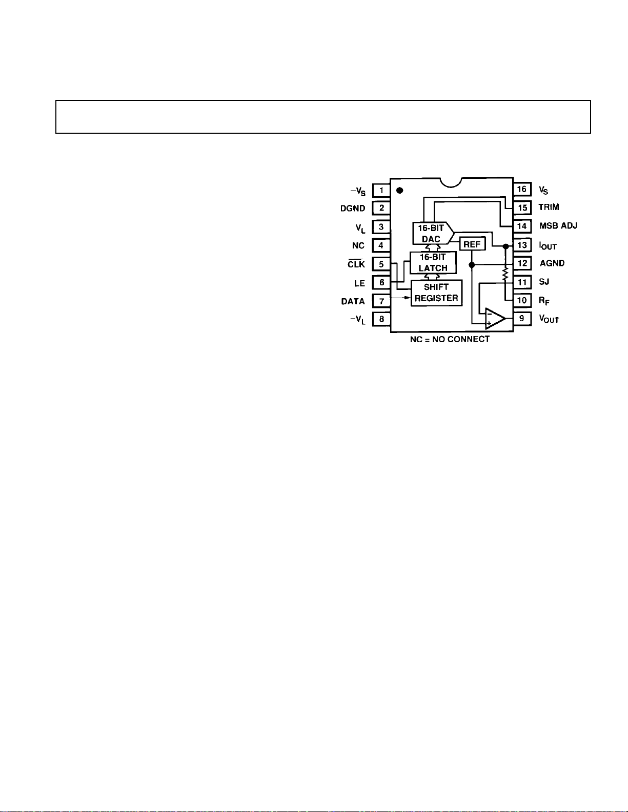
The AD766 16-bit DSP DACPORT provides a direct, threewire interface to the serial ports of popular DSP processors, including the ADSP-2101, TMS320CXX, and DSP56001. No
additional “glue logic” is required. The AD766 is also complete, offering on-chip serial-to-parallel input format conversion, a 16-bit current-steering DAC, voltage reference, and a
voltage output op amp. The AD766 is fabricated in Analog
Devices’ BiMOS II mixed-signal process which provides bipolar
transistors, MOS transistors, and thin-film resistors for precision analog circuits in addition to CMOS devices for logic.
The design and layout of the AD766 have been optimized for ac
performance and are responsible for its guaranteed and tested
94 dB signal-to-noise ratio to 20 kHz and 79 dB SNR to
250 kHz. Laser-trimming the AD766’s silicon chromium thinfilm resistors reduces total harmonic distortion below –81 dB
(at 1 kHz), a specification also production tested. An optional
linearity trim pin allows elimination of midscale differential
linearity error for even lower THD with small signals.
The AD766’s output amplifier provides a ±3 V signal with a
high slew rate, small glitch, and fast settling. The output amplifier is short circuit protected and can withstand indefinite shorts
to ground.
DSP DACPORT
AD766
FUNCTIONAL BLOCK DIAGRAM
The serial interface consists of bit clock, data, and latch enable
inputs. The twos-complement data word is clocked MSB first
on falling clock edges into the serial-to-parallel converter, consistent with the serial protocols of popular DSP processors. The
input clock can support data transfers up to 12.5 MHz. The
falling edge of latch enable updates the internal DAC input register at the sample rate with the sixteen bits most recently
clocked into the serial input register.
The AD766 operates over a ±5 V to ±12 V power supply range.
The digital supplies, +V
analog signal supplies, +V
crosstalk. Separate analog and digital ground pins are also provided. An internal bandgap reference provides a precision voltage source to the output amp that is stable over temperature and
time.
Power dissipation is typically 120 mW with ± 5 V supplies and
300 mW with ±12 V. The AD766 is available in commercial
(0°C to +70°C), industrial (–40°C to +85°C), and military
(–55°C to +125°C) grades. Commercial and industrial grade
parts are available in a 16-pin plastic DIP; military parts processed to MIL-STD-883B are packaged in a 16-pin ceramic
DIP. See Analog Devices’ Military Products Databook or current
military data sheet for specifications for the military version.
and –VL, can be separated from the
L
and –VS, for reduced digital
S
DACPORT is a registered trademark of Analog Devices, Inc.
REV. A
Information furnished by Analog Devices is believed to be accurate and
reliable. However, no responsibility is assumed by Analog Devices for its
use, nor for any infringements of patents or other rights of third parties
which may result from its use. No license is granted by implication or
otherwise under any patent or patent rights of Analog Devices.
One Technology Way, P.O. Box 9106, Norwood, MA 02062-9106, U.S.A.
Tel: 617/329-4700 Fax: 617/326-8703

AD766–SPECIFICATIONS
(T
to T
MIN
, 65 V supplies, FS = 500 kSPS unless otherwise noted. No deglitchers or
MAX
MSB trimming is used.)
Parameter Min Typ Max Min Typ Max Units
AD766J AD766A
RESOLUTION 16 16 Bits
DIGITAL INPUTS
V
IH
V
IL
IIH, VIH = V
L
2.0 +V
0.8 0.8 V
1.0 1.0 µA
L
2.0 +V
L
V
IIL, VIL = 0.4 –10 –10 µA
SERIAL PORT TIMING
Serial Clock Period (t
) 95 115 ns
CLK
Serial Clock HI (tHI)3030ns
Serial Clock LO (tLO)3070ns
Data Valid (t
)4040ns
DATA
Data Setup (tS)1520ns
Data Hold (tH)1520ns
Clock-to-Latch-Enable (t
Latch-Enable-to-Clock (t
Latch Enable HI (t
LEHI
Latch Enable LO (t
ACCURACY
1
LELO
) 80 100 ns
CTLE
)15 15 ns
LETC
)4040ns
)40 80ns
Gain Error ±2.0 ±2.0 % of FSR
Gain Drift ±25 ± 25 ppm of FSR/°C
Midscale Output Voltage Error ±30 ±30 mV
Bipolar Zero Drift ±4 ±4 ppm of FSR/°C
Differential Linearity Error ± 0.001 ±0.001 % of FSR
Monotonicity 15 15 Bits
TOTAL HARMONIC DISTORTION
F
= 1037 Hz
OU T
1
0 dB –88 –81 –88 –81 dB
–20 dB –75 –65 –75 –65 dB
–60 dB –37 –27 –37 –27 dB
F
= 49.07 kHz
OUT
2
0 dB –77 –72 –77 –72 dB
–20 dB –69 –66 –69 –66 dB
–60 dB –25 –21 –25 –21 dB
SIGNAL-TO-NOISE RATIO
20 Hz to 20 kHz (F
20 kHz to 250 kHz (F
SETTLING TIME (to ±0.0015% of FSR)
Voltage Output
1
= 1037 Hz)
OUT
= 49.07 kHz)
OUT
3
1
2
94 102 94 102 dB
79 83 79 83 dB
6 V Step 1.5 1.5 µs
1 LSB Step 1.0 1.0 µs
Slew Rate 9 9 V/µs
Current Output
1 mA Step 10 Ω to 100 Ω Load 350 350 ns
1 kΩ Load 350 350 ns
OUTPUT
Voltage Output Configuration
1
Bipolar Range ± 2.88 ± 3.0 ± 3.12 ± 2.88 ± 3.0 ± 3.12 V
Output Current ± 8.0 ±8.0 mA
Output Impedance 0.1 0.1 Ω
Short Circuit Duration Indefinite to Common Indefinite to Common
Current Output Configuration
Bipolar Range ± 0.7 ±1.0 ± 1.3 ±0.7 ± 1.0 ±1.3 mA
Output Impedance (± 30%) 1.7 1.7 kΩ
POWER SUPPLY
Voltage: +VL and +V
Voltage: –VL and –V
S
S
4.75 13.2 4.75 13.2 V
–13.2 –4.75 –13.2 –4.75 V
Current Case 11: VS and VL = +5 V +I 12.0 15.0 12.0 15.0 mA
Current Case 11: –VS and –VL = –5 V –I –12.0 –15.0 –12.0 –15.0 mA
Current Case 2:1 VS and VL = +12 V +I 10.5 10.5 mA
Current Case 2:1 –VS and –VL = –12 V –I –14 –14 mA
Current Case 34: VS and VL = +5 V +I 12 12 mA
Current Case 2:1 –VS and –VL = –12 V –I –14 –14 mA
Power Dissipation: VS and VL = ± 5 V
1
120 150 120 150 mW
Power Dissipation: VS and VL = ± 12 V 300 300 mW
Power Dissipation: VS and VL = +5 V,
Power Dissipation: –VS and –VL = –12 V
4
225 225 mW
–2–
REV. A

AD766
Parameter Min Typ Max Min Typ Max Units
TEMPERATURE RANGE
Specified 0 +70 –40 +85 °C
Storage –60 +100 –60 +100 °C
NOTES
1
For A grade only, voltage outputs are guaranteed only if +VS ≥ 7 V and –VS ≤ –7 V.
2
Specified using external op amp, see Figure 3 for more details.
3
Tested at full-scale input.
4
For A grade only, power supplies must be symmetric, i.e., VS = |–VS| and +VL = |–VL|. Each supply must independently meet this equality within ±5%.
All min and max specifications are guaranteed. Specifications in boldface are tested on all production units at final electrical test. Results from those tests are used to
calculate outgoing quality levels.
Specifications subject to change without notice.
ABSOLUTE MAXIMUM RATINGS*
VL to DGND . . . . . . . . . . . . . . . . . . . . . . . . . . . . . .0 to 13.2 V
V
to AGND . . . . . . . . . . . . . . . . . . . . . . . . . . . . . .0 to 13.2 V
S
–V
to DGND . . . . . . . . . . . . . . . . . . . . . . . . . . –13.2 V to 0 V
L
–V
to AGND . . . . . . . . . . . . . . . . . . . . . . . . . . –13.2 V to 0 V
S
Digital Inputs to DGND . . . . . . . . . . . . . . . . . . . .–0.3 V to V
AGND to DGND . . . . . . . . . . . . . . . . . . . . . . . . . . . . . ±0.3 V
Short Circuit Protection . . . . . . . . Indefinite Short to Ground
Soldering . . . . . . . . . . . . . . . . . . . . . . . . . . . . . +300°C, 10 sec
*Stresses greater than those listed under “Absolute Maximum Ratings” may cause
permanent damage to the device. This is a stress rating only and functional
operation of the device at these or any other conditions above those indicated in
the operational section of this specification is not implied. Exposure to absolute
maximum rating conditions for extended periods may affect device reliability.
AD766J AD766A
ORDERING GUIDE
Temperature Package
Model Range Option*
L
AD766JN 0°C to +70°C N-16
AD766AN –40°C to +85°C N-16
AD766SD/883B –55°C to +125°C D-16
*N = Plastic DIP; D = Ceramic DIP.
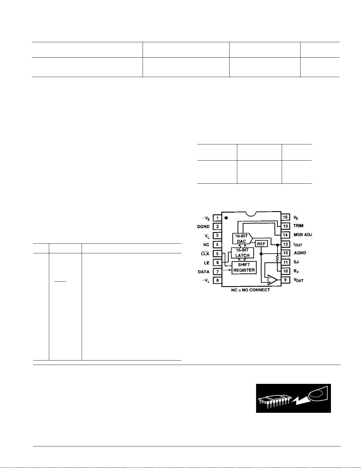
CONNECTION DIAGRAM
PIN DESIGNATIONS
Pin Function Description
1–V
S
Analog Negative Power Supply
2 DGND Digital Ground
3V
L
Logic Positive Power Supply
4 NC No Connection
5
CLK Clock Input
6 LE Latch Enable Input
7 DATA Serial Data Input
8–V
9V
10 R
L
OUT
F
Logic Negative Power Supply
Voltage Output
Feedback Resistor
11 SJ Summing Junction
12 AGND Analog Ground
13 I
OUT
Current Output
14 MSB ADJ MSB Adjustment Terminal
15 TRIM MSB Trimming Potentiometer Terminal
16 V
S
Analog Positive Power Supply
ESD SENSITIVITY
The AD766 features input protection circuitry consisting of large “distributed” diodes and
polysilicon series resistors to dissipate both high energy discharges (Human Body Model) and
fast, low energy pulses (Charged Device Model). Per Method 3015.2 of MIL-STD-883C, the
AD766 has been classified as a Category 1 Device.
Proper ESD precautions are strongly recommended to avoid functional damage or performance degradation. Charges as high as 4000 volts readily accumulate on the human body and
test equipment, and discharge without detection. Unused devices must be stored in conductive foam or shunts, and the foam discharged to the destination socket before devices are
removed. For further information on ESD precaution, refer to Analog Devices’ ESD
Prevention Manual.
WARNING!
ESD SENSITIVE DEVICE
REV. A
–3–
 Loading...