ANALOG DEVICES AD7656-1, AD7657-1, AD7658-1 Service Manual
现货库存、技术资料、百科信息、热点资讯,精彩尽在鼎好!
V
A
A
250 kSPS, 6-Channel, Simultaneous
Sampling, Bipolar, 16-/14-/12-Bit ADC
FEATURES
Pin and software compatible with AD7656/AD7657/AD7658
featuring reduced decoupling requirements
6 independent ADCs
True bipolar analog inputs
Pin-/software-selectable ranges: ±10 V, ±5 V
Fast throughput rate: 250 kSPS
iCMOS process technology
Low power
140 mW at 250 kSPS with 5 V supplies
High noise performance with wide bandwidth
88 dB SNR at 10 kHz input frequency
On-chip reference and reference buffers
High speed parallel, serial, and daisy-chain interface modes
High speed serial interface
SPI/QSPI™/MICROWIRE™/DSP compatible
Standby mode: 25 μW max
64-lead LQFP
APPLICATIONS
Power line monitoring and measuring systems
Instrumentation and control systems
Multiaxis positioning systems
AD7656-1/AD7657-1/AD7658-1
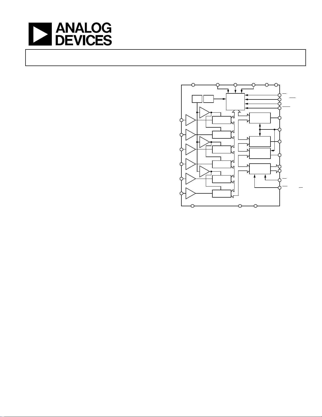
FUNCTIONAL BLOCK DIAGRAM
BUF
BUF
BUF
CONVST
CLK
OSC
DD
REF
T/H
V1
V2
T/H
T/H
V3
T/H
V4
T/H
V5
T/H
V6
V
SS
CONVST B CONVST C
CONTROL
LOGIC
16-/14-/
12-BIT SAR
16-/14-/
12-BIT SAR
16-/14-/
12-BIT SAR
16-/14-/
12-BIT SAR
16-/14-/
12-BIT SAR
16-/14-/
12-BIT SAR
AD7656-1/AD7657-1/AD7658-1
AGND
OUTPUT
DRIVERS
OUTPUT
DRIVERS
OUTPUT
DRIVERS
OUTPUT
DRIVERS
DGND
Figure 1.
VCCDV
CC
CS
SER/PAR SEL
V
DRIVE
STBY
DB8/DOUT A
DB6/SCLK
DB9/DOUT B
DB10/DOUT C
DATA/
CONTROL
LINES
RD
WR/REF
07017-001
EN/DIS
GENERAL DESCRIPTION
The AD7656-1/AD7657-1/AD7658-11 are reduced decoupling pinand software-compatible versions of AD7656/AD7657/AD7658.
The AD7656-1/AD7657-1/AD7658-1 devices contain six 16-/
14-/12-bit, fast, low power successive approximation ADCs in
a package designed on the iCMOS® process (industrial CMOS).
iCMOS is a process combining high voltage silicon with submicron
CMOS and complementary bipolar technologies. It enables the
development of a wide range of high performance analog ICs
capable of 33 V operation in a footprint that no previous generation
of high voltage parts could achieve. Unlike analog ICs using conventional CMOS processes, iCMOS components can accept bipolar
input signals while providing increased performance, which
dramatically reduces power consumption and package size.
The AD7656-1/AD7657-1/AD7658-1 feature throughput rates
of up to 250 kSPS. The parts contain low noise, wide bandwidth
track-and-hold amplifiers that can handle input frequencies
up to 4.5 MHz.
1
Protected by U.S. Patent No. 6,731,232.
Rev. 0
Information furnished by Analog Devices is believed to be accurate and reliable. However, no
responsibility is assumed by Analog Devices for its use, nor for any infringements of patents or other
rights of third parties that may result from its use. Specifications subject to change without notice. No
license is granted by implication or otherwise under any patent or patent rights of Analog Devices.
Trademarks and registered trademarks are the property of their respective owners.
The conversion process and data acquisition are controlled
using the CONVST signals and an internal oscillator. Three
CONVST pins (CONVST A, CONVST B, and CONVST C)
allow independent, simultaneous sampling of the three ADC
pairs. The AD7656-1/AD7657-1/AD7658-1 have a high speed
parallel and serial interface, allowing the devices to interface with
microprocessors or DSPs. When the serial interface is selected,
each part has a daisy-chain feature that allows multiple ADCs to
connect to a single serial interface. The AD7656-1/AD7657-1/
AD7658-1 can accommodate true bipolar input signals in the
±4 × V
and ±2 × V
REF
ranges. Each AD7656-1/AD7657-1/
REF
AD7658-1 also contains an on-chip 2.5 V reference.
PRODUCT HIGHLIGHTS
1. Six 16-/14-/12-bit, 250 kSPS ADCs on board.
2. Six true bipolar, high impedance analog inputs.
3. High speed parallel and serial interfaces.
4. Reduced decoupling requirements and reduced bill of
materials cost compared with the AD7656/AD7657/
AD7658 devices.
One Technology Way, P.O. Box 9106, Norwood, MA 02062-9106, U.S.A.
Tel: 781.329.4700 www.analog.com
Fax: 781.461.3113 ©2008 Analog Devices, Inc. All rights reserved.

AD7656-1/AD7657-1/AD7658-1
TABLE OF CONTENTS
Features .............................................................................................. 1
Applications ....................................................................................... 1
Functional Block Diagram .............................................................. 1
General Description ......................................................................... 1
Product Highlights ........................................................................... 1
Revision History ............................................................................... 2
Specifications ..................................................................................... 3
AD7656-1 ...................................................................................... 3
AD7657-1 ...................................................................................... 5
AD7658-1 ...................................................................................... 7
Timing Specifications .................................................................. 9
Absolute Maximum Ratings .......................................................... 10
Thermal Resistance .................................................................... 10
ESD Caution ................................................................................ 10
Pin Configuration and Function Descriptions ........................... 11
Typical Performance Characteristics ........................................... 14
Terminology .................................................................................... 18
Theory of Operation ...................................................................... 20
Converter Details ....................................................................... 20
ADC Transfer Function ............................................................. 21
Internal/External Reference ...................................................... 21
Typical Connection Diagram ................................................... 21
Driving the Analog Inputs ........................................................ 22
Interface Options ........................................................................ 22
Application Hints ........................................................................... 29
Layout .......................................................................................... 29
Outline Dimensions ....................................................................... 30
Ordering Guide .......................................................................... 30
REVISION HISTORY
7/08—Revision 0: Initial Version
Rev. 0 | Page 2 of 32

AD7656-1/AD7657-1/AD7658-1
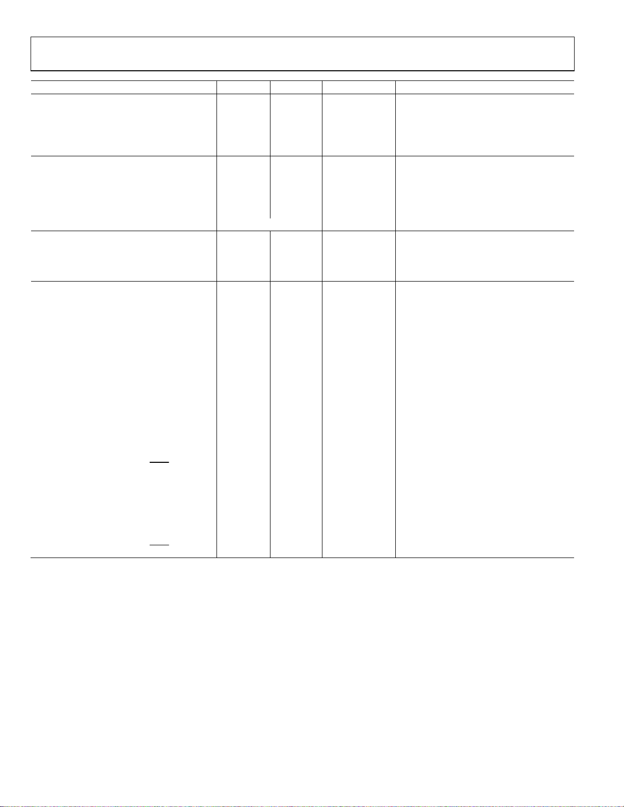
SPECIFICATIONS
AD7656-1
V
= 2.5 V internal/external, AVCC = 4.75 V to 5.25 V, DVCC = 4.75 V to 5.25 V, V
REF
10 V to 16.5 V, V
T
, unless otherwise noted.
MAX
= −10 V to −16.5 V; for the ±2 × V
SS
range, VDD = 5 V to 16.5 V, VSS = −5 V to −16.5 V; f
REF
Table 1.
Parameter B Version1Y Version1Unit Test Conditions/Comments
DYNAMIC PERFORMANCE fIN = 10 kHz sine wave
Signal-to-(Noise + Distortion) (SINAD)2 88 88 dB typ
Signal-to-Noise Ratio (SNR)2 88 88 dB typ
Total Harmonic Distortion (THD)
2
−90 −90 dB max
−105 −105 dB typ VDD/VSS = ±5 V to ±16.5 V
Peak Harmonic or Spurious Noise (SFDR)2 −100 −100 dB typ
Intermodulation Distortion (IMD)2 fa = 10.5 kHz, fb = 9.5 kHz
Second-Order Terms −112 −112 dB typ
Third-Order Terms −107 −107 dB typ
Aperture Delay 10 10 ns max
Aperture Delay Matching 4 4 ns max
Aperture Jitter 35 35 ps typ
Channel-to-Channel Isolation
2
−100 −100 dB typ f
Full-Power Bandwidth 4.5 4.5 MHz typ @ −3 dB
2.2 2.2 MHz typ @ −0.1 dB
DC ACCURACY
Resolution 16 16 Bits
No Missing Codes 15 14 Bits min
Integral Nonlinearity
2
±3 ±3 LSB max
±1 ±1 LSB typ
Positive Full-Scale Error
Positive Full-Scale Error Matching
2
±0.8 ±0.8 % FS max ±0.381% FSR typical
2
±0.35 ±0.35 % FS max
Bipolar Zero-Scale Error2 ±0.048 ±0.023 % FS max ±0.0137% FSR typical
Bipolar Zero-Scale Error Matching
Negative Full-Scale Error
2
±0.8 ±0.8 % FS max ±0.381% FSR typical
Negative Full-Scale Error Matching
2
±0.038 ±0.038 % FS max
2
±0.35 ±0.35 % FS max
ANALOG INPUT
Input Voltage Ranges ±4 × V
±2 × V
±4 × V
REF
±2 × V
REF
V RNGx bits or RANGE pin = 0
REF
V RNGx bits or RANGE pin = 1
REF
DC Leakage Current ±1 ±1 μA max
Input Capacitance
3
10 10 pF typ ±4 × V
14 14 pF typ ±2 × V
REFERENCE INPUT/OUTPUT
Reference Input Voltage Range 2.5 2.5 V min/max
DC Leakage Current ±1 ±1 μA max
Input Capacitance
3
18.5 18.5 pF typ
Reference Output Voltage 2.49/2.51 2.49/2.51 V min/max
Long-Term Stability 150 150 ppm typ 1000 hours
Reference Temperature Coefficient 25 25 ppm/°C max
6 6 ppm/°C typ
= 2.7 V to 5.25 V; for the ±4 × V
DRIVE
SAMPLE
on unselected channels up to 100 kHz
IN
See Tab le 8 for minimum V
each range
range when in track
REF
range when in track
REF
= 1
REF
DIS
EN/
range, VDD =
REF
= 250 kSPS, TA = T
for
DD/VSS
MIN
to
Rev. 0 | Page 3 of 32
AD7656-1/AD7657-1/AD7658-1
Parameter B Version1Y Version
1
Unit Test Conditions/Comments
LOGIC INPUTS
Input High Voltage (V
Input Low Voltage (V
) 0.7 × V
INH
) 0.3 × V
INL
0.7 × V
DRIVE
0.3 × V
DRIVE
V min
DRIVE
V max
DRIVE
Input Current (IIN) ±10 ±10 μA max Typically 10 nA, VIN = 0 V or V
Input Capacitance (CIN)3 10 10 pF max
LOGIC OUTPUTS
Output High Voltage (VOH) V
Output Low Voltage (VOL) 0.2 0.2 V max I
− 0.2 V
DRIVE
− 0.2 V min I
DRIVE
= 200 μA
SOURCE
= 200 μA
SINK
Floating-State Leakage Current ±10 ±10 μA max
Floating-State Output Capacitance
3
10 10 pF max
Output Coding Twos complement
CONVERSION RATE
Conversion Time 3.1 3.1 μs max
Track-and-Hold Acquisition Time
2, 3
550 550 ns max
Throughput Rate 250 250 kSPS Parallel interface mode only
POWER REQUIREMENTS
VDD 5/15 5/15 V nom min/max For the 4 × V
VSS −5/−15 −5/−15 V nom min/max For the 4 × V
range, VDD = 10 V to 16.5 V
REF
range, VDD = −10 V to −16.5 V
REF
AVCC 5 5 V nom
DVCC 5 5 V nom
V
3/5 3/5 V nom min/max
DRIVE
4
I
TOTAL
Normal Mode—Static 18 18 mA max
Normal Mode—Operational 26 26 mA max
ISS (Operational) 0.25 0.25 mA max VSS = −16.5 V, f
I
(Operational) 0.25 0.25 mA max VDD = 16.5 V, f
DD
Partial Power-Down Mode 7 7 mA max
Full Power-Down Mode (STBY Pin)
Power Dissipation
Digital inputs = 0 V or V
400 400 μA max
= DVCC = V
AV
CC
V
= −16.5 V
SS
= 250 kSPS, AVCC = DVCC = V
f
SAMPLE
= 16.5 V, VSS = −16.5 V
V
DD
= DVCC = V
AV
CC
= −16.5 V
V
SS
SCLK on or off, AVCC = DVCC = V
V
= 16.5 V, VSS = −16.5 V
DD
= DV
AV
CC
CC
= −16.5 V
V
SS
= 5.25 V, VDD = 16.5 V,
DRIVE
= 250 kSPS
SAMPLE
= 250 kSPS
SAMPLE
= 5.25 V, VDD = 16.5 V,
DRIVE
= V
= 5.25 V, VDD = 16.5 V,
DRIVE
Normal Mode—Static 94 94 mW max
Normal Mode—Operational 140 140 mW max f
= 250 kSPS
SAMPLE
Partial Power-Down Mode 40 40 mW max
Full Power-Down Mode (STBY Pin)
1
The temperature range for the B version is −40°C to +85°C and for the Y version is −40°C to +125°C.
2
See the Terminology section.
3
Sample tested during initial release to ensure compliance.
4
Includes I
AVCC
, I
, I
, I
, and I
VDD
VSS
VDRIVE
DVCC
.
25 25 μW max
DRIVE
DRIVE
DRIVE
= 5.25 V,
DRIVE
= 5.25 V,
Rev. 0 | Page 4 of 32

AD7656-1/AD7657-1/AD7658-1
AD7657-1
V
= 2.5 V internal/external, AVCC = 4.75 V to 5.25 V, DVCC = 4.75 V to 5.25 V, V
REF
10 V to 16.5 V, V
T
, unless otherwise noted.
MAX
= −10 V to −16.5 V; for the ±2 × V
SS
range, VDD = 5 V to 16.5 V, VSS = −5 V to −16.5 V; f
REF
Table 2.
Parameter B Version1Y Version1Unit Test Conditions/Comments
DYNAMIC PERFORMANCE fIN = 10 kHz sine wave
Signal-to-(Noise + Distortion) (SINAD)2 82.5 82.5 dB typ
Signal-to-Noise Ratio (SNR)
Total Harmonic Distortion (THD)
2
83.5 83.5 dB typ
2
−90 −90 dB max
−105 −105 dB typ
Peak Harmonic or Spurious Noise (SFDR)
2
−100 −100 dB typ
Intermodulation Distortion (IMD)2 fa = 10.5 kHz, fb = 9.5 kHz
Second-Order Terms −109 −109 dB typ
Third-Order Terms −104 −104 dB typ
Aperture Delay 10 10 ns max
Aperture Delay Matching 4 4 ns max
Aperture Jitter 35 35 ps typ
Channel-to-Channel Isolation
2
−100 −100 dB typ f
Full-Power Bandwidth 4.5 4.5 MHz typ @ −3 dB
2.2 2.2 MHz typ @ −0.1 dB
DC ACCURACY
Resolution 14 14 Bits
No Missing Codes 14 14 Bits min
Integral Nonlinearity
2
±1 ±1 LSB max
±1 ±1 LSB typ
Positive Full-Scale Error
Positive Full-Scale Error Matching
2
±0.95 ±0.95 % FS max ±0.27% FSR typical
2
±0.366 ±0.366 % FS max
Bipolar Zero-Scale Error2 ±0.04 ±0.04 % FS max ±0.016% FSR typical
Bipolar Zero-Scale Error Matching
Negative Full-Scale Error
2
±0.95 ±0.95 % FS max ±0.27% FSR typical
Negative Full-Scale Error Matching
2
±0.0427 ±0.0427 % FS max
2
±0.366 ±0.366 % FS max
ANALOG INPUT
Input Voltage Ranges ±4 × V
±2 × V
±4 × V
REF
±2 × V
REF
V RNGx bits or RANGE pin = 0
REF
V RNGx bits or RANGE pin = 1
REF
DC Leakage Current ±1 ±1 μA max
Input Capacitance
3
10 10 pF typ ±4 × V
14 14 pF typ ±2 × V
REFERENCE INPUT/OUTPUT
Reference Input Voltage Range 2.5 2.5 V min/max
DC Leakage Current ±1 ±1 μA max
Input Capacitance
3
18.5 18.5 pF typ
Reference Output Voltage 2.49/2.51 2.49/2.51 V min/max
Long-Term Stability 150 150 ppm typ 1000 hours
Reference Temperature Coefficient 25 25 ppm/°C max
6 6 ppm/°C typ
LOGIC INPUTS
Input High Voltage (V
Input Low Voltage (V
) 0.7 × V
INH
) 0.3 × V
INL
0.7 × V
DRIVE
0.3 × V
DRIVE
V min
DRIVE
V max
DRIVE
Input Current (IIN) ±10 ±10 μA max Typically 10 nA, VIN = 0 V or V
Input Capacitance (CIN)3 10 10 pF max
= 2.7 V to 5.25 V; for the ±4 × V
DRIVE
SAMPLE
on unselected channels up to 100 kHz
IN
See Tab le 8 for minimum V
each range
range when in track
REF
range when in track
REF
REF
= 1
DIS
EN/
range, VDD =
REF
= 250 kSPS, TA = T
for
DD/VSS
DRIVE
MIN
to
Rev. 0 | Page 5 of 32

AD7656-1/AD7657-1/AD7658-1
Parameter B Version1Y Version
1
Unit Test Conditions/Comments
LOGIC OUTPUTS
Output High Voltage (VOH) V
Output Low Voltage (VOL) 0.2 0.2 V max I
− 0.2 V
DRIVE
− 0.2 V min I
DRIVE
= 200 μA
SOURCE
= 200 μA
SINK
Floating-State Leakage Current ±10 ±10 μA max
Floating-State Output Capacitance
3
10 10 pF max
Output Coding Twos complement
CONVERSION RATE
Conversion Time 3.1 3.1 μs max
Track-and-Hold Acquisition Time
2, 3
550 550 ns max
Throughput Rate 250 250 kSPS Parallel interface mode only
POWER REQUIREMENTS
VDD 5/15 5/15 V nom min/max For the 4 × V
VSS −5/−15 −5/−15 V nom min/max For the 4 × V
range, VDD = 10 V to 16.5 V
REF
range, VDD = −10 V to −16.5 V
REF
AVCC 5 5 V nom
DVCC 5 5 V nom
V
3/5 3/5 V nom min/max
DRIVE
4
I
TOTAL
Normal Mode—Static 18 18 mA max
Normal Mode—Operational 26 26 mA max
ISS (Operational) 0.25 0.25 mA max VSS = −16.5 V, f
I
(Operational) 0.25 0.25 mA max VDD = 16.5 V, f
DD
Partial Power-Down Mode 7 7 mA max
Full Power-Down Mode (STBY Pin)
Power Dissipation
Digital inputs = 0 V or V
400 400 μA max
= DVCC = V
AV
CC
V
= −16.5 V
SS
= 250 kSPS, AVCC = DVCC = V
f
SAMPLE
= 16.5 V, VSS = −16.5 V
V
DD
= DVCC = V
AV
CC
V
= −16.5 V
SS
SCLK on or off, AVCC = DVCC = V
= 16.5 V, VSS = −16.5 V
V
DD
= DV
AV
CC
CC
= −16.5 V
V
SS
= 5.25 V, VDD = 16.5 V,
DRIVE
= 250 kSPS
SAMPLE
= 250 kSPS
SAMPLE
= 5.25 V, VDD = 16.5 V,
DRIVE
= V
= 5.25 V, VDD = 16.5 V,
DRIVE
Normal Mode—Static 94 94 mW max
Normal Mode—Operational 140 140 mW max f
= 250 kSPS
SAMPLE
Partial Power-Down Mode 40 40 mW max
Full Power-Down Mode (STBY Pin)
1
The temperature range for the B version is −40°C to +85°C and for the Y version is −40°C to +125°C.
2
See the Terminology section.
3
Sample tested during initial release to ensure compliance.
4
Includes I
AVCC
, I
, I
, I
, and I
VDD
VSS
VDRIVE
DVCC
.
25 25 μW max
DRIVE
DRIVE
= 5.25 V,
DRIVE
= 5.25 V,
Rev. 0 | Page 6 of 32

AD7656-1/AD7657-1/AD7658-1
AD7658-1
V
= 2.5 V internal/external, AVCC = 4.75 V to 5.25 V, DVCC = 4.75 V to 5.25 V, V
REF
to 16.5 V, V
= −10 V to −16.5 V; for ±2 × V
SS
range, VDD = 5 V to 16.5 V, VSS = −5 V to −16.5 V; f
REF
unless otherwise noted.
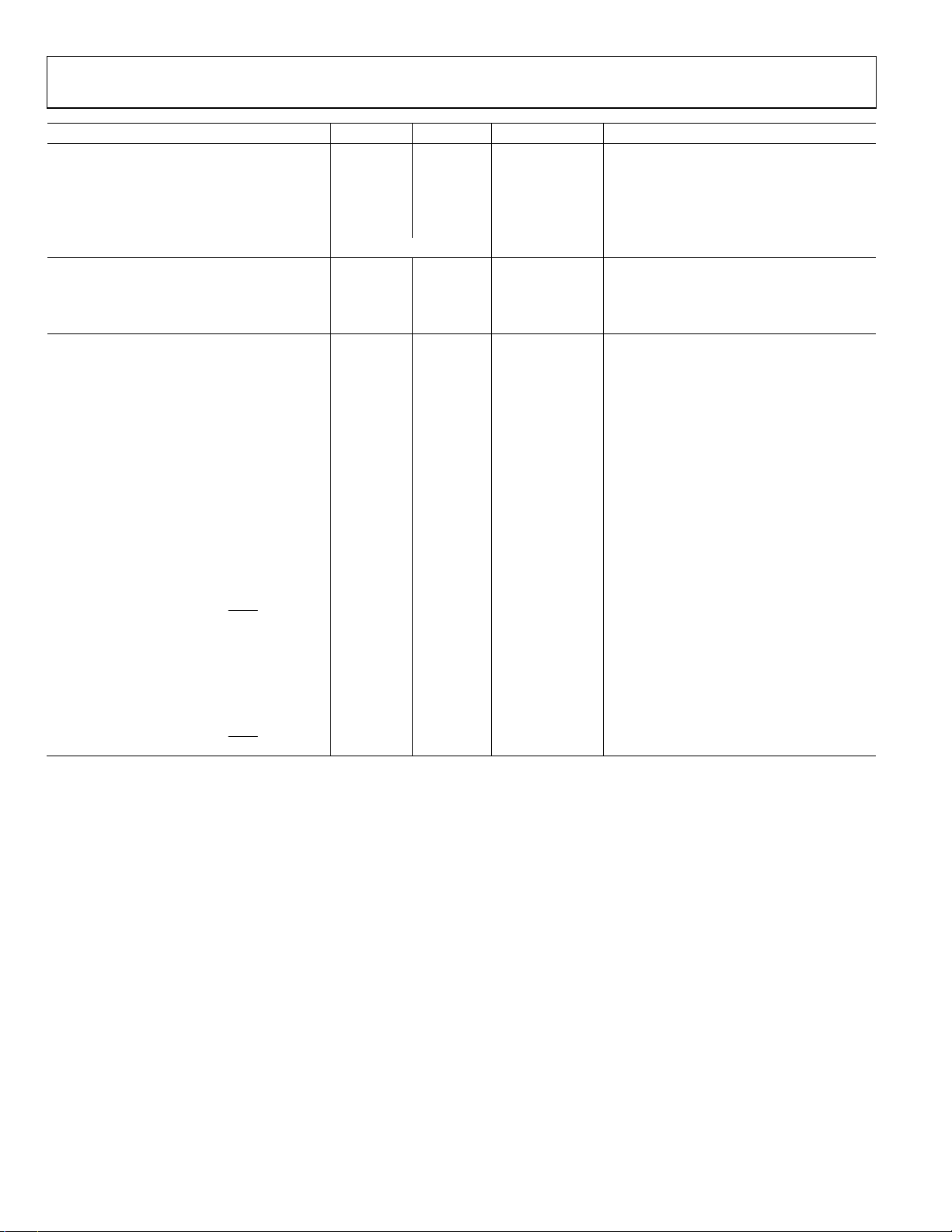
Table 3.
Parameter B Version1Y Version1Unit Test Conditions/Comments
DYNAMIC PERFORMANCE fIN = 10 kHz sine wave
Signal-to-(Noise + Distortion) (SINAD)2 73.5 73.5 dB typ
73.5 73.5 dB typ
Total Harmonic Distortion (THD)
2
−88 −88 dB max
−100 −100 dB typ
Peak Harmonic or Spurious Noise (SFDR)
2
−97 −97 dB typ
Intermodulation Distortion (IMD)2 fa = 10.5 kHz, fb = 9.5 kHz
Second-Order Terms −106 −106 dB typ
Third-Order Terms −101 −101 dB typ
Aperture Delay 10 10 ns max
Aperture Delay Matching 4 4 ns max
Aperture Jitter 35 35 ps typ
Channel-to-Channel Isolation
2
−100 −100 dB typ f
Full-Power Bandwidth 4.5 4.5 MHz typ @ −3 dB
2.2 2.2 MHz typ @ −0.1 dB
DC ACCURACY
Resolution 12 12 Bits
No Missing Codes 12 12 Bits min
Differential Nonlinearity ±0.7 ±0.7 LSB max
Integral Nonlinearity
Positive Full-Scale Error
Positive Full-Scale Error Matching
2
±0.5 ±0.5 LSB max
2
±0.95 ±0.95 % FS max ±0.317% FSR typical
2
±0.366 ±0.366 % FS max
Bipolar Zero-Scale Error2 ±2 ±2 LSB max ±0.0125% FSR typical
Bipolar Zero-Scale Error Matching
Negative Full-Scale Error
2
±0.95 ±0.95 % FS max ±0.317% FSR typical
Negative Full-Scale Error Matching
2
±2 ±2 LSB max
2
±0.366 ±0.366 % FS max
ANALOG INPUT
Input Voltage Ranges ±4 × V
±2 × V
±4 × V
REF
±2 × V
REF
V RNGx bits or RANGE pin = 0
REF
V RNGx bits or RANGE pin = 1
REF
DC Leakage Current ±1 ±1 μA max
Input Capacitance
3
10 10 pF typ ±4 × V
14 14 pF typ ±2 × V
REFERENCE INPUT/OUTPUT
Reference Input Voltage Range 2.5 2.5 V min/max
DC Leakage Current ±1 ±1 μA max
Input Capacitance
3
18.5 18.5 pF typ
Reference Output Voltage 2.49/2.51 2.49/2.51 V min/max
Long-Term Stability 150 150 ppm typ 1000 hours
Reference Temperature Coefficient 25 25 ppm/°C max
6 6 ppm/°C typ
LOGIC INPUTS
Input High Voltage (V
Input Low Voltage (V
) 0.7 × V
INH
) 0.3 × V
INL
0.7 × V
DRIVE
0.3 × V
DRIVE
V min
DRIVE
V max
DRIVE
Input Current (IIN) ±10 ±10 μA max Typically 10 nA, VIN = 0 V or V
Input Capacitance (CIN)3 10 10 pF max
= 2.7 V to 5.25 V; for ±4 × V
DRIVE
= 250 kSPS, TA = T
SAMPLE
on unselected channels up to 100 kHz
IN
See Tab le 8 for minimum V
each range
range when in track
REF
range when in track
REF
REF
= 1
DIS
EN/
range, VDD = 10 V
REF
to T
MIN
for
DD/VSS
DRIVE
MAX
,
Rev. 0 | Page 7 of 32
AD7656-1/AD7657-1/AD7658-1
Parameter B Version1Y Version
1
Unit Test Conditions/Comments
LOGIC OUTPUTS
Output High Voltage (VOH) V
Output Low Voltage (VOL) 0.2 0.2 V max I
− 0.2 V
DRIVE
− 0.2 V min I
DRIVE
= 200 μA
SOURCE
= 200 μA
SINK
Floating-State Leakage Current ±10 ±10 μA max
Floating-State Output Capacitance
3
10 10 pF max
Output Coding Twos complement
CONVERSION RATE
Conversion Time 3.1 3.1 μs max
Track-and-Hold Acquisition Time
2, 3
550 550 ns max
Throughput Rate 250 250 kSPS Parallel interface mode only
POWER REQUIREMENTS
VDD 5/15 5/15 V nom min/max For the 4 × V
VSS −5/−15 −5/−15 V nom min/max For the 4 × V
range, VDD = 10 V to 16.5 V
REF
range, VDD = −10 V to −16.5 V
REF
AVCC 5 5 V nom
DVCC 5 5 V nom
V
3/5 3/5 V nom min/max
DRIVE
4
I
TOTAL
Normal Mode—Static 18 18 mA max
Normal Mode—Operational 26 26 mA max
ISS (Operational) 0.25 0.25 mA max VSS = −16.5 V, f
I
(Operational) 0.25 0.25 mA max VDD = 16.5 V, f
DD
Partial Power-Down Mode 7 7 mA max
Full Power-Down Mode (STBY Pin)
Power Dissipation
Digital inputs = 0 V or V
400 400 μA max
= DVCC = V
AV
CC
V
= −16.5 V
SS
= 250 kSPS, AVCC = DVCC = V
f
SAMPLE
= 16.5 V, VSS = −16.5 V
V
DD
= DVCC = V
AV
CC
V
= −16.5 V
SS
SCLK on or off, AVCC = DVCC = V
= 16.5 V, VSS = −16.5 V
V
DD
= DVCC = V
AV
CC
= −16.5 V
V
SS
= 5.25 V, VDD = 16.5 V,
DRIVE
= 250 kSPS
SAMPLE
= 250 kSPS
SAMPLE
= 5.25 V, VDD = 16.5 V,
DRIVE
= 5.25 V, VDD = 16.5 V,
DRIVE
Normal Mode—Static 94 94 mW max
Normal Mode—Operational 140 140 mW max f
= 250 kSPS
SAMPLE
Partial Power-Down Mode 40 40 mW max
Full Power-Down Mode (STBY Pin)
1
The temperature range for the B version is −40°C to +85°C and for the Y version is −40°C to +125°C
2
See the Terminology section.
3
Sample tested during initial release to ensure compliance.
4
Includes I
AVCC
, I
, I
, I
, and I
VDD
VSS
VDRIVE
DVCC
.
25 25 μW max
DRIVE
DRIVE
= 5.25 V,
DRIVE
= 5.25 V,
Rev. 0 | Page 8 of 32
AD7656-1/AD7657-1/AD7658-1
TIMING SPECIFICATIONS
AVCC/DVCC = 4.75 V to 5.25 V, VDD = 5 V to 16.5 V, VSS = −5 V to −16.5 V, V
T
= T
MIN
to T
A
, unless otherwise noted.
MAX
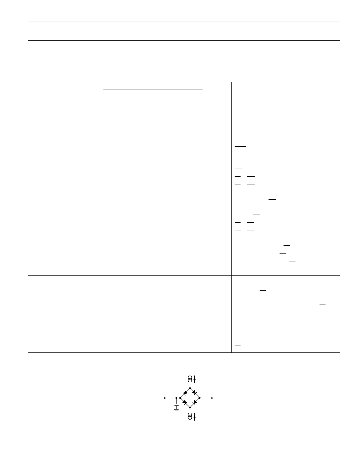
Table 4.
Parameter
1
V
< 4.75 V V
DRIVE
DRIVE
Limit at t
MIN, tMAX
= 4.75 V to 5.25 V
PARALLEL INTERFACE
t
3 3 μs typ Conversion time, internal clock
CONVER T
t
150 150 ns min
QUIET
t
550 550 ns min Acquisition time
ACQ
t10 25 25 ns min Minimum CONVST low pulse
t1 60 60 ns min CONVST high to BUSY high
t
2 2 ms max
WAKE -UP
25 25 μs max Partial power-down mode
PARALLEL WRITE OPERATION
t11 15 15 ns min
t12 0 0 ns min
t13 5 5 ns min
t14 5 5 ns min
t15 5 5 ns min
PARALLEL READ OPERATION
t
2
0 0 ns min
t3 0 0 ns min
t4 0 0 ns min
t5 45 36 ns min
t6 45 36 ns max
t7 10 10 ns min
t8 12 12 ns max
t9 6 6 ns min Minimum time between reads
SERIAL INTERFACE
f
18 18 MHz max Frequency of serial read clock
SCLK
t16 12 12 ns max
2
t
22 22 ns max
17
t18 0.4 × t
t19 0.4 × t
0.4 × t
SCLK
0.4 × t
SCLK
ns min SCLK low pulse width
SCLK
ns min SCLK high pulse width
SCLK
t20 10 10 ns min
t21 18 18 ns max
1
Sample tested during initial release to ensure compliance. All input signals are specified with tR = tF = 5 ns (10% to 90% of VDD) and timed from a voltage level of 1.6 V.
2
A buffer is used on the DOUTx pins (Pin 5 to Pin 7) for this measurement.
200µA I
= 2.7 V to 5.25 V, V
DRIVE
= 2.5 V internal/external,
REF
Unit Description
Minimum quiet time required between bus
relinquish and start of next conversion
rising edge to CONVST rising edge
STBY
pulse width
WR
to WR setup time
CS
to WR hold time
CS
Data setup time before WR
Data hold after WR
BUSY to RD
to RD setup time
CS
to RD hold time
CS
pulse width
RD
delay
Data access time after RD
Data hold time after RD
Bus relinquish time after RD
Delay from CS
disabled
Data access time after SCLK rising edge/CS
falling edge
SCLK to data valid hold time after SCLK
falling edge
rising edge to DOUTx high impedance
CS
OL
rising edge
rising edge
falling edge
rising edge
rising edge
until DOUTx three-state
TO OUTPUT
PIN
C
L
25pF
200µA I
Figure 2. Load Circuit for Digital Output Timing Specifications
Rev. 0 | Page 9 of 32
1.6V
OH
07017-002
AD7656-1/AD7657-1/AD7658-1
ABSOLUTE MAXIMUM RATINGS
TA = 25°C, unless otherwise noted.
Table 5.
Parameter Rating
VDD to AGND, DGND −0.3 V to +16.5 V
VSS to AGND, DGND +0.3 V to −16.5 V
VDD to AVCC V
− 0.3 V to 16.5 V
CC
AVCC to AGND, DGND −0.3 V to +7 V
DVCC to AVCC −0.3 V to AV
+ 0.3 V
CC
DVCC to DGND, AGND −0.3 V to +7 V
AGND to DGND −0.3 V to +0.3 V
V
to DGND −0.3 V to DVCC + 0.3 V
DRIVE
Analog Input Voltage to AGND1 V
Digital Input Voltage to DGND −0.3 V to V
Digital Output Voltage to DGND −0.3 V to V
− 0.3 V to VDD + 0.3 V
SS
+ 0.3 V
DRIVE
+ 0.3 V
DRIVE
REFIN/REFOUT to AGND −0.3 V to AVCC + 0.3 V
Input Current to Any Pin Except
Supplies
2
±10 mA
Operating Temperature Range
B Version −40°C to +85°C
Y Version −40°C to +125°C
Storage Temperature Range −65°C to +150°C
Junction Temperature 150°C
Pb/Sn Temperature, Soldering
Reflow (10 sec to 30 sec) 240(+0)°C
Pb-Free Temperature, Soldering Reflow 260(+0)°C
ESD 700 V
1
If the analog inputs are driven from alternative VDD and VSS supply circuitry,
a 240 Ω series resistor should be placed on the analog inputs and Schottky
diodes should be placed in series with the AD7656-1/AD7657-1/AD7658-1’s
VDD and VSS supplies.
2
Transient currents of up to 100 mA do not cause SCR latch-up.
Stresses above those listed under Absolute Maximum Ratings
may cause permanent damage to the device. This is a stress
rating only; functional operation of the device at these or any
other conditions above those indicated in the operational
section of this specification is not implied. Exposure to absolute
maximum rating conditions for extended periods may affect
device reliability.
THERMAL RESISTANCE
θJA is specified for the worst-case conditions, that is, a device
soldered in a circuit board for surface-mount packages. These
specifications apply to a 4-layer board.
Table 6. Thermal Resistance
Package Type θJA θ
Unit
JC
64-Lead LQFP 45 11 °C/W
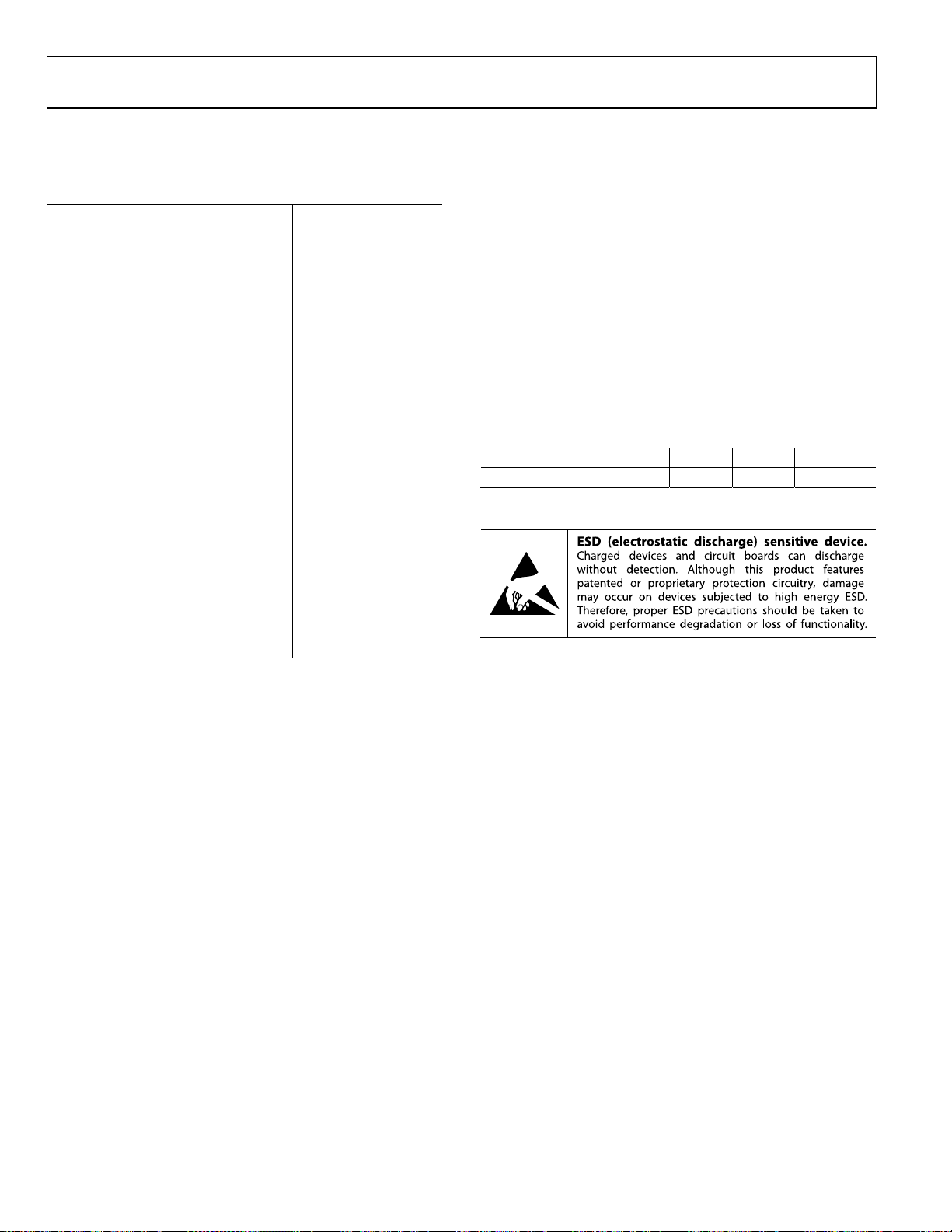
ESD CAUTION
Rev. 0 | Page 10 of 32
 Loading...