ANALOG DEVICES AD7658, AD7657, AD7656 Service Manual

现货库存、技术资料、百科信息、热点资讯,精彩尽在鼎好!
250 kSPS, 6-Channel,Simultaneous
Preliminary Technical Data
Sampling, Bipolar 12/14/16-Bit ADC
AD7658/AD7657/AD7656*
FEATURES
6 Independent ADCs
V
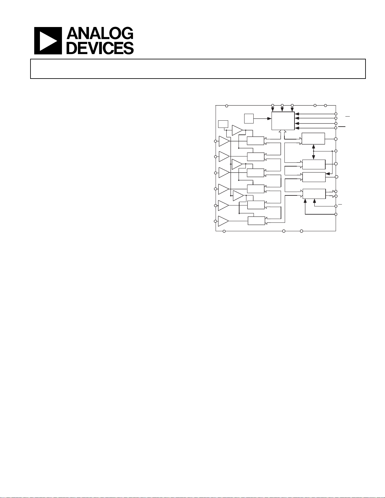
FUNCTIONAL BLOCK DIAGRAM
CONVSTB
DD
CONVSTA
CONVSTC
AV
DV
CC
CC
True Bipolar Analog Inputs
Pin/Software Selectable Ranges:- ±10V, ±5V
Fast throughput rate: 250 kSPS
Specified for V
of 4.5 V to 5.5 V
CC
Low power
160mW at 250 kSPS with 5 V supplies
Wide input bandwidth:
85 dB SNR at 50 kHz input frequency
On-chip Reference and Reference Buffers
Parallel and Serial Interface
High speed serial interface
SPI/QSPI/µWire/DSP compatible
Standby mode: 5 µA max
TM
iCMOS
Process Technology
64 LQFP package
APPLICATIONS
Power Line Monitoring systems
CLK
REF
V
T/H
1
V
T/H
2
V
T/H
3
V
T/H
4
V
T/H
5
V
T/H
6
V
SS
OSC
BUF
16-BIT SAR
16-BIT SAR
BUF
16-BIT SAR
16-BIT SAR
BUF
16-BIT SAR
16-BIT SAR
CONTROL
LOGIC
AGND
DGND
OUTPUT
DRIVERS
OUTPUT
DRIVERS
OUTPUT
DRIVERS
OUTPUT
DRIVERS
AD7656
Figure 1.
+5
SER/PAR
V
DRIVE
STBY
D
A
OUT
SCLK
D
B
OUT
D
C
OUT
DATA/
CONTROL
LINES
4,
94
Instrumentation and control systems
Multi-axis positioning systems
GENERAL DESCRIPTION
The AD7658/AD7657/AD7656 contain six 12/14/16-bit, fast, low
power, successive approximation ADCs all in the one package.
The AD7658/AD7657/AD7656 core operates from a single 4.5
V to 5.5 V power supply and features throughput rates up to 250
kSPS. The parts contain low noise, wide bandwidth track-andhold amplifiers that can handle input frequencies up to 8 MHz.
The conversion process and data acquisition are controlled
using CONVST signals and an internal oscillator. Three
signals in the ±10V range and ±5V range . They contain a 2.5V
internal reference and can also accept an external reference. If a
3V external reference is applied to the VREF pin, the ADCs can
accommodate a true bipolar ±12V analog input range. V
supplies of ±12V are required for this ±12V input range.
V
SS
DD
and
PRODUCT HIGHLIGHTS
1. Six 12/14/16-bit 250 kSPS ADCs on board.
2. Six true bipolar high impedance analog inputs.
CONVST pins allow independent simultaneous sampling of the
three ADC pairs. The AD7658/AD7657/AD7656 have both a
high speed parallel and serial interface allowing the devices to
interface with microprocessors or DSPs. When in Serial
interface mode these parts have a Daisy Chain feature allowing
3. The AD7658/AD7657/AD7656 feature both a parallel and
a high speed serial interface.
multiple ADCs to connect to a single serial interface. The
AD7658/AD7657/AD7656 can accommodate true bipolar input
* Protected by U.S. Patent No. 6,731,232
TM
iCMOS
Process Technology
For analog systems designers within industrial/instrumentation equipment OEMs who need high performance ICs at higher-voltage levels, iCMOS is a technology platform
that enables the development of analog ICs capable of 30V and operating at +/- 15V supplies while allowing dramatic reductions in power consumption and package size, and
increased AC and DC performance.
Rev. PrI
Information furnished by Analog Devices is believed to be accurate and reliable.
However, no responsibility is assumed by Analog Devices for its use, nor for any
infringements of patents or other rights of third parties that may result from its use.
Specifications subject to change without notice. No license is granted by implication
or otherwise under any patent or patent rights of Analog Devices. Trademarks and
registered trademarks are the property of their respective owners.
One Technology Way, P.O. Box 9106, Norwood, MA 02062-9106, U.S.A.
Tel: 781.329.4700 www.analog.com
Fax: 781.326.8703 © 2004 Analog Devices, Inc. All rights reserved.

AD7658/AD7657/AD7656
TABLE OF CONTENTS
AD7658 Specifications..................................................................... 3
Preliminary Technical Data
ADC Transfer Function............................................................. 16
AD7657 Specifications..................................................................... 5
AD7656 Specifications..................................................................... 7
Timing Specifications....................................................................... 9
Absolute Maximum Ratings.......................................................... 10
ESD Caution................................................................................ 10
Pin Functional Descriptions ..................................................... 11
Terminology .................................................................................... 14
converter details.......................................................................... 15
Track-and-Hold Section........................................................ 15
Analog Input Section............................................................. 15
REVISION HISTORY
Revision PrI: Preliminary Version
interface section.......................................................................... 17
Parallel Interface (SER/
Software Selection of ADCs.................................................. 18
Changing the Analog Input Range(
Changing the Analog Input Range(
SERIAL INTERFACE (SER/
Serial Read Operation ........................................................... 20
Daisy-Chain Mode(DCEN =1, SER/
Standby/Partial Power Down Modes of Operation........... 23
Ordering Guide .......................................................................... 25
PA R
= 0) ......................................... 17
H
/S SEL=0)................ 18
H
/S SEL=1)................ 19
PA R
= 1)................................. 19
PA R
= 1) ................... 20
Rev. PrI | Page 2 of 25

Preliminary Technical Data
AD7658/AD7657/AD7656
AD7658 SPECIFICATIONS1
Table 1. AVCC = 4.5 V to 5.5 V, VDD = 9.5 V to 16.5 V, VSS = -9.5 V to -16.5V, DVCC = 4.5 V to 5.5 V, V
250 kSPS, VREF = 2.5V Internal/External, unless otherwise noted; T
MIN
to T
A
, unless otherwise noted
MAX
= T
Parameter B Versions1 Unit Test Conditions/Comments
DYNAMIC PERFORMANCE fIN = 50 kHz sine wave
Signal-to-Noise + Distortion (SINAD)2 70 dB min
71 dB typ
Total Harmonic Distortion (THD) 2 −92 dB typ
Peak Harmonic or Spurious Noise (SFDR) 2 −-TBD dB typ
Intermodulation Distortion (IMD) 2
Second-Order Terms −94 dB typ
Third-Order Terms −100 dB typ
Aperture Delay 20 ns max
Aperature Delay Matching 2 ns max
100 ps typ
Aperture Jitter 30 ps typ
Full Power Bandwidth 8 MHz typ @ −3 dB
2.2 MHz typ @ −0.1 dB
DC ACCURACY
No Missing Codes 12 Bits min
Integral Nonlinearity2 ±1 LSB typ
Positive Full Scale Error2 ±0.4 % FS max
Bipolar Zero Error2 ±2.1 mV max VDD = 5.5 V
Negative Full Scale Error2 ±0.4 % FS max
ANALOG INPUT
Input Voltage Ranges ±4xVREF V RNG bit/RANGE pin = 0
±2xVREF V RNG bit/RANGE pin = 1
DC Leakage Current ±0.3 µA max
Input Capacitance 30 pF typ
REFERENCE INPUT/OUTPUT
Reference output voltage 2.49/2.51 V min/max
Reference input Voltage range 2.5/3 V min/max
DC Leakage current ±0.5 µA max V
REF
Pin
Input capacitance 20 pF typ
V
Output Impedance 1 kOhms typ
REF
Reference temperature Coefficient 25 ppm/°C max
10 ppm/°C typ
LOGIC INPUTS
Input High Voltage, V
Input Low Voltage, V
0.7 x V
INH
03 x V
INL
V min
DRIVE
V max
DRIVE
Input Current, IIN ±0.3 µA max Typically 10 nA, VIN = 0 V or VCC
Input Capacitance, C
3
10 pF max
IN
LOGIC OUTPUTS
Output High Voltage, VOH V
Output Low Voltage, VOL 0.4 V max I
– 0.2 V min I
DRIVE
= 200 µA;
SOURCE
= 200 µA
SINK
Floating-State Leakage Current ±0.3 µA max
Floating-State Output Capacitance3 10 pF max
Output Coding Two’s Complement
CONVERSION RATE
Conversion Time 3 µs max
Track-and-Hold Acquisition Time 400 ns max
Throughput Rate 250 kSPS
POWER REQUIREMENTS
VDD +9.5V/+16.5V V min/max
= 2.7V to 5.25V, f
DRIVE
SAMPLE
=
Rev. PrI | Page 3 of 25

AD7658/AD7657/AD7656
Preliminary Technical Data
Parameter B Versions1 Unit Test Conditions/Comments
VSS -9.5V/-16.5V V min/max
AVCC 4.5/5.5 V min/V max
IDD Digital I/PS = 0 V or VCC
Normal Mode (Static) 40 mA max SCLK on or off. VCC = 5.5 V
Normal Mode (Operational) 35 mA max f
= 250 kSPS. VCC = 5.5 V
SAMPLE
Full Power-Down Mode 5 µA max SCLK on or off. VCC = 5.5 V
Power Dissipation VCC = 5.5 V
Normal Mode (Operational) 192.5 mW max f
= 250 kSPS
SAMPLE
Full Power-Down 16.5 µW max
1
Temperature range as follows: B Version: −40°C to +85°C.
2
See terminology section.
3
Sample tested during initial release to ensure compliance.
Rev. PrI | Page 4 of 25

Preliminary Technical Data
AD7658/AD7657/AD7656
AD7657 SPECIFICATIONS1
Table 2. AVCC = 4.5 V to 5.5 V, VDD = 9.5 V to 16.5 V, VSS = -9.5 V to -16.5V, DVCC = 4.5 V to 5.5 V, V
250 kSPS, VREF = 2.5V Internal/External, unless otherwise noted; T
MIN
to T
A
, unless otherwise noted
MAX
= T
Parameter B Versions1 Unit Test Conditions/Comments
DYNAMIC PERFORMANCE fIN = 50 kHz sine wave
Signal-to-Noise + Distortion (SINAD2 81 dB min
Signal-to-Noise Ratio (SNR)2 82 dB min
83 dB typ
Total Harmonic Distortion (THD)2 −97 dB typ
Peak Harmonic or Spurious Noise (SFDR)2 −95 dB typ
Intermodulation Distortion (IMD)2
Second-Order Terms −94 dB typ
Third-Order Terms −100 dB typ
Aperture Delay 20 ns max
Aperature Delay Matching 2 ns max
100 ps typ
Aperture Jitter 30 ps typ
Full Power Bandwidth 8 MHz typ @ −3 dB
2.2 MHz typ @ −0.1 dB
DC ACCURACY
No Missing Codes 14 Bits min
Integral Nonlinearity2 ±1.5 LSB typ
Positive Full Scale Error2 ±0.4 % FS max
Bipolar Zero Error2 ±2.1 mV max VDD = 5.5 V
Negative Full Scale Error2 ±0.4 % FS max
ANALOG INPUT
Input Voltage Ranges ±4xVREF V RNG bit/RANGE pin = 0
±2xVREF V RNG bit/RANGE pin = 1
DC Leakage Current ±0.3 µA max
Input Capacitance 30 pF typ
REFERENCE INPUT/OUTPUT
Reference output voltage 2.49/2.51 V min/max
Reference input Voltage range 2.5/3 V min/max
DC Leakage current ±0.5 µA max V
REF
Pin
Input capacitance 20 pF typ
V
Output Impedance 1 kOhms typ
REF
Reference temperature Coefficient 25 ppm/°C max
10 ppm/°C typ
LOGIC INPUTS
Input High Voltage, V
Input Low Voltage, V
0.7 x V
INH
0.3 x V
INL
V min
DRIVE
V max
DRIVE
Input Current, IIN ±0.3 µA max Typically 10 nA, VIN = 0 V or VCC
Input Capacitance, C
3
10 pF max
IN
LOGIC OUTPUTS
Output High Voltage, VOH V
Output Low Voltage, VOL 0.4 V max I
– 0.2 V min I
DRIVE
= 200 µA;
SOURCE
= 200 µA
SINK
Floating-State Leakage Current ±0.3 µA max
Floating-State Output Capacitance 3 10 pF max
Output Coding Two’s Complement
CONVERSION RATE
Conversion Time 3 µs max
Track-and-Hold Acquisition Time 500 ns max
Throughput Rate 250 kSPS
POWER REQUIREMENTS
= 2.7V to 5.25V, f
DRIVE
SAMPLE
=
Rev. PrI | Page 5 of 25

AD7658/AD7657/AD7656
Preliminary Technical Data
Parameter B Versions1 Unit Test Conditions/Comments
VDD +9.5V/+16.5V V min/max
VSS -9.5V/-16.5V V min/max
AVCC 4.5/5.5 V min/V max
IDD Digital I/PS = 0 V or VCC
Normal Mode (Static) 40 mA max SCLK on or off. VCC = 5.5 V
Normal Mode (Operational) 35 mA max f
= 250 kSPS. VCC = 5.5 V
SAMPLE
Full Power-Down Mode 5 µA max SCLK on or off. VCC = 5.5 V
Power Dissipation VCC = 5.5 V
Normal Mode (Operational) 192.5 mW max f
= 250 kSPS
SAMPLE
Full Power-Down 16.5 µW max
1
Temperature range as follows: B Version: −40°C to +85°C.
2
See Terminology Section.
3
Sample tested during initial release to ensure compliance.
Rev. PrI | Page 6 of 25

Preliminary Technical Data
AD7658/AD7657/AD7656
AD7656 SPECIFICATIONS1
Table 3. AVCC = 4.5 V to 5.5 V, VDD = 9.5 V to 16.5 V, VSS = -9.5 V to –16.5V, DVCC = 4.5 V to 5.5 V, V
250 kSPS, VREF = 2.5V Internal/External, unless otherwise noted; T
MIN
to T
A
, unless otherwise noted
MAX
= T
Parameter B Versions1 Unit Test Conditions/Comments
DYNAMIC PERFORMANCE fIN = 50 kHz sine wave
Signal-to-Noise + Distortion (SINAD)2 82.5 dB min
85 dB typ
Signal-to-Noise Ratio (SNR)2 83 dB min
86 dB typ
Total Harmonic Distortion (THD)2 −97 dB max
Peak Harmonic or Spurious Noise (SFDR)2 −95 dB typ
Intermodulation Distortion (IMD)2
Second-Order Terms −94 dB typ
Third-Order Terms −100 dB typ
Aperture Delay 20 ns max
Aperature Delay Matching 2 ns max
100 ps typ
Aperture Jitter 30 ps typ
Full Power Bandwidth 8 MHz typ @ −3 dB
2.2 MHz typ @ −0.1 dB
DC ACCURACY
No Missing Codes 15 Bits min
Integral Nonlinearity2 ±2 LSB typ
±4 LSB max
Positive Full Scale Error2 ±0.4 % FS max
Bipolar Zero Error2 ±2.1 mV max VDD = 5.5 V
Negative Full Scale Error2 ±0.4 % FS max
ANALOG INPUT
Input Voltage Ranges ±4xVREF V RNG bit/RANGE pin = 0
±2xVREF V RNG bit/RANGE pin = 1
DC Leakage Current ±0.3 µA max
Input Capacitance 30 pF typ
REFERENCE INPUT/OUTPUT
Reference output voltage 2.49/2.51 V min/max
Reference input Voltage range 2.5/3 V min/max
DC Leakage current ±0.5 µA max V
REF
Pin
Input capacitance 20 pF typ
V
Output Impedance 1 kOhms typ
REF
Reference temperature Coefficient 25 ppm/°C max
10 ppm/°C typ
LOGIC INPUTS
Input High Voltage, V
Input Low Voltage, V
0.7 x V
INH
0.3 x V
INL
V min
DRIVE
V max
DRIVE
Input Current, IIN ±0.3 µA max Typically 10 nA, VIN = 0 V or VCC
Input Capacitance, C
3
10 pF max
IN
LOGIC OUTPUTS
Output High Voltage, VOH V
Output Low Voltage, VOL 0.4 V max I
– 0.2 V min I
DRIVE
= 200 µA;
SOURCE
= 200 µA
SINK
Floating-State Leakage Current ±0.3 µA max
Floating-State Output Capacitance
, 3
10 pF max
Output Coding Two’s Complement
CONVERSION RATE
Conversion Time 3 µs max
Track-and-Hold Acquisition Time 1 µs max
Throughput Rate 250 kSPS
= 2.7V to 5.25V, f
DRIVE
SAMPLE
=
Rev. PrI | Page 7 of 25

AD7658/AD7657/AD7656
Preliminary Technical Data
Parameter B Versions1 Unit Test Conditions/Comments
POWER REQUIREMENTS
VDD +9.5V/+16.5V V min/max
VSS -9.5V/-16.5V V min/max
AVCC 4.5/5.5 V min/V max
IDD Digital I/PS = 0 V or VCC
Normal Mode (Static) 40 mA max SCLK on or off. VCC = 5.5 V
Normal Mode (Operational) 35 mA max f
= 250 kSPS. VCC = 5.5 V
SAMPLE
Full Power-Down Mode 5 µA max SCLK on or off. VCC = 5.5 V
Power Dissipation4 V
Normal Mode (Operational) 192.5 mW max f
= 5.5 V
CC
= 250 kSPS
SAMPLE
Full Power-Down 16.5 µW max
1
Temperature range as follows: B Version: −40°C to +85°C.
2
See terminology section.
3
Sample tested during initial release to ensure compliance.
V
Rev. PrI | Page 8 of 25
 Loading...