

250 kSPS, 6-Channel,Simultaneous
K
Preliminary Technical Data
Sampling, Bipolar 12/14/16-Bit ADC
AD7658/AD7657/AD7656*
FEATURES
6 Independent ADCs
V
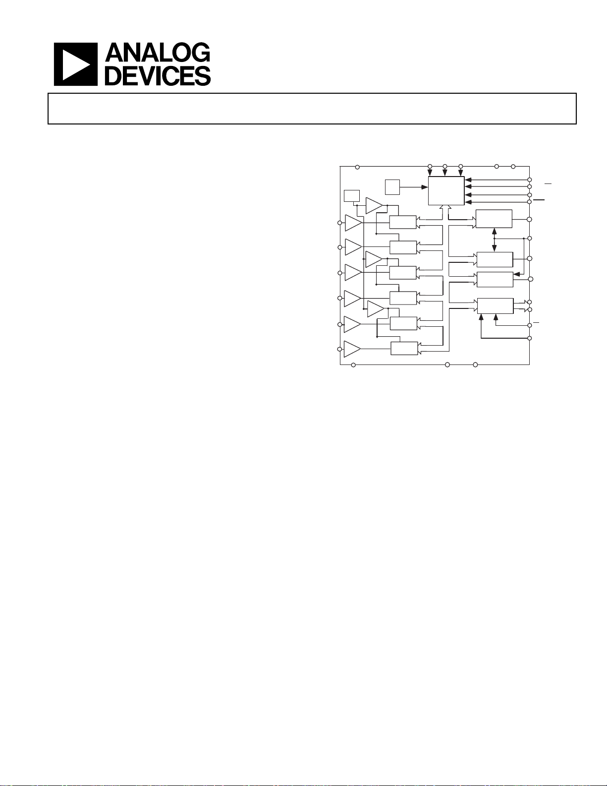
FUNCTIONAL BLOCK DIAGRAM
CONVSTB
DD
CONVSTA
CONVSTC
AV
DV
CC
CC
True Bipolar Analog Inputs
Pin/Software Selectable Ranges:- ±10V, ±5V
Fast throughput rate: 250 kSPS
Specified for AV
of 4.75 V to 5.25 V
CC
Low power
160mW at 250 kSPS with 5 V supplies
Wide input bandwidth:
85 dB SNR at 50 kHz input frequency
On-chip Reference and Reference Buffers
Parallel and Serial Interface
High speed serial interface
SPI/QSPI/µWire/DSP compatible
Standby mode: 5 µA max
TM
iCMOS
Process Technology
64 LQFP package
APPLICATIONS
Power Line Monitoring systems
CLK
REF
V
T/H
1
V
T/H
2
V
T/H
3
V
T/H
4
V
T/H
5
V
T/H
6
V
SS
OSC
BUF
16-BIT SAR
16-BIT SAR
BUF
16-BIT SAR
16-BIT SAR
BUF
16-BIT SAR
16-BIT SAR
CONTROL
LOGIC
AGND
DGND
OUTPUT
DRIVERS
OUTPUT
DRIVERS
OUTPUT
DRIVERS
OUTPUT
DRIVERS
AD7656
Figure 1.
+5
SER/PAR
V
DRIVE
STBY
D
A
OUT
SCLK
D
B
OUT
D
C
OUT
DATA/
CONTROL
LINES
4,
94
Instrumentation and control systems
Multi-axis positioning systems
GENERAL DESCRIPTION
The AD7658/AD7657/AD7656 contain six 12/14/16-bit, fast, low
power, successive approximation ADCs all in the one package.
The AD7658/AD7657/AD7656 core operates from a single 4.75
V to 5.25 V power supply and features throughput rates up to 250
kSPS. The parts contain low noise, wide bandwidth track-andhold amplifiers that can handle input frequencies up to 8 MHz.
The conversion process and data acquisition are controlled
using CONVST signals and an internal oscillator. Three
signals in the ±10V range and ±5V range . They contain a 2.5V
internal reference and can also accept an external reference. If a
3V external reference is applied to the VREF pin, the ADCs can
accommodate a true bipolar ±12V analog input range. V
supplies of ±12V are required for this ±12V input range.
V
SS
DD
and
PRODUCT HIGHLIGHTS
1. Six 12/14/16-bit 250 kSPS ADCs on board.
2. Six true bipolar high impedance analog inputs.
CONVST pins allow independent simultaneous sampling of the
three ADC pairs. The AD7658/AD7657/AD7656 have both a
high speed parallel and serial interface allowing the devices to
interface with microprocessors or DSPs. When in Serial
interface mode these parts have a Daisy Chain feature allowing
3. The AD7658/AD7657/AD7656 feature both a parallel and
a high speed serial interface.
multiple ADCs to connect to a single serial interface. The
AD7658/AD7657/AD7656 can accommodate true bipolar input
* Protected by U.S. Patent No. 6,731,232
TM
iCMOS
Process Technology
For analog systems designers within industrial/instrumentation equipment OEMs who need high performance ICs at higher-voltage levels, iCMOS is a technology platform
that enables the development of analog ICs capable of 30V and operating at +/- 15V supplies while allowing dramatic reductions in power consumption and package size, and
increased AC and DC performance.
Rev. Pr
Information furnished by Analog Devices is believed to be accurate and reliable.
However, no responsibility is assumed by Analog Devices for its use, nor for any
infringements of patents or other rights of third parties that may result from its use.
Specifications subject to change without notice. No license is granted by implication
or otherwise under any patent or patent rights of Analog Devices. Trademarks and
registered trademarks are the property of their respective owners.
One Technology Way, P.O. Box 9106, Norwood, MA 02062-9106, U.S.A.
Tel: 781.329.4700 www.analog.com
Fax: 781.326.8703 © 2005 Analog Devices, Inc. All rights reserved.

AD7658/AD7657/AD7656
TABLE OF CONTENTS
AD7658 Specifications..................................................................... 3
Preliminary Technical Data
ADC Transfer Function............................................................. 16
AD7657 Specifications..................................................................... 5
AD7656 Specifications..................................................................... 7
Timing Specifications....................................................................... 9
Absolute Maximum Ratings.......................................................... 10
ESD Caution................................................................................ 10
Pin Functional Descriptions ..................................................... 11
Terminology .................................................................................... 14
converter details.......................................................................... 15
Track-and-Hold Section........................................................ 15
Analog Input Section............................................................. 15
REVISION HISTORY
Revision PrK: Preliminary Version
interface section.......................................................................... 18
Parallel Interface (SER/
Software Selection of ADCs.................................................. 19
Changing the Analog Input Range(
Changing the Analog Input Range(
SERIAL INTERFACE (SER/
Serial Read Operation ........................................................... 21
Daisy-Chain Mode(DCEN =1, SER/
Standby/Partial Power Down Modes of Operation........... 24
Ordering Guide .......................................................................... 26
PA R
= 0) ......................................... 18
H
/S SEL=0)................ 20
H
/S SEL=1)................ 20
PA R
= 1)................................. 20
PA R
= 1) ................... 22
Rev. PrK| Page 2 of 26

Preliminary Technical Data
AD7658/AD7657/AD7656
AD7658 SPECIFICATIONS1
Table 1. AVCC = 4.75 V to 5.25 V, VDD = 4.75 V to 16.5 V, VSS = -4.75 V to -16.5V, DVCC = 4.75 V to 5.25 V, V
= 250 kSPS, VREF = 2.5V Internal/External, unless otherwise noted; TA = T
f
SAMPLE
MIN
to T
, unless otherwise noted
MAX
Parameter B Versions1 Unit Test Conditions/Comments
DYNAMIC PERFORMANCE fIN = 50 kHz sine wave
Signal-to-Noise + Distortion (SINAD)2 70 dB min
71 dB typ
Total Harmonic Distortion (THD) 2 −92 dB typ
Peak Harmonic or Spurious Noise (SFDR) 2 −-TBD dB typ
Intermodulation Distortion (IMD) 2
Second-Order Terms −94 dB typ
Third-Order Terms −100 dB typ
Aperture Delay 20 ns max
Aperature Delay Matching 2 ns max
100 ps typ
Aperture Jitter 30 ps typ
Full Power Bandwidth 8 MHz typ @ −3 dB
2.2 MHz typ @ −0.1 dB
DC ACCURACY
No Missing Codes 12 Bits min
Integral Nonlinearity2 ±1 LSB typ
Positive Full Scale Error2 ±0.4 % FS max
Bipolar Zero Error2 ±2.1 mV max VDD = 5.5 V
Negative Full Scale Error2 ±0.4 % FS max
ANALOG INPUT See Table 7 for min VDD/ VSS for each Range
Input Voltage Ranges ±4xVREF V RNG bit/RANGE pin = 0,
min V
& VSS = ±4xVREF
DD
±2xVREF V RNG bit/RANGE pin = 1,
min VDD & VSS = ±2xVREF
DC Leakage Current ±0.3 µA max
Input Capacitance 30 pF typ
REFERENCE INPUT/OUTPUT
Reference output voltage 2.49/2.51 V min/max
Reference input Voltage range 2.5/3 V min/max
DC Leakage current ±0.5 µA max V
REF
Pin
Input capacitance 20 pF typ
V
Output Impedance 1 kOhms typ
REF
Reference temperature Coefficient 25 ppm/°C max
10 ppm/°C typ
LOGIC INPUTS
Input High Voltage, V
Input Low Voltage, V
0.7 x V
INH
03 x V
INL
V min
DRIVE
V max
DRIVE
Input Current, IIN ±0.3 µA max Typically 10 nA, VIN = 0 V or VCC
Input Capacitance, C
3
10 pF max
IN
LOGIC OUTPUTS
Output High Voltage, VOH V
Output Low Voltage, VOL 0.4 V max I
– 0.2 V min I
DRIVE
= 200 µA;
SOURCE
= 200 µA
SINK
Floating-State Leakage Current ±0.3 µA max
Floating-State Output Capacitance3 10 pF max
Output Coding Two’s Complement
CONVERSION RATE
Conversion Time 3 µs max
Track-and-Hold Acquisition Time 400 ns max
Throughput Rate 250 kSPS
= 2.7V to 5.25V,
DRIVE
Rev. PrK | Page 3 of 26

AD7658/AD7657/AD7656
Preliminary Technical Data
Parameter B Versions1 Unit Test Conditions/Comments
POWER REQUIREMENTS
VDD +4.75V/+16.5V V min/max
VSS -4.75V/-16.5V V min/max
AVCC 4.75/5.25 V min/V max
DVCC
V
DRIVE
IDD Digital I/PS = 0 V or V
4.75/5.25 V min/V max
2.7/5.25 V min/V max
DRIVE
Normal Mode (Static) 40 mA max SCLK on or off. AVCC = 5.25 V
Normal Mode (Operational) 35 mA max f
= 250 kSPS. AVCC = 5.25 V
SAMPLE
Full Power-Down Mode 5 µA max SCLK on or off. AVCC = 5.25 V
Power Dissipation AVCC = 5.25 V
Normal Mode (Operational) 192.5 mW max f
= 250 kSPS
SAMPLE
Full Power-Down 16.5 µW max
1
Temperature range as follows: B Version: −40°C to +85°C.
2
See terminology section.
3
Sample tested during initial release to ensure compliance.
Rev. PrK| Page 4 of 26

Preliminary Technical Data
AD7658/AD7657/AD7656
AD7657 SPECIFICATIONS1
Table 2. AVCC = 4.75 V to 5.25 V, VDD = 4.75 V to 16.5 V, VSS = -4.75 V to -16.5V, DVCC = 4.75 V to 5.25 V, V
= 250 kSPS, VREF = 2.5V Internal/External, unless otherwise noted; TA = T
f
SAMPLE
MIN
to T
, unless otherwise noted
MAX
Parameter B Versions1 Unit Test Conditions/Comments
DYNAMIC PERFORMANCE fIN = 50 kHz sine wave
Signal-to-Noise + Distortion (SINAD2 81 dB min
Signal-to-Noise Ratio (SNR)2 82 dB min
83 dB typ
Total Harmonic Distortion (THD)2 −97 dB typ
Peak Harmonic or Spurious Noise (SFDR)2 −95 dB typ
Intermodulation Distortion (IMD)2
Second-Order Terms −94 dB typ
Third-Order Terms −100 dB typ
Aperture Delay 20 ns max
Aperature Delay Matching 2 ns max
100 ps typ
Aperture Jitter 30 ps typ
Full Power Bandwidth 8 MHz typ @ −3 dB
2.2 MHz typ @ −0.1 dB
DC ACCURACY
No Missing Codes 14 Bits min
Integral Nonlinearity2 ±1.5 LSB typ
Positive Full Scale Error2 ±0.4 % FS max
Bipolar Zero Error2 ±2.1 mV max VDD = 5.5 V
Negative Full Scale Error2 ±0.4 % FS max
ANALOG INPUT See Table 7 for min VDD/ VSS for each Range
Input Voltage Ranges ±4xVREF V RNG bit/RANGE pin = 0
±2xVREF V RNG bit/RANGE pin = 1
DC Leakage Current ±0.3 µA max
Input Capacitance 30 pF typ
REFERENCE INPUT/OUTPUT
Reference output voltage 2.49/2.51 V min/max
Reference input Voltage range 2.5/3 V min/max
DC Leakage current ±0.5 µA max V
REF
Pin
Input capacitance 20 pF typ
V
Output Impedance 1 kOhms typ
REF
Reference temperature Coefficient 25 ppm/°C max
10 ppm/°C typ
LOGIC INPUTS
Input High Voltage, V
Input Low Voltage, V
0.7 x V
INH
0.3 x V
INL
V min
DRIVE
V max
DRIVE
Input Current, IIN ±0.3 µA max Typically 10 nA, VIN = 0 V or VCC
Input Capacitance, C
3
10 pF max
IN
LOGIC OUTPUTS
Output High Voltage, VOH V
Output Low Voltage, VOL 0.4 V max I
– 0.2 V min I
DRIVE
= 200 µA;
SOURCE
= 200 µA
SINK
Floating-State Leakage Current ±0.3 µA max
Floating-State Output Capacitance 3 10 pF max
Output Coding Two’s Complement
CONVERSION RATE
Conversion Time 3 µs max
Track-and-Hold Acquisition Time 500 ns max
Throughput Rate 250 kSPS
POWER REQUIREMENTS
= 2.7V to 5.25V,
DRIVE
Rev. PrK | Page 5 of 26
AD7658/AD7657/AD7656
Preliminary Technical Data
Parameter B Versions1 Unit Test Conditions/Comments
VDD +4.75V/+16.5V V min/max
VSS -4.75V/-16.5V V min/max
AVCC 4.75/5.25 V min/V max
DVCC 4.75/5.25 V min/V max
V
2.7/5.25 V min/V max
DRIVE
IDD Digital I/PS = 0 V or V
DRIVE
Normal Mode (Static) 40 mA max SCLK on or off. VCC = 5.25 V
Normal Mode (Operational) 35 mA max f
= 250 kSPS. VCC = 5.25 V
SAMPLE
Full Power-Down Mode 5 µA max SCLK on or off. VCC = 5.25 V
Power Dissipation VCC = 5.25 V
Normal Mode (Operational) 192.5 mW max f
= 250 kSPS
SAMPLE
Full Power-Down 16.5 µW max
1
Temperature range as follows: B Version: −40°C to +85°C.
2
See Terminology Section.
3
Sample tested during initial release to ensure compliance.
Rev. PrK| Page 6 of 26

Preliminary Technical Data
AD7658/AD7657/AD7656
AD7656 SPECIFICATIONS1
Table 3. AVCC = 4.75 V to 5.25 V, VDD = 4.75 V to 16.5 V, VSS = -4.75 V to –16.5V, DVCC = 4.75 V to 5.25 V, V
= 250 kSPS, VREF = 2.5V Internal/External, unless otherwise noted; TA = T
f
SAMPLE
MIN
to T
, unless otherwise noted
MAX
Parameter B Versions1 Unit Test Conditions/Comments
DYNAMIC PERFORMANCE fIN = 50 kHz sine wave
Signal-to-Noise + Distortion (SINAD)2 82.5 dB min
85 dB typ
Signal-to-Noise Ratio (SNR)2 83 dB min
86 dB typ
Total Harmonic Distortion (THD)2 −97 dB max
Peak Harmonic or Spurious Noise (SFDR)2 −95 dB typ
Intermodulation Distortion (IMD)2
Second-Order Terms −94 dB typ
Third-Order Terms −100 dB typ
Aperture Delay 20 ns max
Aperature Delay Matching 2 ns max
100 ps typ
Aperture Jitter 30 ps typ
Full Power Bandwidth 8 MHz typ @ −3 dB
2.2 MHz typ @ −0.1 dB
DC ACCURACY
No Missing Codes 15 Bits min
Integral Nonlinearity2 ±2 LSB typ
±4 LSB max
Positive Full Scale Error2 ±0.4 % FS max
Bipolar Zero Error2 ±2.1 mV max VDD = 5.5 V
Negative Full Scale Error2 ±0.4 % FS max
ANALOG INPUT See Table 7 for min VDD/ VSS for each Range
Input Voltage Ranges ±4xVREF V RNG bit/RANGE pin = 0
±2xVREF V RNG bit/RANGE pin = 1
DC Leakage Current ±0.3 µA max
Input Capacitance 30 pF typ
REFERENCE INPUT/OUTPUT
Reference output voltage 2.49/2.51 V min/max
Reference input Voltage range 2.5/3 V min/max
DC Leakage current ±0.5 µA max V
REF
Pin
Input capacitance 20 pF typ
V
Output Impedance 1 kOhms typ
REF
Reference temperature Coefficient 25 ppm/°C max
10 ppm/°C typ
LOGIC INPUTS
Input High Voltage, V
Input Low Voltage, V
0.7 x V
INH
0.3 x V
INL
V min
DRIVE
V max
DRIVE
Input Current, IIN ±0.3 µA max Typically 10 nA, VIN = 0 V or VCC
Input Capacitance, C
3
10 pF max
IN
LOGIC OUTPUTS
Output High Voltage, VOH V
Output Low Voltage, VOL 0.4 V max I
– 0.2 V min I
DRIVE
= 200 µA;
SOURCE
= 200 µA
SINK
Floating-State Leakage Current ±0.3 µA max
Floating-State Output Capacitance
, 3
10 pF max
Output Coding Two’s Complement
CONVERSION RATE
Conversion Time 3 µs max
Track-and-Hold Acquisition Time 1 µs max
Throughput Rate 250 kSPS
= 2.7V to 5.25V,
DRIVE
Rev. PrK | Page 7 of 26

AD7658/AD7657/AD7656
Preliminary Technical Data
Parameter B Versions1 Unit Test Conditions/Comments
POWER REQUIREMENTS
VDD +4.75V/+16.5V V min/max
VSS -4.75V/-16.5V V min/max
AV
CC
DV
CC
V
DRIVE
IDD Digital I/PS = 0 V or V
4.75/5.25 V min/V max
4.75/5.25 V min/V max
2.7/5.25 V min/V max
DRIVE
Normal Mode (Static) 40 mA max SCLK on or off. VCC = 5.25 V
Normal Mode (Operational) 35 mA max f
= 250 kSPS. VCC = 5.25 V
SAMPLE
Full Power-Down Mode 5 µA max SCLK on or off. VCC = 5.25 V
Power Dissipation VCC = 5.25 V
Normal Mode (Operational) 192.5 mW max f
= 250 kSPS
SAMPLE
Full Power-Down 16.5 µW max
1
Temperature range as follows: B Version: −40°C to +85°C.
2
See terminology section.
3
Sample tested during initial release to ensure compliance.
V
Rev. PrK| Page 8 of 26

Preliminary Technical Data
AD7658/AD7657/AD7656
TIMING SPECIFICATIONS1
Table 4. AVCC /DVCC= 4.75 V to 5.25 V, VDD = 4.75 V to 16.5 V, VSS = -4.75 V to -16.5V, V
unless otherwise noted
Limit at T
MIN, TMAX
Parameter 5 V Unit Description
Parallel Mode
t
3 µs typ Conversion Time, Internal Clock
CONVERT
t
400 ns min Minimum quiet time required between bus relinquish and start of next conversion
QUIET
t1 3 ns min CONVST high to BUSY high
T
TBD ns typ
wake-up
STBY
rising edge to CONVST rising edge
Write Operation
t13 0 ns min
t14 0 ns min
t12 20 ns min
t15 5 ns min
t
5 ns min
12/14/16
CS
to WR setup time
CS
to WR Hold time
WR
Pulse width
Data setup time before WR rising edge
Data hold after WR rising edge
Read Operation
t2 0 ns min
t3 0 ns min
t4 0 ns min
t5 30 ns min
t6 30 ns max
t7 15 ns min
BUSY to RD Delay
CS
to RD setup time
CS
to RD Hold time
RD
Pulse width
Data access time after RD falling edge
Bus relinquish time after RD rising edge
25 ns max
t9 20 ns min Minimum time between reads
Serial Interface
f
20 MHz max Frequency of Serial Read Clock
SCLK
t17 10 ns max
t18 15 ns max
CS to SCLK setup time
Delay from CS until SDATA three-state disabled
t19 20 ns max Data access time after SCLK rising edge
t20 0.4 t
t21 0.4 t
ns min SCLK low pulse width
SCLK
ns min SCLK high pulse width
SCLK
t22 5 ns min SCLK to data valid hold time
t23 30 ns max
CS
rising edge to SDATA high impedance
= 2.7V to 5.25V; TA = T
DRIVE
MIN
to T
MAX
,
I
200µA
TO OUTPUT
Figure 2. Load Circuit for Digital Output Timing Specification
PIN
25pF
C
L
200µA
OL
1.6V
I
OH
1
Sample tested during initial release to ensure compliance. All input signals are specified with tr = tf = 5 ns (10% to 90% of VDD) and timed from a voltage level of 1.6 V.
Rev. PrK | Page 9 of 26

AD7658/AD7657/AD7656
Preliminary Technical Data
ABSOLUTE MAXIMUM RATINGS
Table 5. TA = 25°C, unless otherwise noted
Parameter Rating
VDD to AGND, DGND -0.3 V to +16.5 V
VSS to AGND, DGND +0.3 V to –16.5 V
AVCC to AGND, DGND -0.3V to +7V
DVCC to AVCC -0.3 V to + 0.3V
DVCC to DGND -0.3 V to + 7V
AGND to DGND -0.3 V to +0.3 V
V
to DGND -0.3 V to +DVCC + 0.3V
DRIVE
Analog Input Voltage to AGND VSS – 0.5V to VDD + 0.5V
Digital Input Voltage to DGND -0.3 V to V
Digital Output Voltage to GND -0.3 V to V
REFIN to AGND -0.3 V to AVCC +0.3V
Input Current to Any Pin Except Supplies
Operating Temperature Range -40°C to +85°C
Storage Temperature Range -65°C to +150°C
Junction Temperature +150°C
64-LQFP Package, Power Dissipation
θJA Thermal Impedance TBD°C/W
θJC Thermal Impedance TBD°C/W
Pb-free Temperature, Soldering
Reflow 260(+0)°C
ESD TBD kV
1
Transient currents of up to 100 mA will not cause SCR latch-up.
2
Stresses above those listed under Absolute Maximum Ratings
may cause permanent damage to the device. This is a stress
rating only; functional operation of the device at these or any
other conditions above those listed in the operational sections
of this specification is not implied. Exposure to absolute
maximum rating conditions for extended periods may affect
device reliability.
DRIVE
DRIVE
+0.3 V
+0.3V
±10mA
ESD CAUTION
ESD (electrostatic discharge) sensitive device. Electrostatic charges as high as 4000 V readily accumulate on the
human body and test equipment and can discharge without detection. Although this product features
proprietary ESD protection circuitry, permanent damage may occur on devices subjected to high energy
electrostatic discharges. Therefore, proper ESD precautions are recommended to avoid performance
degradation or loss of functionality.
Rev. PrK| Page 10 of 26

Preliminary Technical Data
PIN FUNCTIONAL DESCRIPTIONS
EN/DIS
AD7658/AD7657/AD7656
DB14/REFBUF
DB10/SDATA C
DB9/SDATA B
DB8/SDATA A
VDRIVE
DB7/HBEN/DCEN
DB6/SCLK
DB5/DCIN A
DB4/DCIN B
DB3/DCIN C
DB2/SEL C
DB1/SEL B
EN/DIS
DB13
DB12
DB11
DGND
WR/REF
63
H/S SEL
62
DB15
64
PIN 1
1
IDENTIFIER
2
3
4
5
6
7
8
9
10
11
12
13
14
15
16
AVCC
SER/PAR SEL
61
60
AGND
59
AGND
REFCAPC
58
57
56
AD7656
TOP VIEW
(Not to Scale)
AGND
REFCAPB
55
AVCC
AGND
AGND
REFCAPA
53
54
52
AGND
REFIN/REFOUT
49
50
51
48
47
46
45
44
43
42
41
40
39
38
37
36
35
34
33
V6
AVCC
AVCC
V5
AGND
AGND
V4
AVC C
AVC C
V3
AGND
AGND
V2
AVCC
AVCC
V1
17
18
BUSY
DB0/SEL A
19
CS
21
20
RD
CONVST C
23
22
CONVST B
CONVST A
24
STBY
DGND
Table 6. AD7658/AD7657/AD7656 Pin Function Descriptions
Pin Mnemonic Description
REFCAPA, REFCAPB,
REFCAPC
V1 – V6
AGND
DVCC
V
DRIVE
Rev. PrK | Page 11 of 26
Decoupling capacitors are connected to these pins to decouple the reference buffer for each
ADC pair. Each REFCAP pin should be decoupled to AGND using 10 µF and 100 nF capacitors.
Analog Input1-6. These are six single-ended Analog inputs. The Analog input range on these
channels is ddetermined by the RANGE pin.
Analog Ground. Ground reference point for all analog circuitry on the
AD7658/AD7657/AD7656. All analog input signals and any external reference signal should be
referred to this AGND voltage. All eleven of these AGND pins should be connected to the
AGND plane of a system. The AGND and DGND voltages ideally should be at the same
potential and must not be more than 0.3 V apart, even on a transient basis.
Digital Power. Normally at 5V. The DVCC and AVCC voltages should ideally be at the same
potential and must not be more than 0.3 V apart even on a transient basis. This supply should
be decoupled to DGND. 10 µF and 100 nF decoupling capacitors should be placed on the
DVCC pin.
Logic power supply input. The voltage supplied at this pin determines at what voltage the
interface will operate. Nominally at the same supply as the supply of the host interface. This
25
26
DVCC
27
RANGE
29
28
W/B
RESET
30
VSS
31
VDD
32
AGND

AD7658/AD7657/AD7656
pin should be decoupled to DGND. 10 µF and 100 nF decoupling capacitors should be placed
pin.
DRIVE
H
/S SEL = 0 and REF EN/
DGND
AVCC
CONVSTA, B, C
CS
RD
PAR
DISABLE
WR
/ REF EN/
BUSY
REFIN/REFOUT
SER/
DB[0]/SEL A
DB[1]/SEL B
DB[2]/SEL C
DB[3]/DCIN C
DB[4]/DCIN B
DB[5]/DCIN A
on the V
Digital Ground. This is the ground reference point for all digital circuitry on the
AD7658/AD7657/AD7656. Both DGND pins should connect to the DGND plane of a system.
The DGND and AGND voltages ideally should be at the same potential and must not be more
than 0.3 V apart even on a transient basis.
Analog Supply Voltage, 4.5 V to 5.5 V. This is the only supply voltage for ADC cores. The AVCC
and DVCC voltages ideally should be at the same potential and must not be more than 0.3 V
apart even on a transient basis. This supply should be decoupled to AGND. 10 µF and 100 nF
decoupling capacitors should be placed on the AVCC pins.
Conversion Start Input A,B,C. Logic Inputs. These inputs are used to initiate conversions on the
ADC pairs. CONVSTA is used to initiate simultaneous conversions on V1 and V2. CONVSTB is
used to initiate simultameous conversions on V3 and V4. CONVSTC is used to initiate
simultaneous conversions on V5 and V6. When CONVSTX switches from low to high the trackand-hold switch on the selected ADC pairs switches from track to hold and the conversion is
initiated.
Chip Select. Active low logic input. This input frames the data transfer. When both
are logic low in parallel mode the output bus is enabled and the conversion result is output on
the Parallel Data Bus lines. When both
used to write data to the on-chip control register. In serial mode the
serial read transfer.
Read Data. When both
serial Mode the RD line should be held low.
Write Data/ reference Enable/Disable. When H/S SEL pin is high both CS and WR are logic low
DB[15:8] are used to write data to the internal Control Register. When
pin is used to enable or disable the internal Reference. When
0 the internal reference is disabled and an external reference should be applied to this pin.
When
BUSY Output. Transitions high when a conversion is started and remains high until the
conversion is complete and the conversion data is latched into the Output Data registers.
Reference Input/Output. The on-chip reference is available on this pin for use external to the
AD7658/AD7657/AD7656. Alternatively, the internal reference can be disabled and an external
reference applied to this input. See Reference Section.
Serial/parallel selection Input. When low, the parallel port is selected. When high the serial
interface mode is selected. In serial mode DB[10:8] take on their SDATA [C:A] function, DB[0:2]
take on their DOUT select function, DB[7] takes on its DCEN function. In serial mode DB15 and
DB[13:11] should be tied to DGND.
Data Bit [0]/Select DOUT A. When SER/
Output pin. When SER/
serial interface. If this pin is 1, the serial interface will operate with one/two/three DOUT ouput
pins and enables DOUT A as a serial output. When operating in serial mode this pin should
always be = 1.
Data Bit [1]/Select DOUT B. When SER/
Output pin. When SER/
serial interface. If this pin is 1, the serial interface will operate with two/three DOUT ouput pins
and enables DOUT B as a serial output. If this pin is 0 the DOUT B is not enabled to operate as a
serial Data Output pin and only one DOUT output pin is used.
Data Bit [2]/Select DOUT C. When SER/
Output pin. When SER/
serial interface. If this pin is 1, the serial interface will operate with three DOUT ouput pins and
enables DOUT C as a serial output. If this pin is 0 the DOUT C is not enabled to operate as a
serial Data Output pin.
Data Bit [3]/Daisy Chain in C. When SER/
Output pin. When SER/
Data Bit [4]/Daisy Chain in B. When SER/
Output pin. When SER/
Data Bit [5]/Daisy Chain in A. When SER/
Preliminary Technical Data
CS
and RD
CS
and WR are logic low in parallel mode DB[15:8] are
CS
is used to frame the
CS
and RD are logic low in parallel mode the output bus is enabled. In
H
/S SEL pin is low this
H
/S SEL =0 and REF EN/
DISABLE
PAR
is =1, this pin takes on its SEL A function, it is used to configure the
PAR
is =1, this pin takes on its SEL B function, it is used to configure the
PAR
is =1, this pin takes on its SEL C function, it is used to configure the
PAR
is =1 and DCEN = 1, this pin acts as Daisy Chain Input C.
PAR
is =1 and DCEN = 1, this pin acts as Daisy Chain Input B.
= 1 the internal reference is enabled.
PAR
= 0, this pin acts as a three-state Parallel Digital
PAR
= 0, this pin acts as a three-state Parallel Digital
PAR
= 0, this pin acts as a three-state Parallel Digital
PAR
=0, this pin acts as a three-state Parallel Digital
PAR
=0, this pin acts as a three-state Parallel Digital
PAR
is low, this pin acts as a three-state Parallel Digital
DISABLE
=
Rev. PrK| Page 12 of 26

Preliminary Technical Data
Output pin. When SER/
DB[6]/SCLK
DB[7]/HBEN/DCEN
DB[8]/DOUT A
DB[9]/DOUT B
DB[10]/DOUT C
DB[11]/DGND
DB[12:13], DB[15]
DB[14]/REFBUF EN
/DIS
RESET
RANGE
VDD
VSS
STBY
H
/S SEL Hardware/Software Select Input. Logic Input. When SER/
W
/B
Data Bit [6[/Serial Clock. When SER/
pin. When SER/
for the serial transfer.
Data bit 7/ High Byte Enable/ Daisy Chain Enable. When operating in Parallel Word mode
PAR
(SER/
Byte mode (SER/
and the HBEN pin is a logic high, the data will be output MSB byte first on DB[15:8]. When the
HBEN pin is a logic low the data will be output LSB byte first on DB[15:8]. When operating in
Serial mode (SER/
the part will operate in Daisy Chain mode with DB[5:3] taking on their DCIN[A:C] function.
Data Bit [8]/Serial Data Output A. When SER/
Digital Output pin. When SER/
Data Bit [9]/Serial Data Output B. When SER/
Digital Output pin. When SER/
configures the serial interface to have two SDATA output lines.
Data Bit [10]/Serial Data Output C. When SER/
Digital Output pin. When SER/
configures the serial interface to have three SDATA output lines.
Data Bit [11]/Digital Ground. When SER/
Output pin. When SER/
Data Bit [12:15]. SER/
When
are low these pins are used to write to the Control Register. When SER/
should be tied to DGND.
Data Bit [14]/ REFBUF ENABLE/
Input/output pin. When SER/
reference buffers.
Reset Input. When set to a logic high, reset the AD7658/AD7657/AD7656. The Current
conversion if any is aborted. Internal register is set to all 0’s. If not in use, this pin could be tied
low. In Hardware mode the AD7658/AD7657/AD7656 will be configured depending on the
logic levels on the hardware select pins. When operating in software mode a reset pulse is
required afterpower up to select the default settings in the Internal register. (See Register
section)
Analog Input Range Selection. Logic input. The polarity on this pin will determine what input
range the analog input channels will have. When this pin is a logic 1 at the falling edge of
BUSY then range for the next conversion is ± 2 x VREF. When this pin is a logic 0 at the falling
edge of BUSY then range for the next conversion is ± 4 x VREF.
Positive power supply voltage. This is the positive supply voltage for the Analog Input section.
10 µF and 100 nF decoupling capacitors should be placed on the VDD pin.
Negative power supply voltage. This is the negavtive supply voltage for the Analog Input
section. 10 µF and 100 nF decoupling capacitors should be placed on the VSS pin.
Standby mode Input. This pin is used to put all six on-chip ADCs into standby mode. The
pin is high for normal operation and low for standby operation.
AD7658/AD7657/AD7656 operates in Hardware select mode. The ADC pairs to be
simultaneously sampled are selected by the
high the ADC pairs to be simultaneously sampled are selected by writing to the control
register.
Word/Byte Input. When this pin is a logic low data can be transfered to and from the
AD7658/AD7657/AD7656 using the parallel data lines DB[15:0]. When this pin is a logic high
Byte mode is enabled. In this mode data is transferred using data lines DB[15:8], DB[7] takes on
its HBEN function. To obtain the 12/14/16-bit conversion result two byte reads are required.
= 0 and W/B = 1) this pin takes on its Data bit 7 function. When operating in Parallel
CS
and RD are low these pins are used to output the conversion result. When CS and WR
PAR
is =1 and DCEN = 1, this pin acts as Daisy Chain Input A.
PAR
=0, this pin acts as three-state Parallel Digital Output
PAR
=1 this pin takes on its SCLK input function, obtaining the read serial clock
PAR
= 0 and W/B = 0), this pin takes on its HBEN function. When in this mode
PAR
= 1) this pin takes on its DCEN function. When DCEN pin is a logic high
PAR
=0, this pin acts as a three-state Parallel
PAR
=1 and SEL A = 1, this pin takes on its DOUT A function.
PAR
=0, this pin acts as a three-state Parallel
PAR
=1 and SEL B = 1, this pin takes on its DOUT B function. This
PAR
=0, this pin acts as a three-state Parallel
PAR
=1 and SEL C = 1, this pin takes on its DOUT C function. This
PAR
=0, this pin acts as a three-state Parallel Digital
PAR
=1, this pin should be tied to DGND.
PAR
=0 these pins act as a three-state parallel Digital Input/Output pins.
DISABLE
PAR
. When SER/
=1, this pin can be used to enable or disable the internal
CONVST
AD7658/AD7657/AD7656
PAR
=1 these pins
PAR
=0, this pin acts as a three-state Digital
PAR
=0 and this pin is a logic low the
pins. When SER/
PAR
=0 this pin is a logic
STBY
Rev. PrK | Page 13 of 26

AD7658/AD7657/AD7656
TERMINOLOGY
Integral Nonlinearity
This is the maximum deviation from a straight line passing
through the endpoints of the ADC transfer function. The
endpoints of the transfer function are zero scale, a point 1/2 LSB
below the first code transition, and full scale, a point 1/2 LSB
above the last code transition.
Preliminary Technical Data
2
2
2
2
2
=
dBTHD
2
log20)(
4
3
V
1
where V1 is the rms amplitude of the fundamental and V2, V3,
V
, V5, and V6 are the rms amplitudes of the second through the
4
sixth harmonics.
++++
VVVVV
6
5
Differential Nonlinearity
This is the difference between the measured and the ideal 1 LSB
change between any two adjacent codes in the ADC.
Bipolar Zero Code Error
It is the deviation of the midscale transition (all 1s to all 0s)
from the ideal V
voltage, i.e., AGND - 1 LSB.
IN
Positive Full Sc ale Error
It is the deviation of the last code transition (011…110) to
(011…111) from the ideal ( +4 x V
- 1 LSB, + 2 x V
REF
LSB) after the bipolar Zero Code Error has been adjusted out.
REF
– 1
Negative Full Scale Error
This is the deviation of the first code transition (10…000) to
(10…001) from the ideal (i.e., - 4 x V
+ 1 LSB, - 2 x V
REF
LSB) after the Bipolar Zero Code Error has been adjusted out.
REF
+ 1
Track-and-Hold Acquisition Time
The track-and-hold amplifier returns to track mode at the end
of conversion. The track-and-hold acquisition time is the time
required for the output of the track-and-hold amplifier to reach
its final value, within ±1 LSB, after the end of the conversion.
See the
Track-and-Hold Section for more details.
Signal-to-(Noise + Distortion) Ratio
This is the measured ratio of signal-to-(noise + distortion) at
the output of the ADC. The signal is the rms amplitude of the
fundamental. Noise is the sum of all nonfundamental signals up
to half the sampling frequency (f
/2, excluding dc). The ratio
S
depends on the number of quantization levels in the digitization
process; the more levels, the smaller the quantization noise. The
theoretical signal-to-(noise + distortion) ratio for an ideal N-bit
converter with a sine wave input is given by
Signal-to-(Noise + Distortion) = (6.02 N + 1.76) dB
Thus, for a 12-bit converter, this is 74 dB, for a 14-bit converter,
this is 86 dB and for a 16-bit converter, this is 98 dB.
Total Harmonic Distortion (THD)
THD is the ratio of the rms sum of harmonics to the
fundamental. For the AD7658/AD7657/AD7656, it is defined as
Peak Harmonic or Spurious Noise
Peak harmonic or spurious noise is defined as the ratio of the
rms value of the next largest component in the ADC output
spectrum (up to f
/2, excluding dc) to the rms value of the
S
fundamental. Normally, the value of this specification is
determined by the largest harmonic in the spectrum, but for
ADCs where the harmonics are buried in the noise floor, it will
be a noise peak.
Intermodulation Distortion
With inputs consisting of sine waves at two frequencies, fa and fb,
any active device with nonlinearities will create distortion
products at sum and difference frequencies of mfa ± nfb where m,
n = 0, 1, 2, 3. Intermodulation distortion terms are those for which
neither m nor n are equal to zero. For example, the second-order
terms include (fa + fb) and (fa − fb), while the third-order terms
include (2fa + fb), (2fa − fb), (fa + 2fb), and (fa −2fb).
The AD7658/AD7657/AD7656 is tested using the CCIF
standard where two input frequencies near the top end of the
input bandwidth are used. In this case, the second-order terms
are usually distanced in frequency from the original sine waves,
while the third-order terms are usually at a frequency close to
the input frequencies. As a result, the second- and third-order
terms are specified separately. The calculation of the
intermodulation distortion is as per the THD specification
where it is the ratio of the rms sum of the individual distortion
products to the rms amplitude of the sum of the fundamentals
expressed in dBs.
Rev. PrK| Page 14 of 26

Preliminary Technical Data
CONVERTER DETAILS
The AD7658/AD7657/AD7656 are high-speed, low power
converters that allow the simultaneous sampling of their six onchip ADCs. The Analog Inputs on the
AD7658/AD7657/AD7656 can accept True bipolar Input
signals, the RANGE pin/RNG bits are used to select between ±4
x VREF or ±2 x VREF as the Input Range for the next
conversion.
The AD7658/AD7657/AD7656 contain six SAR ADCs, six
track-and-hold amplifiers, on-chip 2.5V reference, reference
buffers, high speed parallel and serial interfaces. The
AD7658/AD7657/AD7656 allow the simultaneous sampling of
all six ADCs when all three CONVST signals are tied together.
Alternatively the six ADCs can be grouped into three pairs.
Each pair has an associated CONVST signal used to initiate
simultaneous sampling on each ADC pair, on four ADCs or all
six ADCs. CONVSTA is used to initiate simultaneous sampling
on V1 and V2, CONVSTB is used to initiate simultaneous
sampling on V3 and V4, and CONVSTC is used to initiate
simultaneous sampling on V5 and V6.
A conversion is initiated on the AD7658/AD7657/AD7656 by
pulsing the CONVSTX input. On the rising edge of CONVSTX
the track-and-hold on the selected ADCs will be placed into
hold mode and the conversions are started. After the rising edge
of CONVSTX the BUSY signal will go high to indicate the
conversion is taking place. The conversion clock for the part is
internally generated and the conversion time for the
AD7658/AD7657/AD7656 is 3 µs from the rising edge of
CONVSTX. The BUSY signal will return low to indicate the end
of conversion. On the falling edge of BUSY the track-and-hold
will return to track mode. Data can be read from the output
register via the parallel or serial interface.
Track-and-Hold Section
The track-and-Hold amplifiers on the
AD7658/AD7657/AD7656 allow the ADCs to accurately
convert an input sine wave of full-scale amplitude to 12/14/16bit resolution. The input bandwidth of the track-and-hold
amplifiers is greater that the Nyquist rate of the ADC even
when the AD7658/AD7657/AD7656 is operating at its
maximum throughput rate. The AD7658/AD7657/AD7656 can
handle input frequencies up to 8 MHz.
The track-and-hold amplifiers sample their respective inputs
simultaneously on the rising edge of CONVSTX. The aperture
time for the track-and-hold, (i.e. the delay time between the
external CONVSTX signal actually going into hold), is typically
20ns. This is well matched across all six track-and-holds on the
one device and also from device to device. This allows more
AD7658/AD7657/AD7656
than six ADCs to be simultaneously sampled. The end of the
conversion is signaled by the falling edge of BUSY and its at this
point the track-and-holds return to track mode and the
acquisition time begins.
Analog Input Section
The AD7658/AD7657/AD7656 can handle True bipolar input
voltages. The logic level on the RANGE pin or the value written
to the RNGX bits in the Control register will determine the
Analog input Range on the AD7658/AD7657/AD7656 for the
next conversion. When the RANGE pin/ RNGX bit is 1 the
Analog input range for the next conversion is ±2 x VREF, when
the RANGE pin/ RNG bit is 0 the Analog Input range for the
next conversion is ±4 x VREF.
V
DD
D
V1
Figure 3. Equivalent Analog Input Structure
C1
D
V
SS
Figure 3 shows an equivalent circuit of the analog input
structure of the AD7658/AD7657/AD7656. The two diodes, D1
and D2, provide ESD protection for the analog inputs. Care
must be taken to ensure that the analog input signal never
exceeds the V
and VSS supply rails by more than TBD mV.
DD
This will cause these diodes to become forward-biased and to
start conducting current into the substrate. The maximum
current these diodes can conduct without causing irreversible
damage to the part is 10 mA. Capacitor C1 in Figure 3 is
typically about 5 pF and can be attributed primarily to pin
capacitance. Resistor R1 is a lumped component made up of the
on resistance of a switch (track-and-hold switch). This resistor
is typically about 25 Ω. Capacitor C2 is the ADC sampling
capacitor and has a capacitance of 25 pF typically.
The AD7656/7/8 require V
DD
and V
dual supplies for the high
SS
voltage Analog input structures. These supplies must be equal to
or greater than the Analog input range. See Table 7 for the
requirements on these supplies for each Analog Input Range.
The AD7656/7/8 require a low voltage 4.75V to 5.25 V AV
supply to power the ADC core, a 4.75V to 5.25V DV
for the Digital Power and a 2.7V to 5.25V V
DRIVE
interface power.
To meet the specified performance when using the minimum
supply voltage for the selected analog input range it maybe
necessary to reduce the throughput rate from the maximum
throughput rate.
C2R1
CC
supply
CC
supply for the
Rev. PrK | Page 15 of 26

AD7658/AD7657/AD7656
Preliminary Technical Data
Table 7. Minimum VDD/VSS Supply Volage Requirements
Analog Input Range (V) Reference Voltage (V) Full Scale Input (V) Minimum VDD/VSS (V)
±4xVREF 2.5 ±10 ±10
±4xVREF 3.0 ±12 ±12
±2xVREF 2.5 ±5 ±5
±2xVREF 3.0 ±6 ±6
ADC TRANSFER FUNCTION
The output coding of the AD7658/AD7657/AD7656 is two’s
Complement. The designed code transitions occur midway
between successive integer LSB values, i.e., 1/2 LSB, 3/2 LSBs.
The LSB size is FSR/4096 for the AD7658, FSR/16384 for the
AD7657 and FSR/65536 for the AD7656. The ideal transfer
characteristic for the AD7658/AD7657/AD7656 is shown in
Figure 4.
011...111
011...110
000...001
000...000
111...111
ADC CODE
100...010
100...001
100...000
-
FSR/2 +
1/2LSB
Figure 4. AD7658/AD7657/AD7656 Transfer Characteristic
AGND - 1LSB
ANAL OG INPUT
+FSR /2 3/2LSB
The LSB size is dependant on the Analog Input Range selected.
See Table 8.
source for the AD7658/AD7657/AD7656 conversions. The
AD7658/AD7657/AD7656 can accommodate a 2.5V to 3V
external reference range. When using an external reference the
internal reference needs to be disabled. After a RESET the
AD7658/AD7657/AD7656 defaults to operating in external
Reference mode with the internal reference buffers enabled. The
internal reference can be enabled in either hardware or software
mode. To enable the internal reference in hardware mode,
SEL pin =0 and the REF EN/
DISABLE
internal reference in software mode
= 1. To enable the
H
/S SEL pin =1, a write to
H
/S
the control register is necessary to make DB1 of the register = 1.
The REFIN/OUT pin should be decoupled using 10 µF and 100
nF capacitors.
The AD7656 contains three on-chip reference buffers. Each of
the three ADC pairs has an associated reference buffer. These
reference buffers require external decoupling caps on REF
REF
B, and REF
CAP
capacitor should be placed on these REF
C pins. 10 µF and 100 nF decoupling
CAP
pins. The internal
CAP
CAP
A,
reference buffers can be disabled by writing to bit B8 in the
internal control register. If operating in serial mode the internal
reference buffers can be disabled by setting DB14/REFBUF
ENABLE
/DISABLE pin high.
REFERENCE SECTION
The VREF pin either provides access to the
AD7658/AD7657/AD7656’s own 2.5V reference or allows for an
external reference to be connected providing the reference
Table 8. LSB sizes for each Analog Input Range
AD7656 AD7657 AD7658
Input Range
±10V ±5V ±10V ±5V ±10V ±5V
FS Range 20V/65536 10V/65536 20V/16384 10V/16384 20V/4096 10V/4096
LSB Size 0.305 mV 0.152 mV 1.22 mV 0.61 mV 4.88 mV 2.44 mV
Rev. PrK| Page 16 of 26

Preliminary Technical Data
AD7658/AD7657/AD7656
Analog Supply
Voltage 5V
Note 1
+9.5V to +16.5V
Supply
2.5V
REF
10 µF
10 µF
10 µF
-9.5V to -16.5V
Supply
+
+
+
Six Analog
Inputs
10 µF
+
10 µF
100 nF
100 nF
100 nF
100 nF
+
AGND
VDD
AGND
REFCAPA/B/C
AGND
REFIN/OUT
AGND
VSS
AGND
100 nF
AVC C
DVCC
10 µF+
100 nF
DGND
DVCC
AD7658/7/6
100 nF
VDRIVE DGND
D0 to D15
CONVST A/B/C
CS
RD
BUSY
SER/PAR
H/S
W/B
RANGE
RESET
STDBY
Digital Supply
Voltage 3V or 5V
+
10 µF
PARALLEL
INTERFACE
VDRIVE
µP/µC/DSP
Note 1: Decoupling shown on the
AV
pin applies to each AVCC pin.
CC
Figure 5. AD7658/AD7657/AD7656 Typical connection diagram.
Rev. PrK | Page 17 of 26

AD7658/AD7657/AD7656
INTERFACE SECTION
The AD7658/AD7657/AD7656 provides two interface options,
a parallel interface and a high speed serial interface. The
required interface mode is selected via the SER/
parallel interface can operate in word (
W
1) mode. The interface modes are discussed in the following
sections.
Parallel Interface (SER/
PAR
= 0)
The AD7658/AD7657/AD7656 consist of six 12/14/16-bit
ADCs. A simultaneous sample of all six ADCs can be
performed by connecting all three CONVST pins together,
CONVSTA, CONVSTB, CONVSTC. The rising edge of
CONVSTX initiates simultaneous conversions on the selected
ADCs. The AD7658/AD7657/AD7656 contains an on-chip
oscillator that is used to perform the conversions. The
conversion time, t
is 3 µs. The BUSY signal goes low to
CONV,
indicate the End of Conversion. The falling edge of the BUSY
signal is used to place the track-and-hold into track mode. The
AD7658/AD7657/AD7656 also allow the six ADCs to be
simultaneously converted in pairs by pulsing the three
CONVST pins independently. CONVSTA is used to initiate
simultaneous conversions on V1 and V2, CONVSTB is used to
initiate simultaneous conversions on V3 and V4, and
CONVSTC is used to initiate simultaneous conversions on V5
and V6. The conversion results from the simultaneously
sampled ADCs are stored in the output data registers.
Data can be read from the AD7658/AD7657/AD7656 via the
parallel data bus with standard
CS
and RD signals (W/B = 0).
To read the data over the parallel bus SER/
CS
low. The
and RD input signals are internally gated to enable
the conversion result onto the data bus. The data lines DB0 to
DB15 leave their high impedance state when both
CS
are logic low. The
RD
the
signal can be used to access the conversion results. A
signal can be permanently tied low and
read operation can take place after the BUSY signal goes low.
PA R
pin. The
/B= 0) or byte (W/B =
PA R
should be tied
CS
and RD
Preliminary Technical Data
The number of read operations required will depend on the
number of ADCs that were simultaneously sampled, see Figure
5. If CONVSTA and CONVSTB were brought low
simultaneously, four read operations are required to obtain the
conversion results from V1, V2, V3 and V4. The conversion
results will be output in ascending order. For the AD7657 DB15
and DB14 will contain two leading zeros and DB[13:0] will
output the 14-bit conversion result. For the AD7658 DB[15:12]
will contain four leading zeros and DB[11:0] will output the 12bit conversion result.
If there is only an 8-bit bus available the
AD7658/AD7657/AD7656 interface can be configured to
operate in BYTE mode (
DB7/HBEN/DCEN pin takes on its HBEN function. The
conversion results from the AD7658/AD7657/AD7656 can be
accessed in two read operations with 8-bits of data provided on
DB15 to DB8 for each of the read operations, See Figure 6. The
HBEN pin determines whether the read operation accesses the
high byte or the low byte of the 12/14/16-bit conversion result
first. To always access the low byte first on DB15 to DB8, the
HBEN pin should be tied low. To always access the high byte
first on DB15 to DB8 then the HBEN pin should be tied high. In
BYTE mode when all three CONVST pins are pulsed together
to initiate simultaneous conversions on all six ADCs, twelve
read operations are necessary to read back the six 12/14/16-bit
conversion results when operating in BYTE mode. DB[6:0]
should be left unconnected in byte mode.
The AD7658/AD7657/AD7656 allow the option of reading
during a conversion. If for example, a simultaneous conversion
had occurred on V1 and V2 by pulsing the CONVSTA pin. The
processor will next read the conversion results from the
AD7658/AD7657/AD7656. During the read operation after the
BUSY signal has gone low further simultaneous conversions can
be initiated by pulsing the CONVST pins. However to achieve
the specified performance from the AD7658/AD7657/AD7656
reading after the conversion is recommended.
W
/B= 1). In this configuration the
CONVST A,B,C
BUSY
CS
RD
DATA
Rev. PrK| Page 18 of 26
t
CONV
t
ACQ
t
4
t
3
t
2
V1
t
5
V2
t
9
t
6
V3
V4
t
7
V5
V6
t
QUIET

Preliminary Technical Data
Figure 6. AD7658/AD7657/AD7656 Parallel Interface Timing Diagram (W/B= 0)
+5
t
3
t
4,
DB15-DB8
t
6
Figure 7. Parallel Interface – Read cycle for Byte mode of operation. (
5
LOW BYTE
Software Selection of ADCs
The H/S SEL pin determines the source of the combination of
H
ADCs that are to be simultaneously sampled. When the
/S
SEL pin is a logic low the combination of channels to be
simultaneously sampled is determined by the CONVSTA,
CONVSTB, and CONVSTC pins. When the
H
/S SEL pin is a
logic high the combination of channels selected for
simultaneous sampling is determined by the contents of the
Control register DB15 to DB8. In this mode a write to the
Control register is necessary.
The Control register is an 8-bit write only register. Data is
written to this register using the
CS
and WR pins and DB[15:8]
data pins, see Figure 8. The Control register is shown in Table 9.
To select an ADC pair to be simultaneously sampled, set the
corresponding data line high during the write operation.
The AD7658/AD7657/AD7656 control register allows
individual ranges to be programmed on each ADC pair. DB12
to DB10 in the Control register are used to program the range
on each ADC pair.
After a RESET occurs on the AD7658/AD7657/AD7656 the
Control register will contain all zeros.
Table 9.Control Register Bit Function Descriptions (default
all 0s)
D15 D14 D13 D12 D11 D10 D9 D8
VC VB VA RNGC RNGB RNGA REFEN REFBUF
Bit Mnemonic Comment
D15 VC
D14 VB
This bit is used to select analog Input V5
and V6 for the next conversion. When this
bit is 1, V5 and V6 will be converted on
with the next CONVSTA rising edge.
This bit is used to select analog Input V3
and V4 for the next conversion. When this
bit is 1, V3 and V4 will be converted on
with the next CONVSTA rising edge.
AD7658/AD7657/AD7656
t
4
t
9
t
7
W
D13 VA
D12 RNGC
D11 RNGB
D10 RNGA
D9 REFIN
D8 REFBUF
HIGH BYTE
/B= 1, HBEN = 0)
This bit is used to select analog input V1
and V2 for the next conversion. When this
bit is 1, V1 and V2 will be converted on
with the next CONVSTA rising edge.
This bit is used to select the analog input
range for analog inputs V5 and V6. A 1 will
select the ±2 x VREF mode, 0 will select ±4
x VREF mode for the next conversion.
This bit is used to select the analog input
range for analog input V3 and V4. A 1 will
select the ±2 x VREF mode, 0 will select ±4
x VREF mode for the next conversion.
This bit is used to select the analog input
range for analog input V1 and V2. A 1 will
select the ±2 x VREF mode, 0 will select ±4
x VREF mode for the next conversion.
This bit is used to select between the
internal reference and an external
reference. When this bit is 0 the external
reference mode is selected. When this bit
is 1 the internal reference is selected.
This bit is used to select between using
the internal reference buffers or choosing
to by pass these reference buffers. When
this bit is 0 the internal reference buffers
are enabled and decoupling is required on
the REFCAP pins. When this bit is 1 the
internal refernce buffers are disabled and
a buffered reference should be applied to
the REFCAP pins.
The CONVSTA signal is used to initiate a simultaneous
conversion on the combination of channels selected via the
Control register. The CONVSTB and CONVSTC signals can be
tied low when operating in software mode,
H
/S SEL = 1. The
number of read pulses required will depend on the number of
ADCs selected in the Control register and also whether
operating in word or BYTE mode. The conversion results will
be output in ascending order.
During the write operation the Data Bus bits DB15 to DB8 are
bidirectional and become inputs to the Control register when
RD
is a logic high, CS and WR are logic low. The logic state on
Rev. PrK | Page 19 of 26

AD7658/AD7657/AD7656
DB15 through DB8 is latched into the Control register when
WR
goes logic high.
+5
94
DB15-DB8
Figure 8. Parallel Interface – Write cycle for Word Mode . (W/B= 0)
Changing the Analog Input Range(H/S SEL=0)
The AD7658/AD7657/AD7656 RANGE pin allows the user to
select either ± 2 x VREF or ± 4 x VREF as the analog input
range for the six Analog Inputs. When the
the logic state of the RANGE pin is sampled on the falling edge
of the BUSY signal to determine the range for the next
simultaneous conversion. When the RANGE pin is a logic high
at the falling edge of the BUSY signal the range for the next
conversion is ± 2 x VREF. When the RANGE pin is a logic low
at the falling edge of the BUSY signal the range for the next
conversion is ± 4 x VREF.
Changing the Analog Input Range(H/S SEL=1)
When the H/S SEL pin is high the range can be changed by
writing to the Control Register. DB12:10 in the Control Register
are used to select the Analog input Ranges for the next
conversion. Each Analog input pair has an associated range bit,
allowing independent ranges to be programmed on each ADC
pair. When the RNGX bit is 1 the Range for the next conversion
is ±2 x VREF. When the RNGX bit is 0 the range for the next
conversion is ±4 x VREF.
SERIAL INTERFACE (SER/
By pulsing one, two or all three CONVSTX signals the
AD7658/AD7657/AD7656 will simultaneously convert the
selected channel pairs on the rising edge of CONVSTX. The
simultaneous conversions on the selected ADCs are performed
using the on-chip trimmed oscillator. After the rising edge of
CONVSTX the BUSY signal goes high to indicate the
conversion has started. It returns low when the conversion is
t
13
t
12
PAR
t
15
DATA
= 1)
t
14
t
16
H
/S SEL pin is low
Preliminary Technical Data
complete 3 µs later. The output register will be loaded with the
new conversion results and data can be read from the
AD7658/AD7657/AD7656. To read the data back from the
AD7658/AD7657/AD7656 over the serial interface SER/
CS
should be tied high. The
and SCLK signal are used to
transfer data from the AD7658/AD7657/AD7656. The
AD7658/AD7657/AD7656 has three DOUT pins, DOUTA,
DOUTB, DOUTC. Data can be read back from the
AD7658/AD7657/AD7656 using one, two or all three DOUT
lines. Figure 9 shows six simultaneous conversions and the read
sequence using three DOUT lines. In figure 8, 32 SCLK
transfers are used to access data from the
AD7658/AD7657/AD7656, two 16 SCLK transfers individually
framed with the
CS
signal can also be used to access the data on
the three DOUT lines. When operating the
AD7658/AD7657/AD7656 in serial mode with conversion data
being clocked out on all three DOUT line DB0-DB2 should be
tied to V
. These pins are used to enable the DOUTA –
DRIVE
DOUTC lines respectively.
If it is required to clock conversion data out on two data out
lines then DOUTA and DOUTB should be used. Again to
enable DOUTA and DOUTB, DB0 and DB1 should be tied to
V
and DB2 should be tied low. When six simultaneous
DRIVE
conversions are performed and only two DOUT lines are used,
a 48 SCLK transfer can be used to access the data from the
AD7658/AD7657/AD7656. The read sequence is shown in
Figure 10 for a simultaneous conversion on all six ADCs using
two DOUT lines. If a simultaneous conversion occurred on all
six ADCs and only two DOUT lines are used to read the results
from the AD7658/AD7657/AD7656, DOUTA will clock out the
result from V1, V2 and V5, while DOUTB will clock out the
results from V3,V4 and V6.
Data can also be clocked out using just one DOUT line, in this
case DOUTA should be used to access the conversion data. To
configure the AD7658/AD7657/AD7656 to operate in this
mode then DB0 should be tied to V
, DB1 and DB2 should
DRIVE
be tied low. The penalty for using just one DOUT line is the
throughput rate will be reduced. Data can be accessed from the
AD7658/AD7657/AD7656 using one 96 SCLK transfer, three 32
SCLK individually framed transfers or six 16 SCLK individually
framed transfers. In Serial mode the
RD
signal should be tied
low.
PA R
Rev. PrK| Page 20 of 26

Preliminary Technical Data
CONVST A,B,C
BUSY
CS
SCLK
DOUTA
t
CONV
t
ACQ
16
V1
V2
AD7658/AD7657/AD7656
32
t
QUIET
DOUTB
DOUTC
Figure 9. Serial Interface with three DOUT lines.
CS
SCLK
DOUTA
DOUTB
V3
V5
V1
V3
Figure 10. Serial Interface with two DOUT lines.
Serial Read Operation
Figure 11 shows the timing diagram for reading data from the
AD7658/AD7657/AD7656 in serial mode. The SCLK input
signal provides the clock source for the serial interface. The
CS
signal goes low to access data from the
CS
AD7658/AD7657/AD7656. The falling edge of
takes the bus
out of three-state and clocks out the MSB of the 12/14/16-bit
conversion result. The ADCs output 16- bits for each conversion
result. The data stream of the AD7658 consists of four leading
zeros followed by 12 bits of conversion data provided MSB first;
the data stream of the AD7657 consists of two leading zeros,
V4
V6
48
V2
V4
V5
V6
followed by the 14-bits of conversion data provided MSB first;
the data stream of the AD7656 consists of sixteen bits of
conversion data provided MSB first. The first bit of the
conversion result is valid on the first SCLK falling edge after the
CS
falling edge. The subsequent 15 data bits of the data are
clocked out on rising edge of the SCLK signal. Data is valid on
the SCLK falling edge. Sixteen clock pulses must be provided to
the AD7658/AD7657/AD7656 to access each conversion result.
Figure 11 shows how a 16 SCLK read is used to access the
conversion results.
Rev. PrK | Page 21 of 26

AD7658/AD7657/AD7656
t
CONVST A/B/C
BUSY
1
t
CONV
t
ACQ
Preliminary Technical Data
ACQUISITION
CS
SCLK
DOUT A/B/C
CONVERSION
t
17
t
18
t
19
DB15 DB14 DB13 DB1 DB0
Figure 11. Serial Read Operation
Daisy-Chain Mode(DCEN =1, SER/
PAR
= 1)
When reading conversion data back from the
AD7658/AD7657/AD7656 using the three/two DOUT pins it is
possible to Configure the AD7658/AD7657/AD7656 to operate
in Daisy-Chain Mode, using the DCEN pin. This Daisy-Chain
feature allows multiple AD7658/AD7657/AD7656 devices to be
cascaded together. This feature is useful for reducing
component count and wiring connections. An example
connection of two devices is shown in Figure 12, this
configuration shows two DOUT lines being used. Simultaneous
sampling of the 12 Analog Inputs is possible by using a
common CONVST signal. The DB5, DB4 and DB3 data pins are
used as Data input pins, DCIN[A:C], for the Daisy-Chain Mode.
The rising edge of CONVST is used to initiate a conversion on
the AD7658/AD7657/AD7656. After the BUSY signal has gone
low to indicate the conversion is complete the user can begin to
read the data from the two devices. Figure 13 shows the serial
timing diagram when operating two AD7658/AD7657/AD7656
devices in Daisy Chain Mode.
CS
The
falling edge is used to frame the serial transfer from the
AD7658/AD7657/AD7656 devices, take the bus out of threestate and clock out the MSB of the first conversion result. In the
example shown all twelve ADC channels were simultaneously
sampled. Two DOUT line are used to read the conversion
t
21
ACQUISITION
t
QUIET
t
20
t
23
results in this example.
CS
frames a 96 SCLK transfer. During
the first 48 SCLK the conversion data is transferred from Device
#2 to Device #1. DOUT A on device #2 transfers conversion
data from V1, V2 and V5 into DCINA in device #1. DOUT B on
device #2 transfers conversion results from V3, V4 and V6 to
DCIN B in device #1. During the first 48 SCLK device #1
transfers data into the digital host, DOUTA on device #1
transfers conversion data from V1, V2 and V5. DOUTB on
device #1 transfers conversion data from V3, V4 and V6.
During the last 48 SCLKs device #2 will clock out zeros, device
#1 will shift the data it clocked in from device #2 during the
first 48 SCLKs into the digital host. This example could also
have been implemented using 3 x 32 SCLK individually framed
SCLK transfers or 6 x 16 SCLK individually framed SCLK
transfers provided DCEN remained high during the transfers.
Figure 14 shows the timing if two AD7656 were configured in
Daisy chain mode but operating with three DOUT lines. Again
assuming a simultaneous sampling of all 12 inputs occurred.
During the read operation the
CS
frames a 64 SCLK transfer.
During the first 32 SCLKs of this transfer the conversion results
from Device #1 are clocked into the digital host and the
conversion results from device #2 are clocked into device #1.
During the last 32 SCLKs of the transfer the conversion results
from device #2 are clocked out of device #1 and into the digital
host. Device #2 will clock out zeros.
Rev. PrK| Page 22 of 26

Preliminary Technical Data
AD7658/AD7657/AD7656
CONVERT
CONVST A/B/C
BUSY
CS
SCLK
DEVICE#1DOUTA
DEVICE#1DOUTB
DEVICE#2DOUTA
DEVICE#2DOUTB
CONVST A/B/C
Digital Host
DATA IN1
DATA IN2
AD7656
SCLK
DOUTA
DOUTB
CS
CONVSTCONVST
DCINA
DCINB
AD7656
SCLK
DOUTA
DOUTB
CS
CS
SCLK
DCEN =0 DCEN=1
DEVICE #1DEVICE #2
Figure 12. Daisy-Chain Configuration
t
1
t
CONV
t
17
2
t
18
1
t
MSB V1
MSB V3
MSB V1
MSB V3
3
15 16
19
LSB V1
LSB V3
LSB V1
LSB V3
17
MSB V2
MSB V4
MSB V2
MSB V4
31 32
33
47
48
49
LSB V2 MSB V5 LSB V5 MSB V1 LSB V1
LSB V4 MSB V6 LSB V6 MSB V3 LSB V3
LSB V2 MSB V5 LSB V5
LSB V4 MSB V6 LSB V6
636564
MSB V2
MSB V4
94
96
95
LSB V5
LSB V6
Figure 13. Daisy-Chain Serial Interface Timing with 2 DOUT lines
t
1
t
CONV
BUSY
CS
SCLK
DEVICE#1DOUTA
DEVICE#1DOUTB
DEVICE#1DOUTC
DEVICE#2DOUTA
DEVICE#2DOUTB
DEVICE#2DOUTC
Rev. PrK | Page 23 of 26
t
17
t
18
1
MSB V1
MSB V3
MSB V5
MSB V1
MSB V3
MSB V5
2
3
t
19
15 16
LSB V1
LSB V3
LSB V5
LSB V1
LSB V3
LSB V5
17
MSB V2
MSB V4
MSB V6
MSB V2
MSB V4
MSB V6
31 32
LSB V2 MSB V1 LSB V1 MSB V2 LSB V2
LSB V4 MSB V3 LSB V3 MSB V4 LSB V4
LSB V6 MSB V5 LSB V5 MSB V6 LSB V6
LSB V2
LSB V4
LSB V6
33
47
48
49
63
64
Figure 14. Daisy-Chain Serial Interface Timing with 3 DOUT lines

AD7658/AD7657/AD7656
Preliminary Technical Data
Standby/Partial Power Down Modes of Operation
Each ADC pair can be individually placed into partial power
down by bringing the CONVSTX signal low before the falling
edge of BUSY. To power the ADC pair back up again then the
CONVSTX signal should be brought high to tell the ADC pair
to power up and place the track-and-hold into track mode. In
partial power down mode the reference buffers will remain
powered up. While an ADC pair is in partial power down,
conversions can still occur on the other ADCs.
The AD7658/AD7657/AD7656 has a standby mode whereby
the device can be placed into a low current consumption mode
(0.5 µA max). The AD7658/AD7657/AD7656 is placed into
standby mode by bringing the logic input
AD7658/AD7657/AD7656 can be powered up again for normal
STBY
low. The
STBY
operation by bringing
are still operational when the AD7658/AD7657/AD7656 is in
standby. This means the user can still continue to access the
conversion results when the AD7658/AD7657/AD7656 is in
standby. This standby feature can be used to reduce the average
power consumed by the AD7658/AD7657/AD7656 when
operating at lower throughput rates. The
AD7658/AD7657/AD7656 could be placed into standby at the
end of each conversion when BUSY goes low and taken out of
standby again prior to the next conversion. The time it takes for
the AD7658/AD7657/AD7656 to come out of standby is called
the “wake-up” time. This wake-up time will limit the maximum
throughput rate at which the AD7658/AD7657/AD7656 can
operate when powering down between conversions.
logic high. The output data buffers
Rev. PrK| Page 24 of 26

Preliminary Technical Data
APPLICATION HINTS
Layout
The printed circuit board that houses the AD7656 should be
designed so the analog and digital sections are separated and
confined to certain areas of the board. This facilitates the use of
ground planes that can be easily separated. Digital and analog
ground planes should be joined in only one place, preferably
underneath the AD7656, or, at least, as close as possible to the
AD7656. If the AD7656 is in a system where multiple devices
require analog to digital ground connections, the connection
should still be made at one point only, a star ground point,
which should be established as close as possible to the AD7656.
It is recommended to avoid running digital lines under the
device as these will couple noise onto the die. The analog
ground plane should be allowed to run under the AD7656 to
avoid noise coupling. Fast switching signals like CONVST or
clocks should be shielded with digital ground to avoid radiating
noise to other sections of the board and should never run near
analog signal paths. Crossover of digital and analog signals
AD7658/AD7657/AD7656
should be avoided. Traces on different but close layers of the
board should run at right angles to each other. This will reduce
the effect of feedthrough through the board.
The power supply lines to the AD7656 should use as large a
trace as possible to provide low impedance paths and reduce
the effect of glitches on the power supply lines. Good
decoupling is also important to lower the supplies impedance
presented to the AD7656 and to reduce the magnitude of the
supply spikes. Decoupling ceramic capacitors, typically 100 nF,
should be placed on all of the power supply pins, power
supplies pins V
capacitors should be placed close to, and ideally right up
against, these pins and their corresponding ground pins.
Additionally, low ESR 10
vicinity of the ADC to further reduce low frequency ripple.
The decoupling capacitors should be close to the ADC and
connected with short and large traces to minimize parasitic
inductances.
, VSS, AVCC, DVCC, and V
DD
µF capacitors should be located in the
. The decoupling
DRIVE
Rev. PrK | Page 25 of 26

AD7658/AD7657/AD7656
PR05020-0-3/05(PrK)
OUTLINE DIMENSIONS
Preliminary Technical Data
64-Lead Low Profile Quad Flat Package [LQFP]
(ST-64)
Dimensions shown in millimeters
ORDERING GUIDE
AD7658/AD7657/AD7656
Products
AD7658BSTZ1 –40°C to +85°C LQFP ST-64
AD7658BSTZ-REEL1 –40°C to +85°C LQFP ST-64
AD7657BSTZ1 –40°C to +85°C LQFP ST-64
AD7657BSTZ-REEL1 –40°C to +85°C LQFP ST-64
AD7656BSTZ1 –40°C to +85°C LQFP ST-64
AD7656BSTZ-REEL1 –40°C to +85°C LQFP ST-64
EVAL- AD7656CB
EVAL-CONTROL BRD2
2
3
NOTES
1 Z = Pb-free part.
2 This can be used as a stand-alone evaluation board or in conjunction with the EVAL-CONTROL Board for evaluation/demonstration purposes.
3 This board is a complete unit allowing a PC to control and communicate with all Analog Devices evaluation boards ending in the CB designators. To order a complete
evaluation kit, the particular ADC evaluation board, e.g., EVAL-AD7658/AD7657/AD7656CB, the EVAL-CONTROL BRD2, and a 12V transformer must be ordered. See
relevant Evaluation Board Technical note for more information.
Temperature Package Package Description Package Outline
Evaluation Board
Controller Board
Rev. PrK| Page 26 of 26
 Loading...