ANALOG DEVICES AD7612 Service Manual
现货库存、技术资料、百科信息、热点资讯,精彩尽在鼎好!
VCCV
16-Bit, 750 kSPS, Unipolar/Bipolar
FEATURES
Multiple pins/software programmable input ranges:
5 V, 1 0 V, ± 5 V, ±1 0 V
Pins or serial SPI®-compatible input ranges/mode selection
Throughput
750 kSPS (warp mode)
600 kSPS (normal mode)
500 kSPS (impulse mode)
INL: ±0.75 LSB typical, ±1.5 LSB maximum (±23 ppm of FSR)
16-bit resolution with no missing codes
SNR: 92 minimum (5 V) @ 2 kHz, 94 dB typical (±10 V) @ 2 kHz
THD: −107 dB typical
iCMOS™ process technology
5 V internal reference: typical drift 3 ppm/°C; TEMP output
No pipeline delay (SAR architecture)
Parallel (16- or 8-bit bus) and serial 5 V/3.3 V interface
SPI-/QSPI™-/MICROWIRE™-/DSP-compatible
Power dissipation: 190 mW @ 750 kSPS
Pb-free, 48-lead LQFP and LFCSP (7 mm × 7 mm) packages
APPLICATIONS
Process control
Medical instruments
High speed data acquisition
Digital signal processing
Instrumentation
Spectrum analysis
AT E
GENERAL DESCRIPTION
The AD7612 is a 16-bit charge redistribution successive
approximation register (SAR), architecture analog-to-digital
converter (ADC) fabricated on Analog Devices, Inc.’s iCMOS
high voltage process. The device is configured through hardware or
via a dedicated write only serial configuration port for input
range and operating mode. The AD7612 contains a high speed
16-bit sampling ADC, an internal conversion clock, an internal
reference (and buffer), error correction circuits, and both serial
and parallel system interface ports. A falling edge on
samples the analog input on IN+ with respect to a ground
sense, IN−. The AD7612 features four different analog input
ranges and three different sampling modes: warp mode for the
fastest throughput, normal mode for the fastest asynchronous
throughput, and impulse mode where power consumption is
scaled linearly with throughput. Operation is specified from
−40°C to +85°C.
CNVST
Programmable Input PulSAR® ADC
AD7612
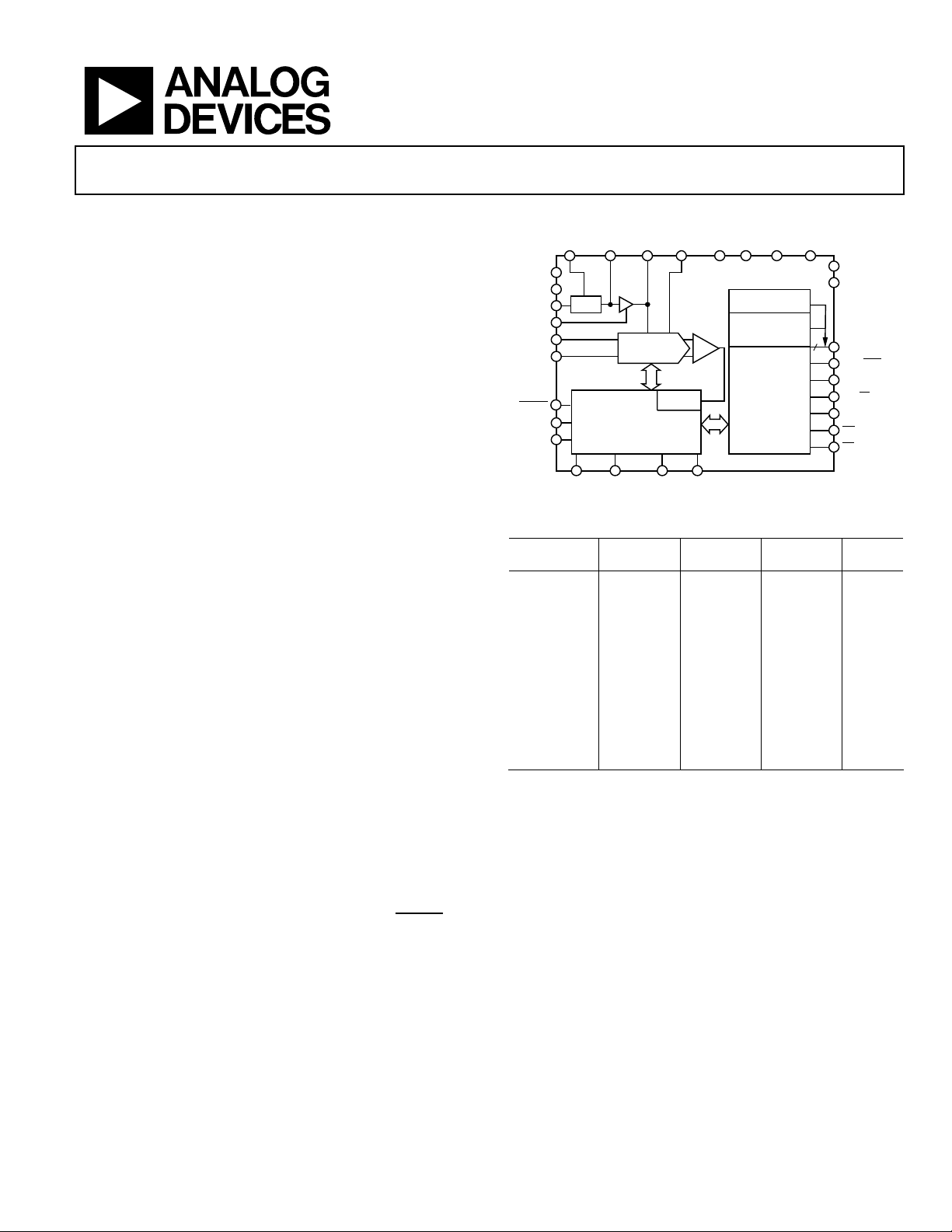
FUNCTIONAL BLOCK DIAGRAM
TEMP
REFBUFIN
AGND
AVDD
PDREF
PDBUF
CNVST
RESET
REF
IN+
IN–
PD
CONTROL L OGIC AND
CALIBRATI ON CIRCUITRY
WARP IMPULSE BI POLAR TEN
REF REFGND
REF
AMP
SWITCHED
CAP DAC
CLOCK
Figure 1.
EE
AD7612
SERIAL DATA
CONFIGURAT ION
PARALLEL
INTERFACE
Table 1. 48-Lead 14-/16-/18-Bit PulSAR Selection
100 kSPS to
Type
Pseudo
Differential
True Bipolar AD7663 AD7665 AD7612
True
Differential
18-Bit, True
Differential
Multichannel/
Simultaneous
250 kSPS
AD7651
AD7660
AD7661
AD7675 AD7676 AD7677 AD7621
AD7678 AD7679 AD7674 AD7641
AD7654
500 kSPS to
570 kSPS
AD7650
AD7652
AD7664
AD7666
AD7655
PRODUCT HIGHLIGHTS
1. Programmable input range and mode selection.
Pins or serial port for selecting input range/mode select.
2. Fast throughput.
In warp mode, the AD7612 is 750 kSPS.
3. Superior Linearity.
No missing 16-bit code. ±1.5 LSB max INL.
4. Internal Reference.
5 V internal reference with a typical drift of ±3 ppm/°C
and an on-chip temperature sensor.
5. Serial or Parallel Interface.
Versatile parallel (16- or 8-bit bus) or 2-wire serial interface
arrangement compatible with 3.3 V or 5 V logic.
DGNDDVDD
OVDD
OGND
PORT
SERIAL
PORT
16
D[15:0]
SER/PAR
BYTESWAP
OB/2C
BUSY
RD
CS
800 kSPS to
1000 kSPS
AD7653
AD7667
AD7671
>1000
kSPS
AD7622
AD7623
AD7643
06265-001
Rev. 0
Information furnished by Analog Devices is believed to be accurate and reliable. However, no
responsibility is assumed by Anal og Devices for its use, nor for any infringements of patents or ot her
rights of third parties that may result from its use. Specifications subject to change without notice. No
license is granted by implication or otherwise under any patent or patent rights of Analog Devices.
Trademarks and registered trademarks are the property of their respective owners.
One Technology Way, P.O. Box 9106, Norwood, MA 02062-9106, U.S.A.
Tel: 781.329.4700 www.analog.com
Fax: 781.461.3113 ©2006 Analog Devices, Inc. All rights reserved.

AD7612
TABLE OF CONTENTS
Features.............................................................................................. 1
Analog Inputs .............................................................................20
Applications....................................................................................... 1
General Description......................................................................... 1
Functional Block Diagram ..............................................................1
Product Highlights........................................................................... 1
Revision History ...............................................................................2
Specifications..................................................................................... 3
Timing Specifications ..................................................................5
Absolute Maximum Ratings............................................................ 7
ESD Caution.................................................................................. 7
Pin Configuration and Function Descriptions............................. 8
Typical Performance Characteristics........................................... 12
Terminology.................................................................................... 16
Theory of Operation ......................................................................17
Overview...................................................................................... 17
Converter Operation.................................................................. 17
Driver Amplifier Choice ........................................................... 21
Voltage Reference Input/Output ..............................................21
Power Supplies............................................................................ 22
Conversion Control................................................................... 23
Interfaces.......................................................................................... 24
Digital Interface.......................................................................... 24
Parallel Interface......................................................................... 24
Serial Interface............................................................................ 25
Master Serial Interface............................................................... 25
Slave Serial Interface.................................................................. 27
Hardware Configuration........................................................... 29
Software Configuration............................................................. 29
Microprocessor Interfacing....................................................... 30
Application Information................................................................ 31
Layout Guidelines....................................................................... 31
Modes of Operation................................................................... 18
Transfer Functions......................................................................18
Typical Connection Diagram ...................................................19
REVISION HISTORY
10/06—Revision 0: Initial Version
Evaluating Performance ............................................................ 31
Outline Dimensions....................................................................... 32
Ordering Guide .......................................................................... 32
Rev. 0 | Page 2 of 32

AD7612
SPECIFICATIONS
AVDD = DVDD = 5 V; OVDD = 2.7 V to 5.5 V; VCC = 15 V; VEE = −15 V; V
Table 2.
Parameter Conditions/Comments Min Typ Max Unit
RESOLUTION 16 Bits
ANALOG INPUT
Voltage Range, VIN V
V
V
V
V
Analog Input CMRR fIN = 100 kHz 75 dB
Input Current V
Input Impedance
THROUGHPUT SPEED
Complete Cycle In warp mode 1.33 s
Throughput Rate In warp mode 1 750
Time Between Conversions In warp mode 1 ms
Complete Cycle In normal mode 1.67 s
Throughput Rate In normal mode 0 600 kSPS
Complete Cycle In impulse mode 2 s
Throughput Rate In impulse mode 0 500 kSPS
DC ACCURACY
Integral Linearity Error
No Missing Codes
Differential Linearity Error
3
3
3
Transition Noise 0.55 LSB
Zero Error (Unipolar or Bipolar) −35 +35 LSB
Zero Error Temperature Drift ±1 ppm/°C
Bipolar Full-Scale Error −50 +50 LSB
Unipolar Full-Scale Error −70 +70 LSB
Full-Scale Error Temperature Drift ±1 ppm/°C
Power Supply Sensitivity AVDD = 5 V ± 5% 3 LSB
AC ACCURACY
Dynamic Range V
V
V
Signal-to-Noise Ratio V
V
Signal-to-(Noise + Distortion) (SINAD) V
V
V
Total Harmonic Distortion fIN = 2 kHz −107 dB
Spurious-Free Dynamic Range fIN = 2 kHz 107 dB
–3 dB Input Bandwidth V
Aperture Delay 2 ns
Aperture Jitter 5 ps rms
Transient Response Full-scale step 500 ns
INTERNAL REFERENCE PDREF = PDBUF = low
Output Voltage REF @ 25°C 4.965 5.000 5.035 V
Temperature Drift –40°C to +85°C ±3 ppm/°C
Line Regulation AVDD = 5 V ± 5% ±15 ppm/V
Long-Term Drift 1000 hours 50 ppm
Turn-On Settling Time C
− V
= 0 V to 5 V −0.1 +5.1 V
IN+
IN−
− V
= 0V to 10 V −0.1 +10.1 V
IN+
IN−
− V
= ±5 V −5.1 +5.1 V
IN+
IN−
− V
= ±10 V −10.1 +10.1 V
IN+
IN−
to AGND −0.1 +0.1 V
IN−
= ±5 V, ±10 V @ 750 kSPS 220
IN
See
Analog Inputs section
−1.5 ±0.75 +1.5 LSB
16 Bits
−1 +1.5 LSB
= 0 V to 5 V, fIN = 2 kHz, −60 dB 92.5 93.5 dB
IN
= 0 V to 10 V, ±5 V, fIN = 2 kHz, −60 dB 94 dB
IN
= ±10 V, fIN = 2 kHz, −60 dB 94.5 dB
IN
= 0 V to 5 V, 0 V to 10 V, fIN = 2 kHz 92 93 dB
IN
= ±5 V, ±10 V, fIN = 2 kHz 94 dB
IN
= ±5 V, fIN = 2 kHz 92.5 dB
IN
= 0 V to 10 V, ±5 V, fIN = 2 kHz 93 dB
IN
= ±10 V, fIN = 2 kHz 93.5 dB
IN
= 0 V to 5 V 45 MHz
IN
= 22 µF 10 ms
REF
= 5 V; all specifications T
REF
to T
MIN
, unless otherwise noted.
MAX
1
µA
2
kSPS
4
5
Rev. 0 | Page 3 of 32

AD7612
Parameter Conditions/Comments Min Typ Max Unit
REFERENCE BUFFER PDREF = high
REFBUFIN Input Voltage Range 2.4 2.5 2.6 V
EXTERNAL REFERENCE PDREF = PDBUF = high
Voltage Range REF 4.75 5 AVDD + 0.1 V
Current Drain 750 kSPS throughput 250 µA
TEMPERATURE PIN
Voltage Output @ 25°C 311 mV
Temperature Sensitivity 1 mV/°C
Output Resistance 4.33 kΩ
DIGITAL INPUTS
Logic Levels
VIL −0.3 +0.6 V
VIH 2.1 OVDD + 0.3 V
IIL −1 +1 µA
IIH −1 +1 µA
DIGITAL OUTPUTS
Data Format Parallel or serial 16-bit
Pipeline Delay
VOL I
VOH I
POWER SUPPLIES
Specified Performance
AVDD 4.75
DVDD 4.75 5 5.25 V
OVDD 2.7 5.25 V
VCC 7 15 15.75 V
VEE −15.75 −15 0 V
Operating Current
AVDD
With Internal Reference 19.5 mA
With Internal Reference Disabled 18 mA
DVDD 6.5 mA
OVDD 0.5 mA
VCC VCC = 15 V, with internal reference buffer 3 mA
VCC = 15 V 2.3 mA
VEE VEE = −15 V 2 mA
Power Dissipation @ 750 kSPS throughput
With Internal Reference PDREF = PDBUF = low 205 230 mW
With Internal Reference Disabled PDREF = PDBUF = high 190 210 mW
In Power-Down Mode10 PD = high 10 µW
TEMPERATURE RANGE
Specified Performance T
1
With VIN = 0 V to 5 V or 0 V to 10 V ranges, the input current is typically 70 A. In all input ranges, the input current scales with throughput. See the Ana log Inp uts section.
2
All specified performance is guaranteed up to 750 kSPS throughout, however throughputs up to 900 kSPS can be used with some linearity performance degradation.
3
Linearity is tested using endpoints, not best fit. All linearity is tested with an external 5 V reference.
4
LSB means least significant bit. All specifications in LSB do not include the error contributed by the reference.
5
All specifications in decibels are referred to a full-scale range input, FSR. Tested with an input signal at 0.5 dB below full-scale, unless otherwise specified.
6
Conversion results are available immediately after completed conversion.
7
4.75 V or V
8
Tested in parallel reading mode.
9
With internal reference, PDREF = PDBUF = low; with internal reference disabled, PDREF = PDBUF = high. With internal reference buffer, PDBUF = low.
10
With all digital inputs forced to OVDD.
11
Consult sales for extended temperature range.
6
8, 9
11
– 0.1 V, whichever is larger.
REF
= 500 µA 0.4 V
SINK
= –500 µA OVDD − 0.6 V
SOURCE
7
5 5.25 V
@ 750 kSPS throughput
to T
MIN
−40 +85 °C
MAX
Rev. 0 | Page 4 of 32
AD7612
TIMING SPECIFICATIONS
AVDD = DVDD = 5 V; OVDD = 2.7 V to 5.5 V; VCC = 15 V; VEE = −15 V; V
Table 3.
Parameter Symbol Min Typ Max Unit
CONVERSION AND RESET (See Figure 33 and Figure 34)
Convert Pulse Width t1 10 ns
Time Between Conversions t2
Warp Mode/Normal Mode/Impulse Mode1 1.33/1.67/2 μs
CNVST Low to BUSY High Delay
BUSY High All Modes (Except Master Serial Read After Convert) t4
Warp Mode/Normal Mode/Impulse Mode 950/1250/1450 ns
Aperture Delay t5 2 ns
End of Conversion to BUSY Low Delay t6 10 ns
Conversion Time t7
Warp Mode/Normal Mode/Impulse Mode 950/1250/1450 ns
Acquisition Time t8
Warp Mode/Normal Mode/Impulse Mode 380 ns
RESET Pulse Width t9 10 ns
PARALLEL INTERFACE MODES (See Figure 35 and Figure 37)
CNVST Low to DATA Valid Delay
Warp Mode/Normal Mode/Impulse Mode 910/1160/1410 ns
DATA Valid to BUSY Low Delay t11 20 ns
Bus Access Request to DATA Valid t12 40 ns
Bus Relinquish Time t13 2 15 ns
MASTER SERIAL INTERFACE MODES2 (See Figure 39 and Figure 40)
CS Low to SYNC Valid Delay
CS Low to Internal SDCLK Valid Delay2
CS Low to SDOUT Delay
CNVST Low to SYNC Delay, Read During Convert
Warp Mode/Normal Mode/Impulse Mode 65/315/560 ns
SYNC Asserted to SDCLK First Edge Delay t18 3 ns
Internal SDCLK Period3 t
Internal SDCLK High3 t
Internal SDCLK Low3 t
SDOUT Valid Setup Time3 t
SDOUT Valid Hold Time3 t
SDCLK Last Edge to SYNC Delay3 t
CS High to SYNC HI-Z
CS High to Internal SDCLK HI-Z
CS High to SDOUT HI-Z
BUSY High in Master Serial Read After Convert3 t
CNVST Low to SYNC Delay, Read After Convert
Warp Mode/Normal Mode/Impulse Mode t29 830/1070/1310 ns
SYNC Deasserted to BUSY Low Delay t30 25 ns
= 5 V; all specifications T
REF
t
35 ns
3
t
10
t
10 ns
14
t
10 ns
15
t
10 ns
16
t
17
30 45 ns
19
15 ns
20
10 ns
21
4 ns
22
5 ns
23
5 ns
24
t
10 ns
25
t
10 ns
26
t
10 ns
27
See Table 4
28
MIN
to T
, unless otherwise noted.
MAX
Rev. 0 | Page 5 of 32
AD7612
Parameter Symbol Min Typ Max Unit
SLAVE SERIAL/SERIAL CONFIGURATION INTERFACE MODES2 (See Figure 42,
Figure 43, and Figure 45)
External SDCLK, SCCLK Setup Time t31 5 ns
External SDCLK Active Edge to SDOUT Delay t32 2 18 ns
SDIN/SCIN Setup Time t33 5 ns
SDIN/SCIN Hold Time t34 5 ns
External SDCLK/SCCLK Period t35 25 ns
External SDCLK/SCCLK High t36 10 ns
External SDCLK/SCCLK Low t37 10 ns
1
In warp mode only, the time between conversions is 1 ms; otherwise, there is no required maximum time.
2
In serial interface modes, the SDSYNC, SDSCLK, and SDOUT timings are defined with a maximum load CL of 10 pF; otherwise, the load is 60 pF maximum.
3
In serial master read during convert mode. See Table 4 for serial master read after convert mode.
Table 4. Serial Clock Timings in Master Read After Convert Mode
DIVSCLK[1]
DIVSCLK[0] Symbol 0 1 0 1 Unit
SYNC to SDCLK First Edge Delay Minimum t18 3 20 20 20 ns
Internal SDCLK Period Minimum t19 30 60 120 240 ns
Internal SDCLK Period Maximum t19 45 90 180 360 ns
Internal SDCLK High Minimum t20 15 30 60 120 ns
Internal SDCLK Low Minimum t21 10 25 55 115 ns
SDOUT Valid Setup Time Minimum t22 4 20 20 20 ns
SDOUT Valid Hold Time Minimum t23 5 8 35 90 ns
SDCLK Last Edge to SYNC Delay Minimum t24 5 7 35 90 ns
BUSY High Width Maximum t28
Warp Mode 1.65 2.35 3.75 6.53 μs
Normal Mode 1.9 2.6 4.00 6.78 μs
Impulse Mode 2.15 2.85 4.25 7.03 μs
0 0 1 1
1.6mA I
TO OUTPUT
PIN
C
L
60pF
500µA I
NOTES
1. IN SERIAL INTERFACE MODES, THE S Y NC, SCLK, AND
SDOUT ARE DEF INED WITH A M AXIMUM LOAD
OF 10pF; OTHERWISE, THE LOAD IS 60pF MAXIMUM.
C
L
OL
1.4V
OH
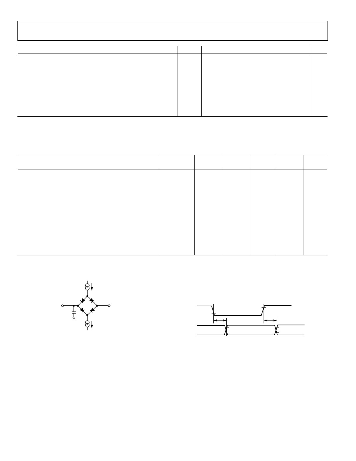
Figure 2. Load Circuit for Digital Interface Timing,
SDOUT, SYNC, and SCLK Outputs, C
= 10 pF
L
6265-002
Rev. 0 | Page 6 of 32
2V
0.8V
t
DELAY
2V
t
DELAY
2V
0.8V0.8V
06265-003
Figure 3. Voltage Reference Levels for Timing
AD7612
ABSOLUTE MAXIMUM RATINGS
Table 5.
Parameter Rating
Analog Inputs/Outputs
IN+1, IN−1 to AGND VEE − 0.3 V to VCC + 0.3 V
REF, REFBUFIN, TEMP,
REFGND to AGND
AVDD + 0.3 V to
AGND − 0.3 V
Ground Voltage Differences
AGND, DGND, OGND ±0.3 V
Supply Voltages
AVDD, DVDD, OVDD −0.3 V to +7 V
AVDD to DVDD, AVDD to OVDD ±7 V
DVDD to OVDD ±7 V
VCC to AGND, DGND –0.3 V to +16.5
VEE to GND +0.3 V to −16.5
Digital Inputs −0.3 V to OVDD + 0 .3 V
PDREF, PDBUF
2
±20 mA
Internal Power Dissipation3 700 mW
Internal Power Dissipation4 2.5 W
Junction Temperature 125°C
Storage Temperature Range −65°C to +125°C
1
See the Analog Inputs section.
2
See the Voltage Reference Input section.
3
Specification is for the device in free air: 48-Lead LFQP; θJA = 91°C/W,
θJC = 30°C/W.
4
Specification is for the device in free air: 48-Lead LFCSP; θJA = 26°C/W.
Stresses above those listed under Absolute Maximum Ratings
may cause permanent damage to the device. This is a stress
rating only; functional operation of the device at these or any
other conditions above those indicated in the operational
section of this specification is not implied. Exposure to absolute
maximum rating conditions for extended periods may affect
device reliability.
ESD CAUTION
Rev. 0 | Page 7 of 32
AD7612
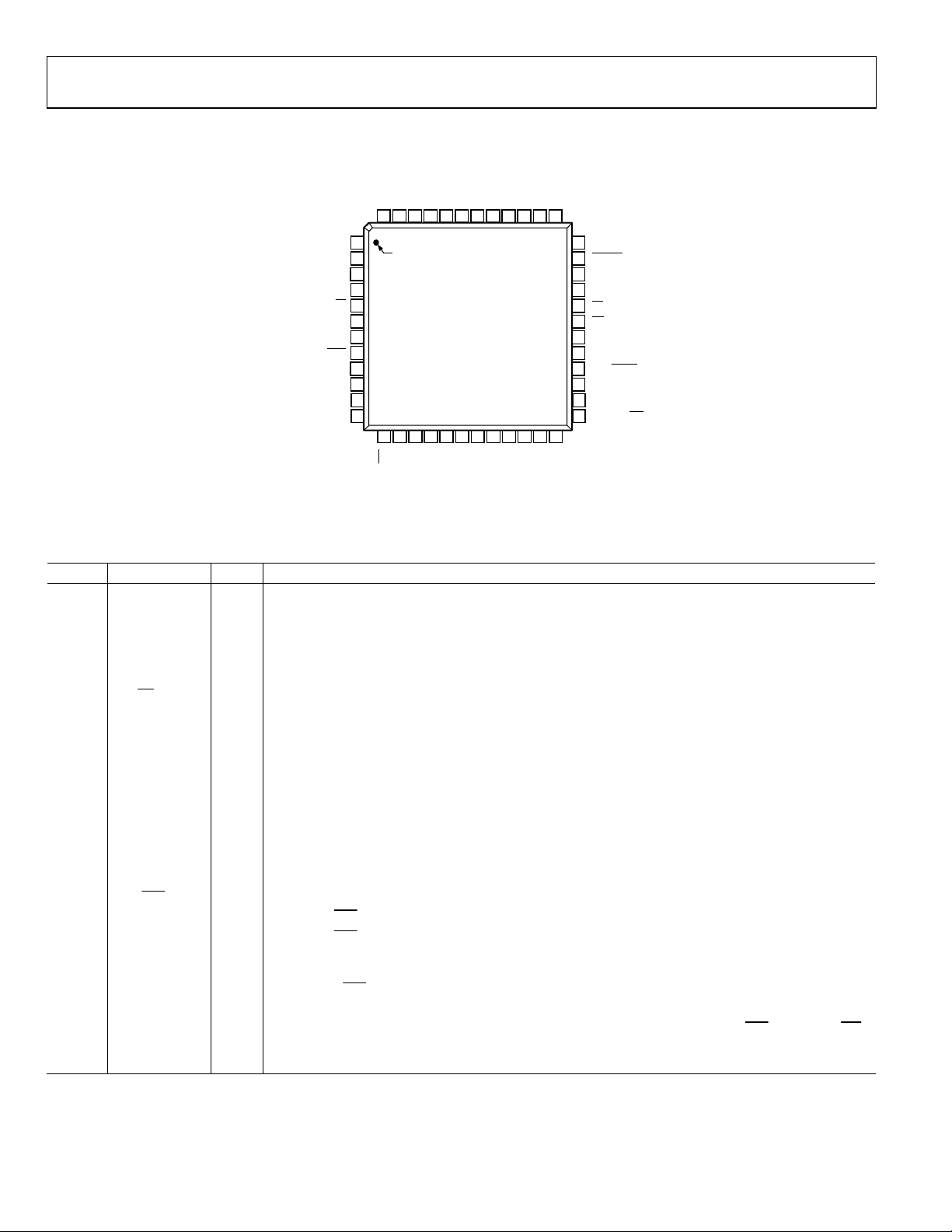
PIN CONFIGURATION AND FUNCTION DESCRIPTIONS
VEE
DGND
IN–
VCC
REFGND
REF
36
BIPOLAR
35
CNVST
34
PD
33
RESET
32
CS
31
RD
30
TEN
29
BUSY
28
D15/SCCS
27
D14/SCCLK
26
D13/SCIN
25
D12/HW/SW
D10/SYNC
D8/SDOUT
D9/SDCLK
06265-004
D11/RDERROR
AGND
AVDD
AGND
BYTESWAP
OB/2C
WARP
IMPULSE
SER/PAR
D0
D1
D2/DIVSCLK[0]
D3/DIVSCLK[1]
PDBUF
PDREF
REFBUFIN
48 47 46 45 44 43 42 41 40 39 38 37
1
PIN 1
2
3
4
5
6
7
8
9
10
11
12
13
14 15 16 17 18 19 20 21 22 23 24
D4/EXT/INT
D6/INVSCLK
D5/INVSYNC
IN+
TEMP
AVDD
AD7612
TOP VIEW
(Not to Scale)
OVDD
OGND
D7/RDC/SDIN
AGND
DVDD
Figure 4. Pin Configuration
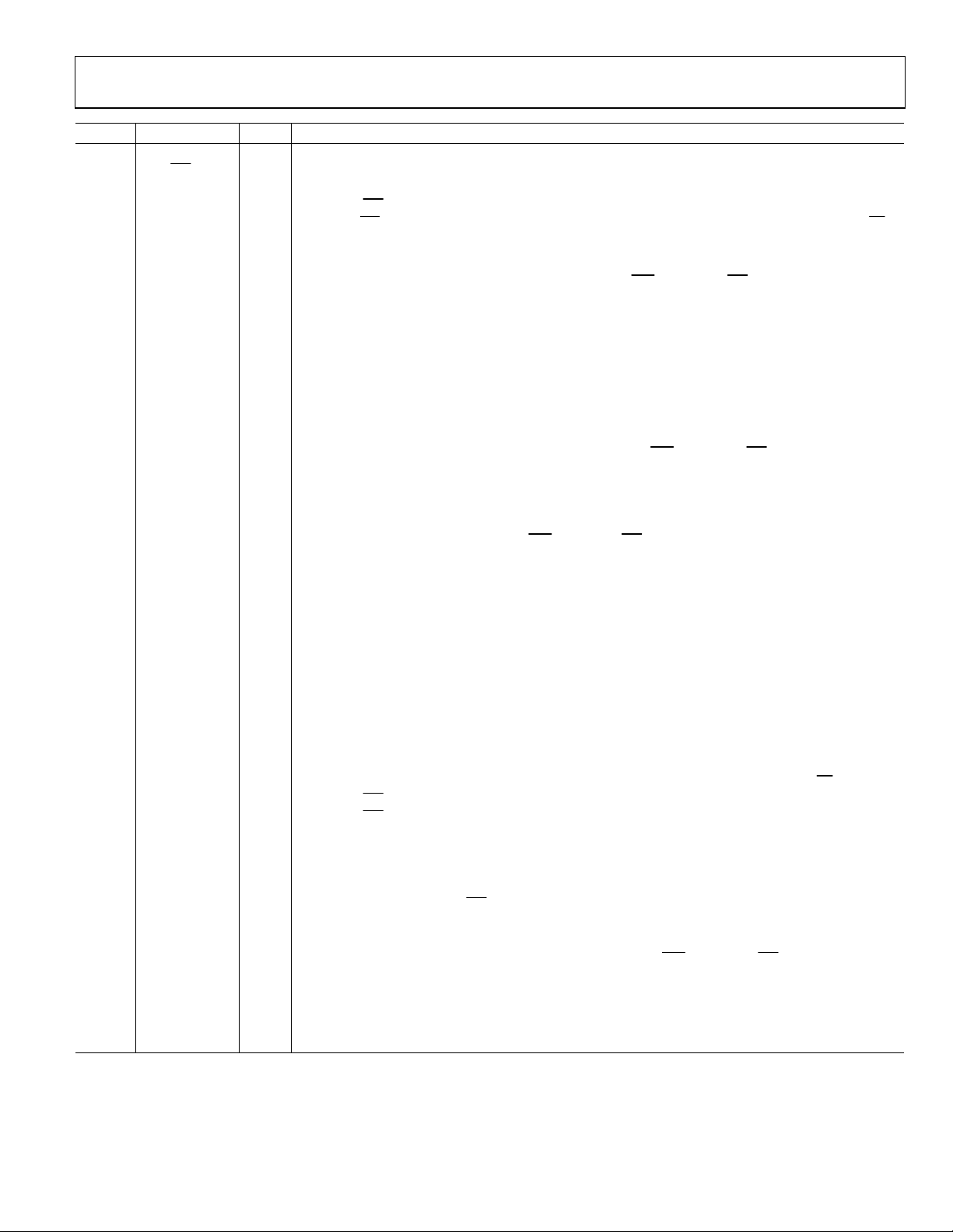
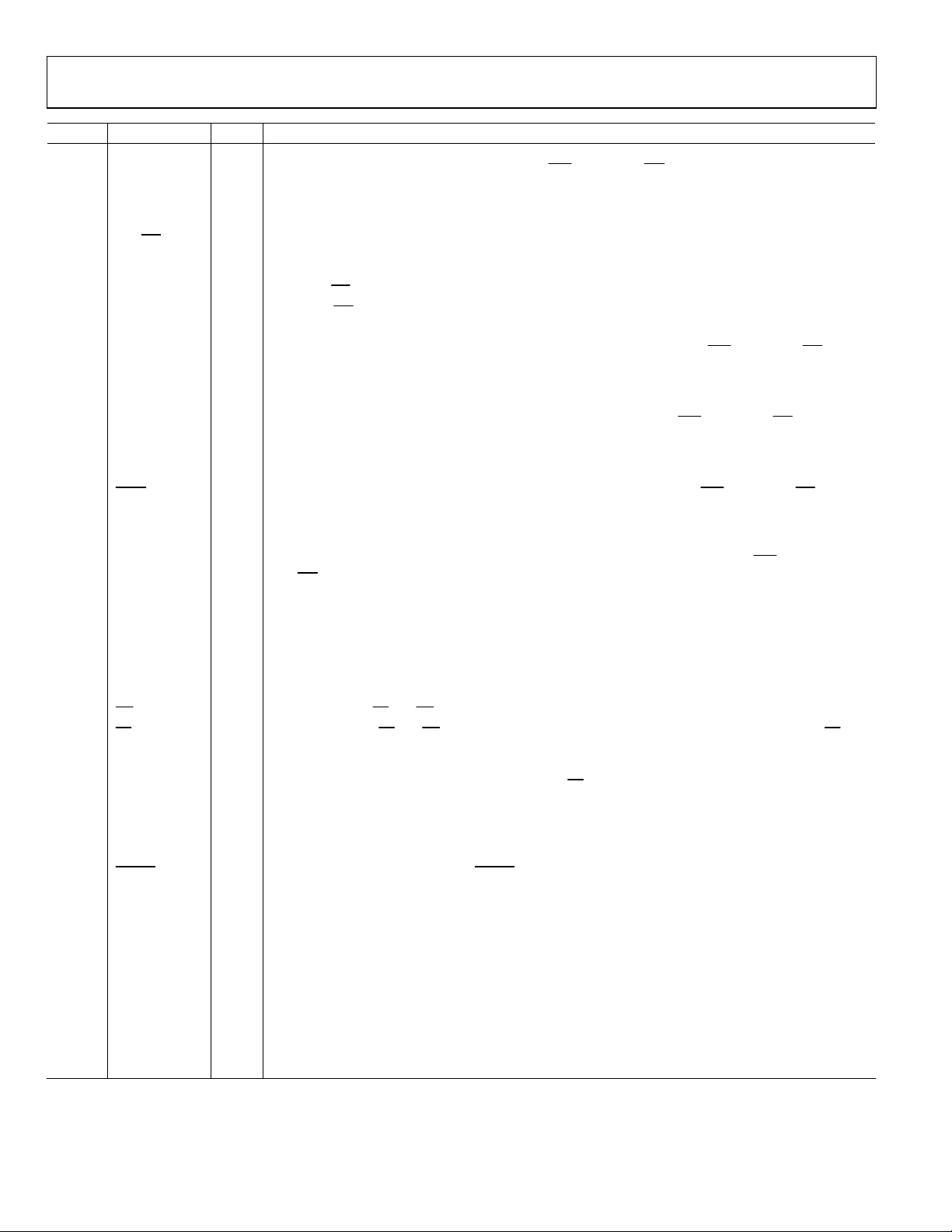
Table 6. Pin Function Descriptions
Pin No. Mnemonic Type1 Description
1, 3, 42 AGND P
Analog Power Ground Pins. Ground reference point for all analog I/O. All analog I/O should be
referenced to AGND and should be connected to the analog ground plane of the system. In addition,
the AGND, DGND, and OGND voltages should be at the same potential.
2, 44 AVDD P Analog Power Pins. Nominally 4.75 V to 5.25 V and decoupled with 10 μF and 100 nF capacitors.
4 BYTESWAP DI
Parallel Mode Selection (8-Bit/16-Bit). When high, the LSB is output on D[15:8] and the MSB is output
on D[7:0]; when low, the LSB is output on D[7:0] and the MSB is output on D[15:8].
2
5
OB/2C
DI
Straight Binary/Binary Twos Complement Output. When high, the digital output is straight binary.
When low, the MSB is inverted resulting in a twos complement output from its internal shift register.
6 WARP DI2 Conversion Mode Selection. Used in conjunction with the IMPULSE input per the following:
Conversion Mode WARP IMPULSE
Normal Low Low
Impulse Low High
Warp High Low
Normal High High
See the Modes of Operation section for a more detailed description.
7 IMPULSE DI2
Conversion Mode Selection. See the WARP pin description in the previous row of this table. See the
Modes of Operation section for a more detailed description.
8
SER/PAR
DI Serial/Parallel Selection Input.
When SER/PAR
When SER/PAR
= low, the parallel mode is selected.
= high, the serial modes are selected. Some bits of the data bus are used as a serial port
and the remaining data bits are high impedance outputs.
9, 10 D[0:1] DO
Bit 0 and Bit 1 of the parallel port data output bus. These pins are always outputs regardless of the
state of SER/PAR
.
11, 12 D[2:3] or DI/O In parallel mode, these outputs are used as Bit 2 and Bit 3 of the parallel port data output bus.
DIVSCLK[0:1]
Serial Data Division Clock Selection. In serial master read after convert mode (SER/PAR
= high, EXT/INT
= low, RDC/SDIN = low) these inputs can be used to slow down the internally generated serial data
clock that clocks the data output. In other serial modes, these pins are high impedance outputs.
Rev. 0 | Page 8 of 32
AD7612
Pin No. Mnemonic Type1 Description
13 D4 or DI/O In parallel mode, this output is used as Bit 4 of the parallel port data output bus.
14 D5 or DI/O In parallel mode, this output is used as Bit 5 of the parallel port data output bus.
INVSYNC
15 D6 or DI/O In parallel mode, this output is used as Bit 6 of the parallel port data output bus.
INVSCLK In all serial modes, invert SDCLK/SCCLK select. This input is used to invert both SDCLK and SCCLK.
16 D7 or DI/O In parallel mode, this output is used as Bit 7 of the parallel port data output bus.
RDC or
SDIN
17 OGND P
18 OVDD P
19 DVDD P
20 DGND P
21 D8 or DO In parallel mode, this output is used as Bit 8 of the parallel port data output bus.
SDOUT
22 D9 or DI/O In parallel mode, this output is used as Bit 9 of the parallel port data output bus.
SDCLK
23 D10 or DO In parallel mode, this output is used as Bit 10 of the parallel port data output bus.
SYNC
EXT/INT
Serial Data Clock Source Select. In serial mode, this input is used to select the internally generated
(master) or external (slave) serial data clock for the AD7612 output data.
When EXT/INT
When EXT/INT = high, slave mode; the output data is synchronized to an external clock signal (gated by CS)
connected to the SDCLK input.
Serial Data Invert Sync Select. In serial master mode (SER/PAR
to select the active state of the SYNC signal.
When INVSYNC = low, SYNC is active high.
When INVSYNC = high, SYNC is active low.
When INVSCLK = low, the rising edge of SDCLK/SCCLK are used.
When INVSCLK = high, the falling edge of SDCLK/SCCLK are used.
Serial Data Read During Convert. In serial master mode (SER/PAR
select the read mode. Refer to the Master Serial Interface section.
When RDC = low, the current result is read after conversion. Note the maximum throughput is not
attainable in this mode.
When RDC = high, the previous conversion result is read during the current conversion.
Serial Data In. In serial slave mode (SER/PAR
daisy-chain the conversion results from two or more ADCs onto a single SDOUT line. The digital data
level on SDIN is output on SDOUT with a delay of 16 SDCLK periods after the initiation of the read sequence.
Input/Output Interface Digital Power Ground. Ground reference point for digital outputs. Should be
connected to the system digital ground ideally at the same potential as AGND and DGND.
Input/Output Interface Digital Power. Nominally at the same supply as the supply of the host interface
2.5 V, 3 V, or 5 V and decoupled with 10 μF and 100 nF capacitors.
Digital Power. Nominally at 4.75 V to 5.25 V and decoupled with 10 μF and 100 nF capacitors. Can be
supplied from AVDD.
Digital Power Ground. Ground reference point for digital outputs. Should be connected to system
digital ground ideally at the same potential as AGND and OGND.
Serial Data output. In all serial modes this pin is used as the serial data output synchronized to SDCLK.
Conversion results are stored in an on-chip register. The AD7612 provides the conversion result, MSB
first, from its internal shift register. The data format is determined by the logic level of OB/2C
When EXT/INT
When EXT/INT = high, (slave mode).
When INVSCLK = low, SDOUT is updated on SDCLK rising edge.
When INVSCLK = high, SDOUT is updated on SDCLK falling edge.
Serial Data Clock. In all serial modes, this pin is used as the serial data clock input or output, dependent
on the logic state of the EXT/INT
the logic state of the INVSCLK pin.
Serial Data Frame Synchronization. In serial master mode (SER/PAR
is used as a digital output frame synchronization for use with the internal data clock.
When a read sequence is initiated and INVSYNC = low, SYNC is driven high and remains high while the
SDOUT output is valid.
When a read sequence is initiated and INVSYNC = high, SYNC is driven low and remains low while the
SDOUT output is valid.
= low, master mode; the internal serial data clock is selected on SDCLK output.
= high, EXT/INT = low). This input is used
= high, EXT/INT = low) RDC is used to
= high EXT/INT = high) SDIN can be used as a data input to
.
= low, (master mode) SDOUT is valid on both edges of SDCLK.
pin. The active edge where the data SDOUT is updated depends on
= high, EXT/INT= low), this output
Rev. 0 | Page 9 of 32
AD7612
Pin No. Mnemonic Type1 Description
24 D11 or DO In parallel mode, this output is used as Bit 11 of the parallel port data output bus.
RDERROR
25 D12 or DI/O In parallel mode, this output is used as Bit 12 of the parallel port data output bus.
26 D13 or DI/O In parallel mode, this output is used as Bit 13 of the parallel port data output bus.
SCIN
27 D14 or DI/O In parallel mode, this output is used as Bit 14 of the parallel port data output bus.
SCCLK
28 D15 or DI/O In parallel mode, this output is used as Bit 15 of the parallel port data output bus.
29 BUSY DO
30 TEN DI2 Input Range Select. Used in conjunction with BIPOLAR per the following:
31
32
33 RESET DI
34 PD DI2
35
36 BIPOLAR DI2 Input Range Select. See description for Pin 30.
37 REF AI/O
38 REFGND AI Reference Input Analog Ground. Connected to analog ground plane.
39 IN− AI Analog Input Ground Sense. Should be connected to the analog ground plane or to a remote sense ground.
40 VCC P High Voltage Positive Supply. Normally +7 V to +15 V.
41 VEE P High Voltage Negative Supply. Normally 0 V to −15 V (0 V in unipolar ranges).
HW/SW
SCCS
RD
CS
CNVST
DI
DI
DI
Serial Data Read Error. In serial slave mode (SER/PAR
incomplete data read error flag. If a data read is started and not completed when the current
conversion is complete, the current data is lost and RDERROR is pulsed high.
Serial Configuration Hardware/Software Select. In serial mode, this input is used to configure
the AD7612 by hardware or software. See the Hardware Configuration section and Software
Configuration section.
When HW/SW
When HW/SW
Serial Configuration Data Input. In serial software configuration mode (SER/PAR
this input is used to serially write in, MSB first, the configuration data into the serial configuration
register. The data on this input is latched with SCCLK. See the Software Configuration section.
Serial Configuration Clock. In serial software configuration mode (SER/PAR
input is used to clock in the data on SCIN. The active edge where the data SCIN is updated depends on
the logic state of the INVSCLK pin. See the Software Configuration section.
Serial Configuration Chip Select. In serial software configuration mode (SER/PAR = high, HW/SW = low)
this input enables the serial configuration port. See the Software Configuration section.
Busy Output. Transitions high when a conversion is started, and remains high until the conversion
is complete and the data is latched into the on-chip shift register. The falling edge of BUSY can be
used as a data ready clock signal. Note that in master read after convert mode (SER/PAR
EXT/INT = low, RDC = low) the busy time changes according to Table 4.
Input Range BIPOLAR TEN
0 V to 5 V Low Low
0 V to 10 V Low High
±5 V High Low
±10 V High High
Read Data. When CS and RD are both low, the interface parallel or serial output bus is enabled.
Chip Select. When CS and RD are both low, the interface parallel or serial output bus is enabled. CS is
also used to gate the external clock in slave serial mode (not used for serial programmable port).
Reset Input. When high, reset the AD7612. Current conversion, if any, is aborted. The falling edge of
RESET resets the data outputs to all zero’s (with OB/2C
See the Digital Interface section. If not used, this pin can be tied to OGND.
Power-Down Input. When PD = high, power down the ADC. Power consumption is reduced and
conversions are inhibited after the current one is completed. The digital interface remains active
during power down.
Conversion Start. A falling edge on CNVST puts the internal sample-and-hold into the hold state and
initiates a conversion.
Reference Input/Output.
When PDREF/PDBUF = low, the internal reference and buffer are enabled, producing 5 V on this pin.
When PDREF/PDBUF = high, the internal reference and buffer are disabled, allowing an externally
supplied voltage reference up to AVDD volts. Decoupling with at least a 22 μF is required with or
without the internal reference and buffer. See the Reference Decoupling section.
= low, the AD7612 is configured through software using the serial configuration register.
= high, the AD7612 is configured through dedicated hardware input pins.
= high, EXT/INT = high), this output is used as an
= high, HW/SW = low)
= high, HW/SW = low) this
= high,
= high) and clears the configuration register.
Rev. 0 | Page 10 of 32
 Loading...