Analog Devices AD760AQ Datasheet

16/18-Bit Self-Calibrating
+10V
REF
10k
S
OUT
SPAN/
BIP
OFF
V
OUT
9.95k
LDAC
REF IN
REF OUT
HBE
SER
CLR
10k
AD760
UNI/
BIP CLR
OR LBE
MUX
OUT
MUX
IN
AGND
S
IN
OR
DB0 DB2 DB7CS
MSB/
LSB
OR
DB1
12
18/16
SERIAL
OR
24
23
15
27
28
22
25
17
18
20
21
19
MAIN DAC
CONTROL
LOGIC
16
26
RAM
CALIBRATION SEQUENCER
CALOK –V
EE+VCC+VLL
DGND
CAL
1
2 3 5
6
4
14
16/18-BIT
INPUT REGISTER
13 7
CALIBRATION DAC
16/18-BIT DAC LATCH
a
FEATURES
±0.2 LSB (±0.00031%) Typ Peak DNL and INL
±0.5 LSB (±0.00076%) Typ Unipolar Offset, Bipolar Zero
17-Bit Monotonicity Guaranteed
18-Bit Resolution (in Serial Mode)
Complete 16/18-Bit D/A Function
On-Chip Output Amplifier
On-Chip Buried Zener Voltage Reference
Microprocessor Compatible
Serial or Byte Input
Double Buffered Latches
Asynchronous Clear Function
Serial Output Pin Facilitates Daisy Chaining
Pin Strappable Unipolar or Bipolar Output
Low THD+N: 0.005%
MUX Output Control on Power-Up and Supply Glitches
PRODUCT DESCRIPTION
The AD760 is a complete 16/18-bit self-calibrating monolithic
DAC (DACPORT®) with onboard voltage reference, double
buffered latches and output amplifier. It is manufactured on
Analog Devices’ BiMOS II process. This process allows the fabrication of low power CMOS logic functions on the same chip
as high precision bipolar linear circuitry.
Self-calibration is initiated by simply pulsing the
The CALOK pin indicates when calibration has been successfully completed. The output multiplexer (MUX
to send the output to the bottom of the output range during
calibration.
Data can be loaded into the AD760 as straight binary, serial
data or as two 8-bit bytes. In serial mode, 16-bit or 18-bit data
can be used and the serial mode input format is pin selectable,
to be MSB or LSB first. This is made possible by three digital
input pins which have dual functions (Pins 12, 13, and 14). In
byte mode the user can similarly define whether the high byte or
low byte is loaded first. The serial output (S
user to daisy chain several AD760s by shifting the data through
the input latch into the next DAC thus minimizing the number
of control lines required in a multiple DAC application. The
double buffered latch structure eliminates data skew errors and
provides for simultaneous updating of DACs in a multi-DAC
system.
The asynchronous
output to minus full-scale or midscale depending on the state of
Pin 17 when
REV. A
Information furnished by Analog Devices is believed to be accurate and
reliable. However, no responsibility is assumed by Analog Devices for its
use, nor for any infringements of patents or other rights of third parties
which may result from its use. No license is granted by implication or
otherwise under any patent or patent rights of Analog Devices.
CLR is strobed. The AD760 also powers up with the
CLR function can be configured to clear the
CAL pin low.
) can be used
OUT
) pin allows the
OUT
Serial/Byte DACPORT
AD760
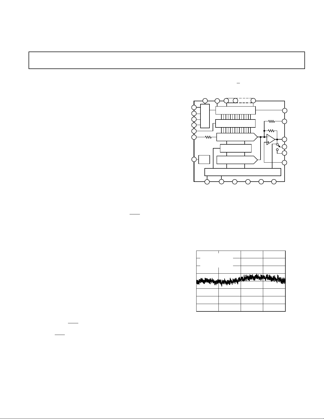
FUNCTIONAL BLOCK DIAGRAM
MUX output in a predetermined state by means of a digital and
analog power supply detection circuit. This is particularly useful for robotic and industrial control applications.
The AD760 is available in a 28-pin, 600 mil cerdip package.
The AQ version is specified from –40°C to +85°C.
V
= –10V TO +10V
OUT
0.75
RL = 2kΩ
CL = 1000pF
0.25
0
–0.25
RELATIVE ACCURACY – LSB
–0.75
0 16384 32768 49152 65535
Typical Integral Nonlinearity
DACPORT is a registered trademark of Analog Devices, Inc.
One Technology Way, P.O. Box 9106, Norwood. MA 02062-9106, U.S.A.
Tel: 617/329-4700 Fax: 617/326-8703
INPUT CODE – Decimal
© Analog Devices, Inc., 1995

AD760–SPECIFICATIONS
(@ TA = +25°C, VCC = +15 V, VEE = –15 V, VLL = + 5 V, unless otherwise noted)
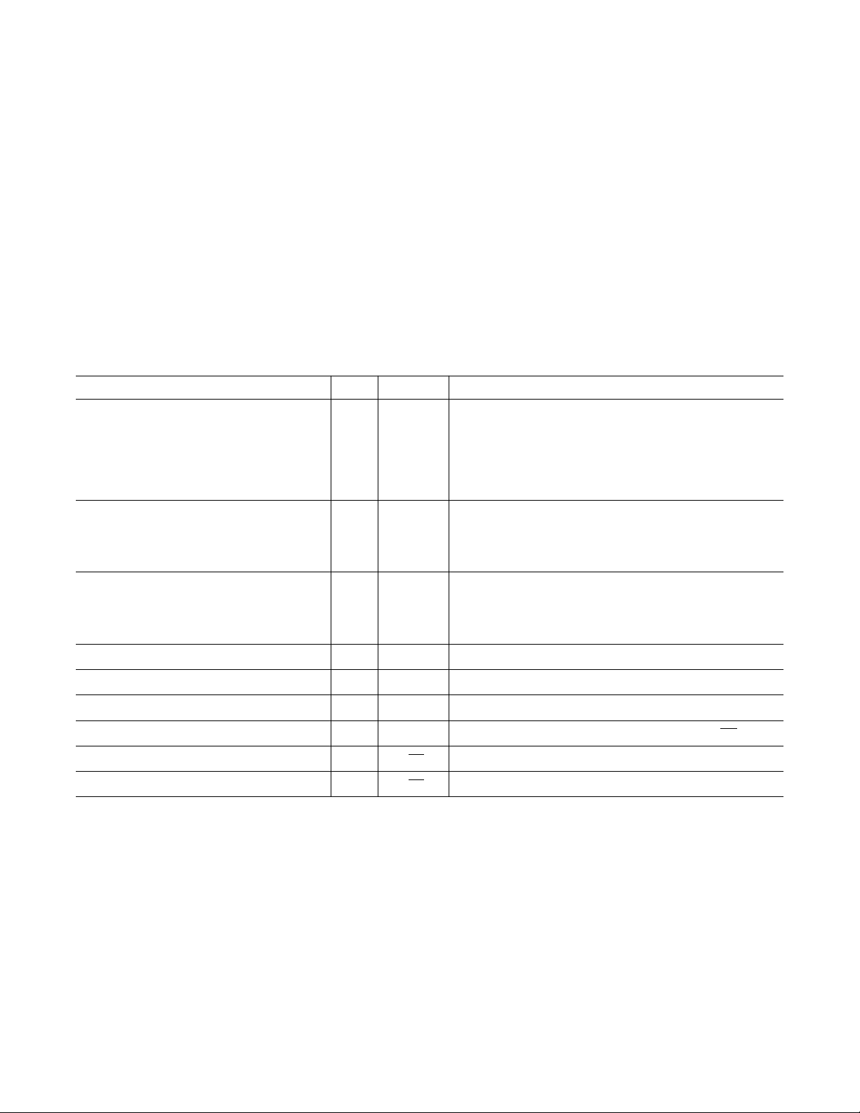
Model Min Typ Max Units
AD760AQ
RESOLUTION
TRANSFER FUNCTION CHARACTERISTICS
With Calibration @ T
1
3
; –40°C T
CAL
CAL
2
+85°C
16/18 Bits
Integral Nonlinearity ±0.2 ±0.75 16-Bit LSB
Differential Nonlinearity ±0.2 ±0.5 16-Bit LSB
Monotonicity 17 18 Bits
Unipolar Offset ±0.5 ±1 16-Bit LSB
Bipolar Zero Error ±0.5 ±1 16-Bit LSB
Without Calibration
Integral Nonlinearity ±2 16-Bit LSB
T
MIN
to T
MAX
±4 16-Bit LSB
Integral Nonlinearity Drift 0.015 16-Bit LSB/°C
Differential Nonlinearity ±2 16-Bit LSB
T
MIN
to T
MAX
±4 16-Bit LSB
Differential Nonlinearity Drift 0.015 16-Bit LSB/°C
Monotonicity Over Temperature 14 Bits
Unipolar Offset ±2.5 mV
Unipolar Offset Drift (T
MIN
to T
) 3 ppm/°C
MAX
Bipolar Zero Error ±10 mV
Bipolar Zero Error Drift (T
Gain Error
Gain Drift
DAC Gain Error
DAC Gain Drift6 (T
4, 5
5
(T
MIN
to T
6
MIN
MIN
to T
) 5 ppm/°C
MAX
±0.10 % of FSR
) 25 ppm/°C
MAX
±0.05 % of FSR
to T
) 10 ppm/°C
MAX
INPUT RESISTANCE
REFIN 7 10 13 k
SPAN/BIP OFF 7 10 13 k
REFERENCE OUTPUT
Voltage 9.99 10.00 10.01 V
Drift 25 ppm/°C
External Current
7
24 mA
Capacitive Load 1000 pF
Short Circuit Current 25 mA
Long-Term Stability 50 ppm/1000 Hrs
OUTPUT CHARACTERISTICS
2
Output Voltage Range
Unipolar Configuration 0 +10 V
Bipolar Configuration –10 +10 V
Output Current 5 mA
Capacitive Load 1000 pF
Short Circuit Current 25 mA
MUX
DIGITAL INPUTS (T
V
V
I
Resistance 0.9 7 k
OUT
to T
(Logic “1”) 2.0 V
IH
(Logic “0”) 0 0.8 V
IL
(VIH = VLL) ±10 µA
IH
MIN
MAX
)
LL
V
IIL (VIL = 0 V) ±10 µA
to T
DIGITAL OUTPUT (T
(IOH = –0.6 mA) 2.4 V
V
OH
MIN
MAX
)
VOL (IOL = 1.6 mA) 0.4 V
POWER SUPPLIES
Voltage
8
V
CC
8
V
EE
V
LL
+14.25 +15.75 V
–15.75 –14.25 V
+4.75 +5.25 V
Current (No Load)
I
CC
I
EE
I
LL
–21 –18 mA
+18 +21 mA
@ VIH, VIL = 5.0 V, 0 V 2 3 mA
@ V
, VIL = 2.4 V, 0.4 V 3 7.5 mA
Power Supply Sensitivity with V
IH
= 10 V 1 ppm/%
OUT
Power Dissipation (Static, No Load) 600 725 mW
TEMPERATURE RANGE
Specified Performance (A) –40 +85 °C
–2–
REV. A

AD760
NOTES
1
For 18-bit resolution, 1 LSB = 0.00038% of FSR. For 16-bit resolution, 1 LSB = 0.0015% of FSR. For 14-bit resolution, 1 LSB = 0.006% of FSR. FSR stands for
full-scale range and is 10 V in unipolar mode and 20 V in bipolar mode.
2
Characteristics are guaranteed at V
3
T
is the calibration temperature.
CAL
4
Gain Error is measured with a fixed 50 resistor as shown in Figure 5a and Figure 6a.
5
Gain Error and gain drift are measured with the internal reference. The internal reference is the main contributor to the gain drift. If lower drift is required, the
AD760 can be used with a precision external reference such as the AD587, AD586 or AD688.
6
DAC Gain Error is measured without the on-chip voltage reference. It represents the performance that can be obtained with an external precision reference.
7
External current is defined as the current available in addition to that supplied to REF IN and SPAN/BIPOLAR OFFSET on the AD760.
8
Operation on ±12 V supplies is possible using an external reference such as the AD586 and reducing the output range. Refer to the Internal/External Reference
section.
Specifications subject to change without notice.
Pin (23).
OUT
AC PERFORMANCE CHARACTERISTICS
Ratio, these characteristics are included for design guidance only and are not subject to test. THD+N and SNR are 100% tested. (T
< T
, VCC = +15 V, VEE = –15 V, VLL = +5 V, tested at V
MAX
With the exception of Total Harmonic Distortion + Noise and Signal-to-Noise
except where noted.)
OUT
MIN
Parameter Limit Units Test Conditions/Comments
Output Settling Time 13 µs max 20 V Step, T
(Time to +0.0008% FS, with 8 µs typ 20 V Step, T
= +25°C
A
= +25°C
A
2 k , 1000 pF Load) 10 µs typ 20 V Step
6 µs typ 10 V Step, TA = +25°C
8 µs typ 10 V Step
2.5 µs typ 1 LSB Step
MUX
Recovery Time Recovery time is referenced to the rising edge of CALOK,
OUT
(Time to +0.0008% FS, with when MUX
100 pF Load) MUX
IN
2 µs typ MUXIN, V
switches from MUXIN to V
OUT
= V
prior to calibration.
OUT
= –10 V to +10 V
OUT
OUT
.
Total Harmonic Distortion + Noise
A, S Grade 0.005 % max 0 dB, 1001 Hz. Sample Rate = 100 kHz. TA = +25°C
A, S Grade 0.03 % max –20 dB, 1001 Hz. Sample Rate = 100 kHz. T
= +25°C
A
A, S Grade 3.0 % max –60 dB, 1001 Hz. Sample Rate = 100 kHz. TA = +25°C
Signal-to-Noise Ratio 94 dB min TA = +25°C, byte load
Digital-to-Analog Glitch Impulse 15 nV-s typ DAC alternately loaded with 8000H and 7FFF
MUX
Glitch Impulse 30 nV-s typ 100 pF Load. MUXIN = V
OUT
= negative full scale
OUT
H
Digital Feedthrough 2 nV-s typ DAC alternately loaded with 0000H and FFFFH. CS high
< T
A
Output Noise Voltage Density (1 kHz–1 MHz) 120 nV/ Hz typ Measured at V
, 20 V span, excludes internal reference
OUT
Reference Noise (1 kHz–1 MHz) 125 nV/ Hz typ Measured at REF OUT
Specifications are subject to change without notice.
REV. A
–3–

AD760
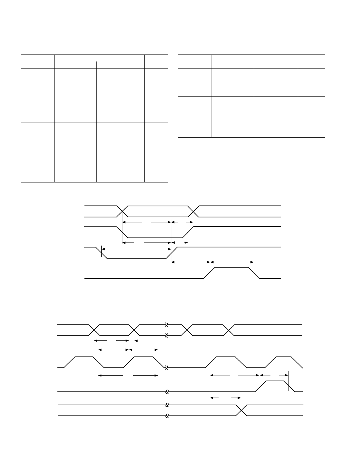
TIMING CHARACTERISTICS
Limit
Parameter +25°C T
(Figure 1a)
t
CS
t
DS
t
DH
t
BES
t
BEH
t
LH
t
LW
50 60 ns min
50 60 ns min
0 10 ns min
50 60 ns min
0 10 ns min
200 350 ns min
50 50 ns min
(Figure 1b)
t
CLK
t
LO
t
HI
t
DS
t
DH
t
LH
t
LW
t
PROP
80 100 ns min
40 50 ns min
40 50 ns min
50 60 ns min
0 10 ns min
200 350 ns min
50 50 ns min
70 100 ns max
DB0–7
HBE OR
LBE
CS
MIN
(VCC = +15 V, VEE = –15 V, VLL = +5 V, VIH = 2.4 V, VIL = 0.4 V)
Limit
to T
MAX
Units
Parameter +25°C T
(Figure 1c)
t
CLR
t
SET
t
HOLD
100 120 ns min
100 120 ns min
0 0 ns min
(Figure 1d)
t
CAL
t
BUSY
t
CD
t
CS
t
CV
Specifications subject to change without notice.
t
DS
t
BES
t
CS
t
t
BEH
DH
t
LH
50 50 ns min
200 200 ms max
170 220 ns max
150 190 ns max
150 190 ns max
t
LW
MIN
to T
MAX
Units
SIN
CS
LDAC
S
OUT
LDAC
VALID 1
t
DS
t
LO
Figure 1a. AD760 Byte Load Timing
VALID 16/18
t
DH
t
HI
t
CLK
Figure 1b. AD760 Serial Load Timing
t
PROP
t
LH
t
LW
VALID 1
–4–
REV. A
 Loading...