ANALOG DEVICES AD7607 Service Manual
8-Channel DAS with 14-Bit, Bipolar Input,
A
http://www.BDTIC.com/ADI
FEATURES
8 simultaneously sampled inputs
True bipolar analog input ranges: ±10 V, ±5 V
Single 5 V analog supply and 2.3 V to 5.25 V V
Fully integrated data acquisition solution
Analog input clamp protection
Input buffer with 1 MΩ analog input impedance
Second-order antialiasing analog filter
On-chip accurate reference and reference buffer
14-bit ADC with 200 kSPS on all channels
Flexible parallel/serial interface
SPI/QSPI™/MICROWIRE™/DSP compatible
Pin-compatible solutions from 14 bits to 18 bits
Performance
7 kV ESD rating on analog input channels
Fast throughput rate: 200 kSPS for all channels
85.5 dB SNR at 50 kSPS
INL ±0.25 LSB, DNL ±0.25 LSB
Low power: 100 mW at 200 kSPS
Standby mode: 25 mW typical
64-lead LQFP package
DRIVE
Simultaneous Sampling ADC
AD7607
APPLICATIONS
Power-line monitoring and protection systems
Multiphase motor control
Instrumentation and control systems
Multiaxis positioning systems
Data acquisition systems (DAS)
Table 1. High Resolution, Bipolar Input, Simultaneous
Sampling DAS Solutions
Single-Ended
Resolution
Inputs
18 Bits AD7608 8
16 Bits AD7606 8
AD7606-6 6
AD7606-4 4
14 Bits AD7607 8
Number of Simultaneous
Sampling Channels
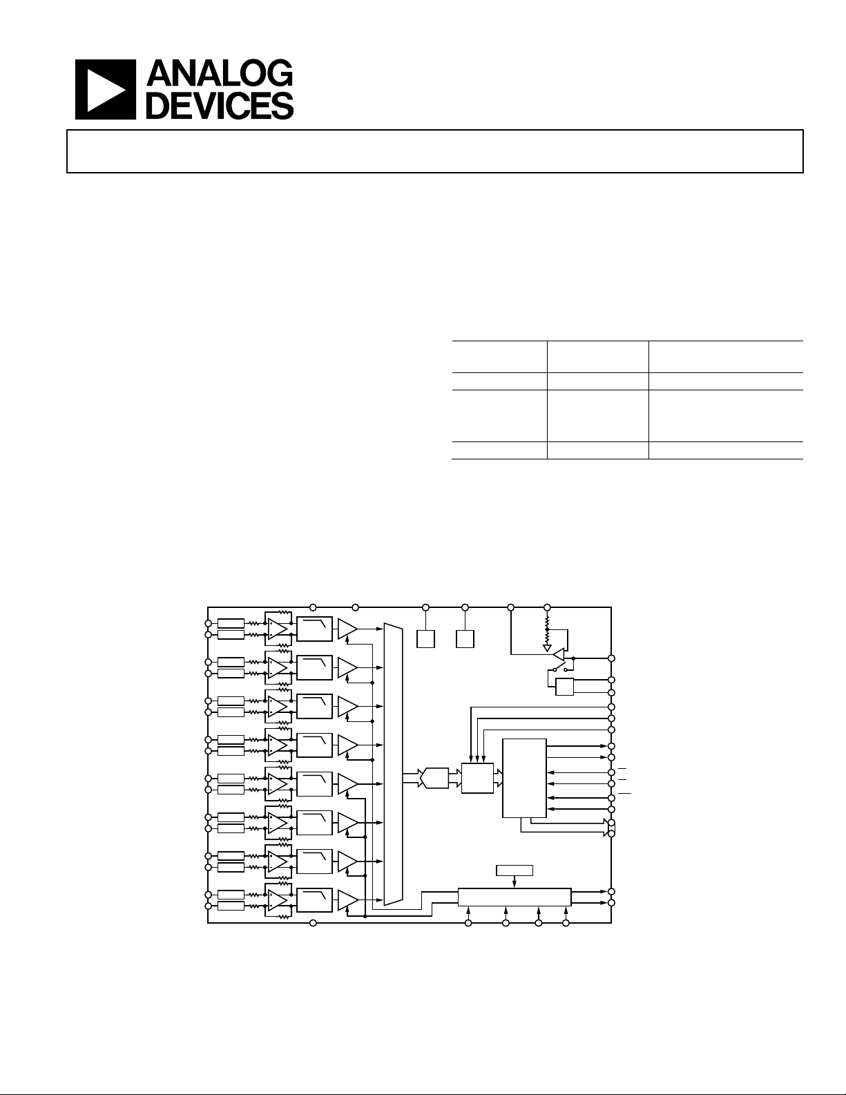
FUNCTIONAL BLOCK DIAGRAM
V
CC
CC
T/H
T/H
T/H
T/H
T/H
T/H
8:1
MUX
REGCAP
2.5V
LDO
14-BIT
SAR
REGCAP
2.5V
LDO
DIGI TAL
FILTER
REFCAPB
PARALLEL/
SERIAL
INTERFACE
REFCAPA
SERIAL
PARALLEL
2.5V
REF
REFIN/REFOUT
REF SELECT
AGND
OS 2
OS 1
OS 0
D
A
OUT
D
B
OUT
RD/SCLK
CS
PAR/SER/ BYTE SEL
V
DRIVE
DB[15:0]
AD7607
T/H
T/H
CONVST A CONVST B RESET RANGE
CLK OSC
CONTROL
INPUTS
BUSY
FRSTDATA
08096-001
Figure 1.
V1GND
V2GND
V3GND
V4GND
V5GND
V6GND
V7GND
V8GND
AV
R
1MΩ
1MΩ
1MΩ
1MΩ
1MΩ
1MΩ
1MΩ
1MΩ
1MΩ
1MΩ
1MΩ
1MΩ
1MΩ
1MΩ
1MΩ
1MΩ
R
R
R
R
R
R
R
R
R
R
R
R
R
R
R
FB
FB
FB
FB
FB
FB
FB
FB
FB
FB
FB
FB
FB
FB
FB
FB
SECOND-
ORDER LPF
SECOND-
ORDER LPF
SECOND-
ORDER LPF
SECOND-
ORDER LPF
SECOND-
ORDER LPF
SECOND-
ORDER LPF
SECOND-
ORDER LPF
SECOND-
ORDER LPF
AGND
V1
CLAMP
CLAMP
V2
CLAMP
CLAMP
V3
CLAMP
CLAMP
V4
CLAMP
CLAMP
V5
CLAMP
CLAMP
V6
CLAMP
CLAMP
V7
CLAMP
CLAMP
V8
CLAMP
CLAMP
Rev. A
Information furnished by Analog Devices is believed to be accurate and reliable. However, no
responsibility is assumed by Analog Devices for its use, nor for any infringements of patents or other
rights of third parties that may result from its use. Specifications subject to change without notice. No
license is granted by implication or otherwise under any patent or patent rights of Analog Devices.
Trademarks and registered trademarks are the property of their respective owners.
One Technology Way, P.O. Box 9106, Norwood, MA 02062-9106, U.S.A.
Tel: 781.329.4700 www.analog.com
Fax: 781.461.3113 ©2010 Analog Devices, Inc. All rights reserved.

AD7607
http://www.BDTIC.com/ADI
TABLE OF CONTENTS
Features .............................................................................................. 1
Applications ....................................................................................... 1
Functional Block Diagram .............................................................. 1
Revision History ............................................................................... 2
General Description ......................................................................... 3
Specifications ..................................................................................... 4
Timing Specifications .................................................................. 6
Absolute Maximum Ratings .......................................................... 10
Thermal Resistance .................................................................... 10
ESD Caution ................................................................................ 10
Pin Configuration and Function Descriptions ........................... 11
Typical Performance Characteristics ........................................... 14
Terminology .................................................................................... 18
Theory of Operation ...................................................................... 19
Converter Details ........................................................................ 19
Analog Input ............................................................................... 19
ADC Transfer Function ............................................................. 20
Internal/External Reference ...................................................... 21
Typical Connection Diagram ................................................... 22
Power-Down Modes .................................................................. 22
Conversion Control ................................................................... 23
Digital Interface .............................................................................. 24
Parallel Interface (
Parallel Byte Interface (
Serial Interface (
Reading During Conversion ..................................................... 25
Digital Filter ................................................................................ 26
Layout Guidelines ........................................................................... 29
Outline Dimensions ....................................................................... 31
Ordering Guide .......................................................................... 31
PA R
/SER/BYTE SEL = 0) .......................... 24
PA R
/SER/BYTE SEL = 1, DB15 = 1) .. 24
PA R
/SER/BYTE SEL = 1) ............................. 24
REVISION HISTORY
7/10—Rev. 0 to Rev. A
Change to Table 1 .............................................................................. 1
7/10—Revision 0: Initial Version
Rev. A | Page 2 of 32

AD7607
http://www.BDTIC.com/ADI
GENERAL DESCRIPTION
The AD76071 is a 14-bit, simultaneous sampling, analog-todigital data acquisition system (DAS). The part contains analog
input clamp protection; a second-order antialiasing filter; a trackand-hold amplifier; a 14-bit charge redistribution, successive
approximation analog-to-digital converter (ADC); a flexible
digital filter; a 2.5 V reference and reference buffer; and high
speed serial and parallel interfaces.
The AD7607 operates from a single 5 V supply and can accommodate ±10 V and ±5 V true bipolar input signals while sampling
at throughput rates of up to 200 kSPS for all channels. The input
1
Patent pending.
clamp protection circuitry can tolerate voltages of up to ±16.5 V.
The AD7607 has 1 MΩ analog input impedance, regardless of
sampling frequency. The single supply operation, on-chip
filtering, and high input impedance eliminate the need for
driver op amps and external bipolar supplies. The AD7607
antialiasing filter has a 3 dB cutoff frequency of 22 kHz and
provides 40 dB antialias rejection when sampling at 200 kSPS.
The flexible digital filter is pin driven and can be used to
simplify external filtering.
Rev. A | Page 3 of 32

AD7607
http://www.BDTIC.com/ADI
SPECIFICATIONS
V
= 2.5 V external/internal, AVCC = 4.75 V to 5.25 V, V
REF
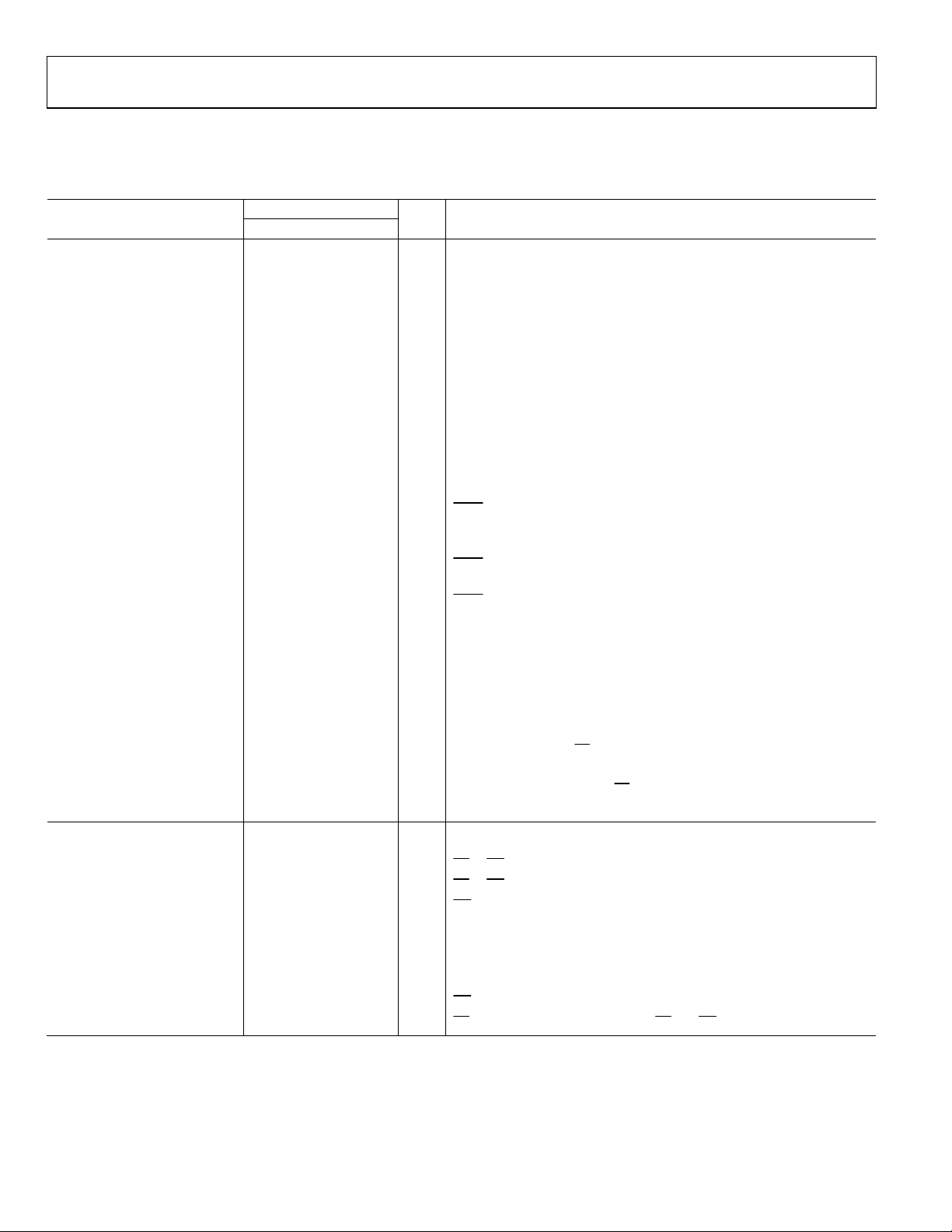
Table 2.
Parameter Test Conditions/Comments Min Typ Max Unit
DYNAMIC PERFORMANCE fIN = 1 kHz sine wave, unless otherwise noted
Signal-to-(Noise + Distortion) (SINAD)2, 3No oversampling; ±10 V range 84 84.5 dB
No oversampling; ±5 V range 83.5 84.5 dB
Signal-to-Noise Ratio (SNR)2 Oversampling by 4, fIN = 130 Hz 85.5 dB
No oversampling 84.5 dB
Total Harmonic Distortion (THD)
Peak Harmonic or Spurious Noise (SFDR)
2
−107 −95 dB
2
−108 dB
Intermodulation Distortion (IMD)2 fa = 1 kHz, fb = 1.1 kHz
Second-Order Terms −110 dB
Third-Order Terms −106 dB
Channel-to-Channel Isolation
2
f
on unselected channels up to 160 kHz −95 dB
IN
ANALOG INPUT FILTER
Full Power Bandwidth −3 dB, ±10 V range 23 kHz
−3 dB, ±5 V range 15 kHz
−0.1 dB, ±10 V range 10 kHz
−0.1 dB, ±5 V range 5 kHz
t
GROUP DELAY
±10 V Range 11 µs
±5 V Range 15 µs
DC ACCURACY
Resolution No missing codes 14 Bits
Differential Nonlinearity
Integral Nonlinearity
Positive/Negative Full-Scale Error
2
±0.25 ±0.95 LSB
2
±0.25 ±0.5 LSB
2, 5
External reference ±2 ±9 LSB
Internal reference ±2 LSB
Positive Full-Scale Error Drift
2
External reference ±2 ppm/°C
Internal reference ±7 ppm/°C
Negative Full-Scale Error Drift External reference ±4 ppm/°C
Internal reference ±8 ppm/°C
Positive/Negative Full-Scale Error
Matching
2
±10 V range 2 8 LSB
±5 V range 4 10 LSB
2, 6
Bipolar Zero Code Error
±10 V range ±0.5 ±2 LSB
±5 V range ±1 ±3.5 LSB
2
Bipolar Zero Code Error Drift
±10 V range 10 µV/°C
±5 V range 5 µV/°C
Bipolar Zero Code Error Matching ±10 V range 1 2.5 LSB
±5 V range 3 6 LSB
Total Unadjusted Error (TUE) ±10 V range ±0.5 LSB
±5 V range ±1 LSB
ANALOG INPUT
Input Voltage Ranges RANGE = 1 ±10 V
RANGE = 0 ±5 V
Input Current +10 V 5.4 µA
+5 V 2.5 µA
Input Capacitance
7
5 pF
Input Impedance See the Analog Input section 1 MΩ
= 2.3 V to 5.25 V, f
DRIVE
= 200 kSPS, TA = T
SAMPLE
MIN
to T
, unless otherwise noted.1
MAX
4
Rev. A | Page 4 of 32

AD7607
http://www.BDTIC.com/ADI
Parameter Test Conditions/Comments Min Typ Max Unit
REFERENCE INPUT/OUTPUT
Reference Input Voltage Range 2.475 2.5 2.525 V
DC Leakage Current ±1 µA
Input Capacitance
Reference Output Voltage REFIN/REFOUT
Reference Temperature Coefficient ±10 ppm/°C
LOGIC INPUTS
Input High Voltage (V
Input Low Voltage (V
Input Current (IIN) ±2 µA
Input Capacitance (CIN)7 5 pF
LOGIC OUTPUTS
Output High Voltage (VOH) I
Output Low Voltage (VOL) I
Floating-State Leakage Current ±1 ±20 µA
Floating-State Output Capacitance
Output Coding Twos complement
CONVERSION RATE
Conversion Time All eight channels included; see Tabl e 3 4 µs
Track-and-Hold Acquisition Time 1 µs
Throughput Rate All eight channels included 200 kSPS
POWER REQUIREMENTS
AVCC 4.75 5.25 V
V
2.3 5.25 V
DRIVE
I
Digital inputs = 0 V or V
TOTAL
Normal Mode (Static) 16 22 mA
Normal Mode (Operational)
Standby Mode 5 8 mA
Shutdown Mode 2 6 µA
Power Dissipation
Normal Mode (Static) 80 115.5 mW
Normal Mode (Operational) 100 142 mW
Standby Mode 25 42 mW
Shutdown Mode 10 31.5 µW
1
Temperature range for the B version is −40°C to +85°C.
2
See the Terminology section.
3
This specification applies when reading during a conversion or after a conversion. If reading during a conversion in parallel mode with V
and THD typically reduces by 3 dB.
4
LSB means least significant bit. With ±5 V input range, 1 LSB = 610.35 µV. With ±10 V input range, 1 LSB = 1.22 mV.
5
This specification includes the full temperature range variation and contribution from the internal reference buffer but does not include the error contribution from
the external reference.
6
Bipolar zero code error is calculated with respect to the analog input voltage.
7
Sample tested during initial release to ensure compliance.
8
Operational power/current figure includes contribution when running in oversampling mode.
7
REF SELECT = 1 7.5 pF
2.49/
V
2.505
) 0.9 × V
INH
) 0.1 × V
INL
= 100 µA V
SOURCE
= 100 µA 0.2 V
SINK
7
5 pF
DRIVE
8
20 27 mA
8
DRIVE
V
DRIVE
V
DRIVE
− 0.2 V
= 5 V, SNR typically reduces by 1.5 dB
DRIVE
Rev. A | Page 5 of 32
AD7607
http://www.BDTIC.com/ADI
TIMING SPECIFICATIONS
AVCC = 4.75 V to 5.25 V, V
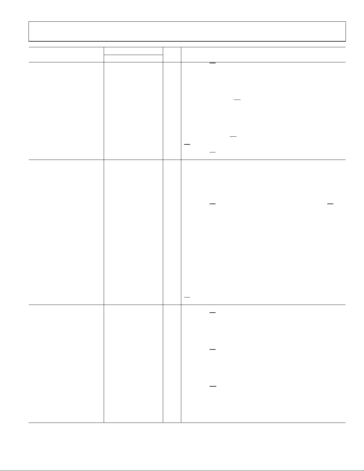
Table 3.
Limit at T
Parameter Min Typ Max Unit Description
PARALLEL/SERIAL/BYTE MODE
t
1/throughput rate
CYCLE
5 µs
5 µs Serial mode reading during conversion; V
9.1 µs Serial mode reading after a conversion; V
t
Conversion time
CONV
3.45 4 4.15 µs Oversampling off
7.87 9.1 µs Oversampling by 2
16.05 18.8 µs Oversampling by 4
33 39 µs Oversampling by 8
66 78 µs Oversampling by 16
133 158 µs Oversampling by 32
257 315 µs Oversampling by 64
t
WAKE -UP S TANDBY
t
WAKE -UP S HUTDO WN
100 µs
Internal Reference 30 ms
External Reference 13 ms
t
50 ns RESET high pulse width
RESET
t
20 ns BUSY to OS x pin setup time
OS_SETUP
t
OS_HOLD
t1 40 ns CONVST x high to BUSY high
t2 25 ns Minimum CONVST x low pulse
t3 25 ns Minimum CONVST x high pulse
t4 0 ns
2
t
5
t6 25 ns
t7 25 ns Minimum delay between RESET low to CONVST x high
PARALLEL/BYTE READ
OPERATION
t8 0 ns
t9 0 ns
t10
16 ns V
21 ns V
25 ns V
32 ns V
t11 15 ns
t12 22 ns
= 2.3 V to 5.25 V, V
DRIVE
20 ns BUSY to OS x pin hold time
0.5 ms Maximum delay allowed between CONVST A, CONVST B rising edges
= 2.5 V external reference/internal reference, TA = T
REF
, T
MIN
MAX
Parallel mode, reading during or after conversion; or serial mode (V
3.3 V to 5.25 V), reading during a conversion using D
rising edge to CONVST x rising edge; power-up time from
STBY
standby mode
rising edge to CONVST x rising edge; power-up time from
STBY
shutdown mode
rising edge to CONVST x rising edge; power-up time from
STBY
shutdown mode
BUSY falling edge to CS
Maximum time between last CS
to RD setup time
CS
to RD hold time
CS
low pulse width
RD
above 4.75 V
DRIVE
above 3.3 V
DRIVE
above 2.7 V
DRIVE
above 2.3 V
DRIVE
high pulse width
RD
high pulse width (see ); Figure 5 CS and RD linked
CS
to T
MIN
, unless otherwise noted.1
MAX
= 2.7 V
DRIVE
= 2.3 V, D
DRIVE
falling edge setup time
rising edge and BUSY falling edge
A and D
OUT
OUT
A and D
OUT
OUT
DRIVE
B lines
B lines
=
Rev. A | Page 6 of 32
AD7607
http://www.BDTIC.com/ADI
Limit at T
Parameter Min Typ Max Unit Description
t13
16 ns V
20 ns V
25 ns V
30 ns V
3
t
14
16 ns V
21 ns V
25 ns V
32 ns V
t15 6 ns
t16 6 ns
t17 22 ns
SERIAL READ OPERATION
f
Frequency of serial read clock
SCLK
23.5 MHz V
17 MHz V
14.5 MHz V
11.5 MHz V
t18
15 ns V
20 ns V
30 ns V
3
t
19
Data access time after SCLK rising edge
17 ns V
23 ns V
27 ns V
34 ns V
t20 0.4 t
t21 0.4 t
ns SCLK low pulse width
SCLK
ns SCLK high pulse width
SCLK
t22 7 SCLK rising edge to D
t23 22 ns
FRSTDATA OPERATION
t24
15 ns V
20 ns V
25 ns V
30 ns V
t25 ns
15 ns V
20 ns V
25 ns V
30 ns V
t26
16 ns V
20 ns V
25 ns V
30 ns V
MIN
, T
MAX
Delay from CS
above 4.75 V
DRIVE
above 3.3 V
DRIVE
above 2.7 V
DRIVE
above 2.3 V
DRIVE
Data access time after RD
above 4.75 V
DRIVE
above 3.3 V
DRIVE
above 2.7 V
DRIVE
above 2.3 V
DRIVE
Data hold time after RD
to DB[15:0] hold time
CS
Delay from CS
above 4.75 V
DRIVE
above 3.3 V
DRIVE
above 2.7 V
DRIVE
above 2.3 V
DRIVE
Delay from CS
until DB[15:0] three-state disabled
falling edge
falling edge
rising edge to DB[15:0] three-state enabled
until D
OUT
A/D
B three-state disabled/delay from CS
OUT
until MSB valid
above 4.75 V
DRIVE
above 3.3 V
DRIVE
= 2.3 V to 2.7 V
DRIVE
above 4.75 V
DRIVE
above 3.3 V
DRIVE
above 2.7 V
DRIVE
above 2.3 V
DRIVE
A/D
B valid hold time
OUT
B three-state enabled
OUT
rising edge to D
CS
Delay from CS
above 4.75 V
DRIVE
above 3.3 V
DRIVE
above 2.7 V
DRIVE
above 2.3 V
DRIVE
OUT
A/D
OUT
falling edge until FRSTDATA three-state disabled
Delay from CS falling edge until FRSTDATA high, serial mode
above 4.75 V
DRIVE
above 3.3 V
DRIVE
above 2.7 V
DRIVE
above 2.3 V
DRIVE
Delay from RD
above 4.75 V
DRIVE
above 3.3 V
DRIVE
above 2.7 V
DRIVE
above 2.3 V
DRIVE
falling edge to FRSTDATA high
Rev. A | Page 7 of 32
AD7607
http://www.BDTIC.com/ADI
Limit at T
Parameter Min Typ Max Unit Description
t27
19 ns V
24 ns V
t28 Delay from 16th SCLK falling edge to FRSTDATA low
17 ns V
22 ns V
t29 24 ns
1
Sample tested during initial release to ensure compliance. All input signals are specified with tR = tF = 5 ns (10% to 90% of V
2
The delay between the CONVST x signals was measured as the maximum time allowed while ensuring a <3 LSB performance matching between channel sets.
3
A buffer, which is equivalent to a load of 20 pF on the output pins, is used on the data output pins for these measurements.
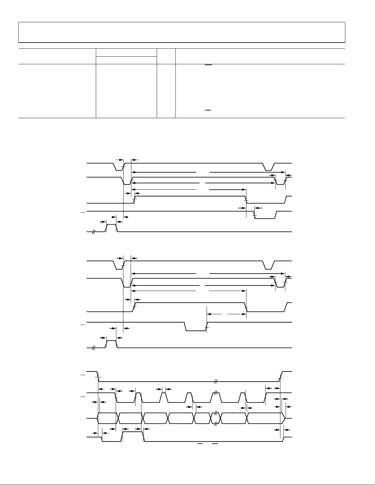
Timing Diagrams
CONVST A,
CONVST B
CONVST A,
CONVST B
BUSY
CS
RESET
CONVST A,
CONVST B
CONVST A,
CONVST B
BUSY
, T
MIN
MAX
Delay from RD
= 3.3 V to 5.25 V
DRIVE
= 2.3 V to 2.7 V
DRIVE
= 3.3 V to 5.25 V
DRIVE
= 2.3 V to 2.7 V
DRIVE
Delay from CS
t
5
t
CYCLE
t
3
t
t
1
t
7
t
RESET
Figure 2. CONVST Timing—Reading After a Conversion
t
5
t
1
CONV
t
CYCLE
t
CONV
t
3
falling edge to FRSTDATA low
rising edge until FRSTDATA three-state enabled
) and timed from a voltage level of 1.6 V.
DRIVE
t
2
t
4
08096-002
t
2
t
6
CS
RESET
t
7
t
RESET
Figure 3. CONVST Timing—Reading During a Conversion
CS
t
8
t
10
RD
DATA:
DB[15:0]
FRSTDATA
t
13
INVALID V1 V2 V3 V7 V8V4
t
26
t
24
t
11
t
14
t
27
Figure 4. Parallel Mode, Separate
Rev. A | Page 8 of 32
CS
and RD Pulses
08096-003
t
9
t
16
t
t
15
17
t
29
08096-004
AD7607
http://www.BDTIC.com/ADI
t
12
CS AND RD
t
16
t
17
DATA:
DB[15:0]
t
13
V1 V2 V3 V4 V5 V6 V7 V8
FRSTDATA
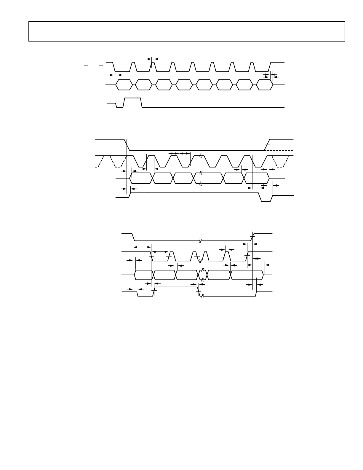
Figure 5. Linked Parallel Mode,
CS
and RD
08096-005
CS
SCLK
D
OUT
D
OUT
FRSTDATA
t
t
A,
B
18
19
DB13 DB12 DB11 DB1 DB0
t
25
t21t
20
t
22
t
28
t
23
t
29
08096-006
Figure 6. Serial Read Operation (Channel 1)
CS
RD
DATA: DB[7:0]
FRSTDATA
t
t
t
8
t
10
13
INVALID
24
HIGH
BYTE V1
t
26
t
14
LOW
BYTE V1
t
27
t
15
HIGH
BYTE V8
t
11
LOW
BYTE V8
t
29
t
9
t
16
t
17
08096-007
Figure 7. BYTE Mode Read Operation
Rev. A | Page 9 of 32
AD7607
http://www.BDTIC.com/ADI
ABSOLUTE MAXIMUM RATINGS
TA = 25°C, unless otherwise noted.
Table 4.
Parameter Rating
AVCC to AGND −0.3 V to +7 V
V
to AGND −0.3 V to AVCC + 0.3 V
DRIVE
Analog Input Voltage to AGND1 ±16.5 V
Digital Input Voltage to AGND −0.3 V to V
Digital Output Voltage to AGND −0.3 V to V
REFIN to AGND −0.3 V to AVCC + 0.3 V
Input Current to Any Pin Except Supplies1 ±10 mA
Operating Temperature Range
B Version −40°C to +85°C
Storage Temperature Range −65°C to +150°C
Junction Temperature 150°C
Pb/SN Temperature, Soldering
Reflow (10 sec to 30 sec) 240 (+ 0)°C
Pb-Free Temperature, Soldering Reflow 260 (+ 0)°C
ESD (All Pins Except Analog Inputs) 2 kV
ESD (Analog Input Pins Only) 7 kV
1
Transient currents of up to 100 mA do not cause SCR latch-up.
DRIVE
DRIVE
+ 0.3 V
+ 0.3 V
THERMAL RESISTANCE
θJA is specified for the worst-case conditions, that is, a device
soldered in a circuit board for surface-mount packages. These
specifications apply to a 4-layer board.
Table 5. Thermal Resistance
Package Type θJA θ
64-Lead LQFP 45 11 °C/W
ESD CAUTION
Stresses above those listed under Absolute Maximum Ratings
may cause permanent damage to the device. This is a stress
rating only; functional operation of the device at these or any
other conditions above those indicated in the operational
section of this specification is not implied. Exposure to absolute
maximum rating conditions for extended periods may affect
device reliability.
Unit
JC
Rev. A | Page 10 of 32
 Loading...