ANALOG DEVICES AD7490-EP Service Manual

16-Channel, 1 MSPS, 12-Bit ADC
AD7490-EP
REF
IN
V
IN
0
V
IN
15
AGND
V
DD
AD7490-EP
INPUT
MUX
12-BIT
SUCCESSIVE
APPROXIMATION
ADC
CONTROL
LOGIC
SEQUENCER
SCLK
DOUT
DIN
CS
V
DRIVE
T/H
08936-001
FEATURES
Fast throughput rate: 1 MSPS
Specified for V
Low power at maximum throughput rates
12.5 mW maximum at 1 MSPS with 5 V supplies
16 (single-ended) inputs with sequencer
Wide input bandwidth
69.5 dB SNR at 50 kHz input frequency
Flexible power/serial clock speed management
No pipeline delays
High speed serial interface, SPI/QSPI™/MICROWIRE™/
DSP compatible
Full shutdown mode: 0.5 µA maximum
28-lead TSSOP package
Support defense and aerospace applications (AQEC)
Military temperature range (−55°C to +125°C)
Controlled manufacturing baseline
One assembly/test site
One fabrication site
Enhanced product change notification
Qualification data available on request
GENERAL DESCRIPTION
The AD7490-EP is a 12-bit high speed, low power, 16-channel,
successive approximation ADC. The part operates from a single
4.75 V to 5.25 V power supply and features throughput rates up
to 1 MSPS. The part contains a low noise, wide bandwidth
track-and-hold amplifier that can handle input frequencies in
excess of 1 MHz.
The conversion process and data acquisition are controlled using
CS
and the serial clock signal, allowing the device to easily interface with microprocessors or DSPs. The input signal is sampled
on the falling edge of
point. There are no pipeline delays associated with the part.
The AD7490-EP uses advanced design techniques to achieve
very low power dissipation at high throughput rates. For
maximum throughput rates, the AD7490-EP consumes just
2.5 mA with 5 V supplies.
By setting the relevant bits in the control register, the analog input
range for the part can be selected to be a 0 V to REF
0 V to 2 × REF
ment output coding. The AD7490-EP features 16 single-ended
analog inputs with a channel sequencer to allow a preprogrammed
selection of channels to be converted sequentially. The conversion time is determined by the SCLK frequency because this is
also used as the master clock to control the conversion.
Rev. 0
Infor mation furnished by Analog Devices is believed to be accurate and reliable. However, no
responsibility is assumed by Analog Devices for its use, nor for any infringements of patents or other
rights of third parties that may result from its use. Specifications subject to change without noti ce. No
license is granted by implication or otherwise under any patent or patent rights of Analog Devices.
Trademarks and registered trademarks are the property of their respective owners.
of 4.75 V to 5.25 V
DD
CS
, and conversion is also initiated at this
IN
input, with either straight binary or twos comple-
IN
input or a
with Sequencer in 28-Lead TSSOP
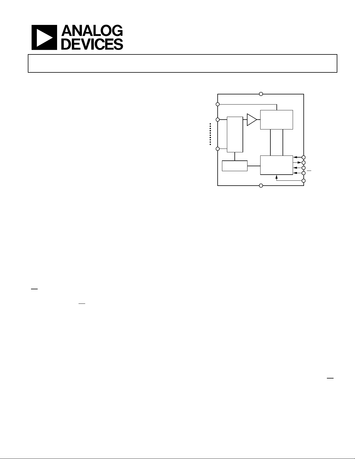
FUNCTIONAL BLOCK DIAGRAM
Figure 1.
The AD7490-EP is available in a 28-lead TSSOP package.
Full details about this enhanced product are available in the
AD7490 data sheet, which should be consulted in conjunction
with this data sheet.
PRODUCT HIGHLIGHTS
1. The AD7490-EP offers up to 1 MSPS throughput rates.
2. A sequence of channels can be selected, through which the
AD7490-EP cycles and converts.
3. The AD7490-EP operates from a single 4.75 V to 5.25 V
supply. The V
connect directly to either 3 V or 5 V processor systems
independent of V
4. The conversion rate is determined by the serial clock,
allowing the conversion time to be reduced through the
serial clock speed increase. The part also features various
shutdown modes to maximize power efficiency at lower
throughput rates. Power consumption is 0.5 µA, maximum,
when in full shutdown.
5. The part features a standard successive approximation
ADC with accurate control of the sampling instant via a
input and once off conversion control.
One Technology Way, P.O. Box 9106, Norwood, MA 02062-9106, U.S.A.
Tel: 781.329.4700
Fax: 781.461.3113 ©2010 Analog Devices, Inc. All rights reserved.
function allows the serial interface to
DRIVE
.
DD
www.analog.com
CS
 Loading...