ANALOG DEVICES AD7478A Service Manual

2.35 V to 5.25 V, 1 MSPS,
www.BDTIC.com/ADI
FEATURES
Fast throughput rate: 1 MSPS
Specified for V
Low power
3.6 mW typical at 1 MSPS with 3 V supplies
12.5 mW typical at 1 MSPS with 5 V supplies
Wide input bandwidth
71 dB SNR at 100 kHz input frequency
Flexible power/serial clock speed management
No pipeline delays
High speed serial interface
SPI®/QSPI™/MICROWIRE™/DSP compatible
Standby mode: 1 μA maximum
6-lead SC70 package
8-lead MSOP package
APPLICATIONS
Battery-powered systems
Personal digital assistants
Medical instruments
Mobile communications
Instrumentation and control systems
Data acquisition systems
High speed modems
Optical sensors
of 2.35 V to 5.25 V
DD
12-/10-/8-Bit ADCs in 6-Lead SC70
AD7476A/AD7477A/AD7478A
FUNCTIONAL BLOCK DIAGRAM
V
DD
12-/10-/8-BIT
V
T/H
IN
AD7476A/AD7477A/AD7478A
SUCCESSIVE-
APPROXIMATION
ADC
CONTROL
LOGIC
GND
Figure 1.
SCLK
SDATA
CS
02930-001
GENERAL DESCRIPTION
The AD7476A/AD7477A/AD7478A are 12-bit, 10-bit, and 8-bit
high speed, low power, successive-approximation analog-todigital converters (ADCs), respectively. The parts operate from
a single 2.35 V to 5.25 V power supply and feature throughput
rates up to 1 MSPS. The parts contain a low noise, wide
bandwidth track-and-hold amplifier that can handle input
frequencies in excess of 13 MHz. The conversion process and
data acquisition are controlled using
allowing the devices to interface with microprocessors or DSPs.
The input signal is sampled on the falling edge of
conversion is also initiated at this point. There are no pipeline
delays associated with the parts. The AD7476A/AD7477A/
AD7478A use advanced design techniques to achieve low power
dissipation at high throughput rates. The reference for the part
is taken internally from V
to allow the widest dynamic input
DD
range to the ADC. Thus, the analog input range for the part is
0 V to V
. The conversion rate is determined by the SCLK.
DD
Rev. D
Information furnished by Analog Devices is believed to be accurate and reliable. However, no
responsibility is assumed by Anal og Devices for its use, nor for any infringements of patents or ot her
rights of third parties that may result from its use. Specifications subject to change without notice. No
license is granted by implication or otherwise under any patent or patent rights of Analog Devices.
Trademarks and registered trademarks are the property of their respective owners.
CS
and the serial clock,
CS
, and the
PRODUCT HIGHLIGHTS
1. First 12-/10-/8-bit ADCs in a SC70 package.
2. H
igh throughput with low power consumption.
3. Flexi
4. Refer
5. N
One Technology Way, P.O. Box 9106, Norwood, MA 02062-9106, U.S.A.
Tel: 781.329.4700 www.analog.com
Fax: 781.461.3113 ©2006 Analog Devices, Inc. All rights reserved.
ble power/serial clock speed management. The
conversion rate is determined by the serial clock, allowing
the conversion time to be reduced through the serial clock
speed increase. This allows the average power consumption
to be reduced when a power-down mode is used while not
converting. The parts also feature a power-down mode to
maximize power efficiency at lower throughput rates.
Current consumption is 1 µA maximum and 50 nA
typically when in power-down mode.
ence derived from the power supply.
o pipeline delay. The parts feature a standard successive
approximation ADC with accurate control of the sampling
CS
instant via a
input and once-off conversion control.

AD7476A/AD7477A/AD7478A
www.BDTIC.com/ADI
TABLE OF CONTENTS
Features .............................................................................................. 1
Typical C o n ne ction D i a g ram ....................................................... 16
Applications....................................................................................... 1
Functional Block Diagram .............................................................. 1
General Description......................................................................... 1
Product Highlights........................................................................... 1
Revision History ............................................................................... 2
Specifications..................................................................................... 3
AD7476A Specifications.............................................................. 3
AD7477A Specifications.............................................................. 5
AD7478A Specifications.............................................................. 6
Timing Specifications .................................................................. 8
Absolute Maximum Ratings.......................................................... 10
ESD Caution................................................................................ 10
Pin Configurations and Function Descriptions .........................11
Typical Performance Characteristics ........................................... 12
Te r mi n ol o g y .................................................................................... 14
Theory of Operation ...................................................................... 15
Circuit Information.................................................................... 15
Analog Input............................................................................... 16
Digital Inputs .............................................................................. 17
Modes of Operation ....................................................................... 18
Normal Mode.............................................................................. 18
Power-Down Mode .................................................................... 18
Power-Up Time .......................................................................... 18
Power vs. Throughput Rate ........................................................... 20
Serial Interface................................................................................ 21
AD7478A in a 12 SCLK Cycle Serial Interface....................... 22
Microprocessor Interfacing ........................................................... 23
218xAD7476A/AD7477A/AD7478A to
DSP563xx Interface.................................................................... 24
Application Hints ........................................................................... 25
Grounding and Layout .............................................................. 25
Evaluating the AD7476A/AD7477A Performance................ 25
Outline Dimensions ....................................................................... 26
Ordering Guide .......................................................................... 26
The Converter Operation.......................................................... 15
ADC Transfer Function............................................................. 15
REVISION HISTORY
4/06—Rev. C to Rev. D
Updated Format..................................................................Universal
hanges to Ordering Guide.......................................................... 26
C
Rev. D | Page 2 of 28

AD7476A/AD7477A/AD7478A
www.BDTIC.com/ADI
SPECIFICATIONS
AD7476A SPECIFICATIONS
VDD = 2.35 V to 5.25 V, f
= 20 MHz, f
SCLK
= 1 MSPS, TA = T
SAMPLE
MIN
to T
, unless otherwise noted.
MAX
Table 1.
Parameter A Grade2 B Grade2 Y Grade2 Unit Test Conditions/Comments
DYNAMIC PERFORMANCE fIN = 100 kHz sine wave
Signal-to-Noise + Distortion (SINAD)3 70 70 70 dB min VDD = 2.35 V to 3.6 V, TA = 25°C
69 69 69 dB min VDD = 2.4 V to 3.6 V
71.5 71.5 71.5 dB typ VDD = 2.35 V to 3.6 V
69 69 69 dB min VDD = 4.75 V to 5.25 V, TA = 25°C
68 68 68 dB min VDD = 4.75 V to 5.25 V
Signal-to-Noise Ratio (SNR)3 71 71 71 dB min VDD = 2.35 V to 3.6 V, TA = 25°C
70 70 70 dB min VDD = 2.4 V to 3.6 V
70 70 70 dB min VDD = 4.75 V to 5.25 V, TA = 25°C
69 69 69 dB min VDD = 4.75 V to 5.25 V
Total Harmonic Distortion (THD)
3
–80 –80 –80 dB typ
Peak Harmonic or Spurious Noise (SFDR)3–82 –82 –82 dB typ
Intermodulation Distortion (IMD)
3
Second-Order Terms –84 –84 –84 dB typ fa = 100.73 kHz, fb = 90.72 kHz
Third-Order Terms –84 –84 –84 dB typ fa = 100.73 kHz, fb = 90.72 kHz
Aperture Delay 10 10 10 ns typ
Aperture Jitter 30 30 30 ps typ
Full Power Bandwidth 13.5 13.5 13.5 MHz typ @ 3 dB
2 2 2 MHz typ @ 0.1 dB
DC ACCURACY B and Y grades
Resolution 12 12 12 Bits
Integral Nonlinearity
3
±1.5 ±1.5 LSB max
±0.75 LSB typ
Differential Nonlinearity –0.9/+1.5 –0.9/+1.5 LSB max Guaranteed no missed codes to 12 bits
±0.75 LSB typ
Offset Error
3, 5
±1.5 ±1.5 LSB max
±1.5 ±0.2 ±0.2 LSB typ
Gain Error
3, 5
±1.5 ±1.5 LSB max
±1.5 ±0.5 ±0.5 LSB typ
Total Unadjusted Error (TUE)
3, 5
±2 ±2 LSB max
ANALOG INPUT
Input Voltage Range 0 to VDD 0 to VDD 0 to VDD V
DC Leakage Current ±0.5 ±0.5 ±0.5 A max
Input Capacitance 20 20 20 pF typ Track-and-hold in track; 6 pF typ when
in hold
LOGIC INPUTS
Input High Voltage, V
2.4 2.4 2.4 V min
INH
1.8 1.8 1.8 V min VDD = 2.35 V
Input Low Voltage, V
0.8 0.8 0.8 V max VDD = 5 V
INL
0.4 0.4 0.4 V max VDD = 3 V
Input Current, IIN, SCLK Pin ±0.5 ±0.5 ±0.5 A max Typically 10 nA, V
Input Current, IIN, CS Pin
Input Capacitance, C
6
IN
±10 ±10 ±10 nA typ
5 5 5 pF max
LOGIC OUTPUTS
Output High Voltage, VOH VDD – 0.2 VDD – 0.2 VDD – 0.2 V min I
Output Low Voltage, VOL 0.4 0.4 0.4 V max I
Floating-State Leakage Current ±1 ±1 ±1 A max
1
4
= 0 V or VDD
IN
= 200 A; VDD = 2.35 V to 5.25 V
SOURCE
= 200 A
SINK
Rev. D | Page 3 of 28

AD7476A/AD7477A/AD7478A
www.BDTIC.com/ADI
Parameter A Grade2 B Grade2 Y Grade2 Unit Test Conditions/Comments
Floating-State Output Capacitance6 5 5 5 pF max
Output Coding Straight (Natural) Binary
CONVERSION RATE
Conversion Time 800 800 800 ns max 16 SCLK cycles
Track-and-Hold Acquisition Time3 250 250 250 ns max
Throughput Rate 1 1 1 MSPS max See Serial Interface section
POWER REQUIREMENTS
VDD 2.35/5.25 2.35/5.25 2.35/5.25 V min/max
IDD Digital I/Ps = 0 V or VDD
Normal Mode (Static) 2.5 2.5 2.5 mA typ VDD = 4.75 V to 5.25 V, SCLK on or off
1.2 1.2 1.2 mA typ VDD = 2.35 V to 3.6 V, SCLK on or off
Normal Mode (Operational) 3.5 3.5 3.5 mA max VDD = 4.75 V to 5.25 V, f
1.7 1.7 1.7 mA max VDD = 2.35 V to 3.6 V, f
Full Power-Down Mode (Static) 1 1 1 μA max Typically 50 nA
Full Power-Down Mode (Dynamic) 0.6 0.6 0.6 mA typ VDD = 5 V, f
Power Dissipation7 0.3 0.3 0.3 mA typ VDD = 3 V, f
Normal Mode (Operational) 17.5 17.5 17.5 mW max VDD = 5 V, f
5.1 5.1 5.1 mW max VDD = 3 V, f
SAMPLE
SAMPLE
SAMPLE
SAMPLE
Full Power-Down Mode 5 5 5 μW max VDD = 5 V
3 3 3 μW max VDD = 3 V
1
Temperature ranges are as follows: A, B grades from –40°C to +85°C, Y grade from –40°C to +125°C.
2
Operational from VDD = 2.0 V, with input low voltage (V
3
See the Terminology section.
4
B and Y grades, maximum specifications apply as typical figures when VDD = 4.75 V to 5.25 V.
5
SC70 values guaranteed by characterization.
6
Guaranteed by characterization.
7
See the Power vs. Throughput Rate section.
) 0.35 V maximum.
INL
= 100 kSPS
= 100 kSPS
= 1 MSPS
= 1 MSPS
SAMPLE
SAMPLE
= 1 MSPS
= 1 MSPS
Rev. D | Page 4 of 28

AD7476A/AD7477A/AD7478A
www.BDTIC.com/ADI
AD7477A SPECIFICATIONS
VDD = 2.35 V to 5.25 V, f
= 20 MHz, f
SCLK
= 1 MSPS, TA = T
SAMPLE
MIN
to T
, unless otherwise noted.
MAX
Table 2.
Parameter A Grade2 Unit Test Conditions/Comments
DYNAMIC PERFORMANCE fIN = 100 kHz sine wave
Signal-to-Noise + Distortion (SINAD)
3
61 dB min
Total Harmonic Distortion (THD)3 –72 dB max
Peak Harmonic or Spurious Noise (SFDR)3 –73 dB max
Intermodulation Distortion (IMD)3
Second-Order Terms –82 dB typ fa = 100.73 kHz, fb = 90.7 kHz
Third-Order Terms –82 dB typ fa = 100.73 kHz, fb = 90.7 kHz
Aperture Delay 10 ns typ
Aperture Jitter 30 ps typ
Full Power Bandwidth 13.5 MHz typ @ 3 dB
2 MHz typ @ 0.1 dB
DC ACCURACY
Resolution 10 Bits
Integral Nonlinearity ±0.5 LSB max
Differential Nonlinearity ±0.5 LSB max Guaranteed no missed codes to 10 bits
Offset Error
Gain Error
Total Unadjusted Error (TUE)
3, 4
3, 4
3, 4
±1 LSB max
±1 LSB max
±1.2 LSB max
ANALOG INPUT
Input Voltage Range 0 to VDD V
DC Leakage Current ±0.5 µA max
Input Capacitance 20 pF typ
LOGIC INPUTS
Input High Voltage, V
2.4 V min
INH
1.8 V min VDD = 2.35 V
Input Low Voltage, V
0.8 V max VDD = 5 V
INL
0.4 V max VDD = 3 V
Input Current, IIN, SCLK Pin ±0.5 A max Typically 10 nA, VIN = 0 V or VDD
Input Current, IIN, CS Pin
Input Capacitance, C
5
IN
±10 nA typ
5 pF max
LOGIC OUTPUTS
Output High Voltage V
OH
VDD – 0.2 V min I
Output Low Voltage, VOL 0.4 V max I
Floating-State Leakage Current ±1 A max
Floating-State Output Capacitance
5
5 pF max
Output Coding Straight (Natural) Binary
CONVERSION RATE
Conversion Time 700 ns max 14 SCLK cycles with SCLK at 20 MHz
Track-and-Hold Acquisition Time
3
250 ns max
Throughput Rate 1 MSPS max
POWER REQUIREMENTS
V
DD
I
DD
2.35/5.25 V min/max
Digital I/Ps = 0 V or VDD
Normal Mode (Static) 2.5 mA typ VDD = 4.75 V to 5.25 V, SCLK on or off
1.2 mA typ VDD = 2.35 V to 3.6 V, SCLK on or off
Normal Mode (Operational) 3.5 mA max VDD = 4.75 V to 5.25 V, f
1.7 mA max VDD = 2.35 V to 3.6 V, f
1
Track-and-hold in track; 6 pF typ when in
hold
= 200 A, VDD = 2.35 V to 5.25 V
SOURCE
= 200 A
SINK
= 1 MSPS
SAMPLE
= 1 MSPS
SAMPLE
Rev. D | Page 5 of 28

AD7476A/AD7477A/AD7478A
www.BDTIC.com/ADI
Parameter A Grade2 Unit Test Conditions/Comments
Full Power-Down Mode (Static) 1 A max Typically 50 nA
Full Power-Down Mode (Dynamic) 0.6 mA typ VDD = 5 V, f
Power Dissipation
6
0.3 mA typ VDD = 3 V, f
Normal Mode (Operational) 17.5 mW max VDD = 5 V, f
5.1 mW max VDD = 3 V, f
Full Power-Down Mode 5 W max VDD = 5 V
1
Temperature range is from –40°C to +85°C.
2
Operational from V
3
See the Terminology section.
4
SC70 values guaranteed by characterization.
5
Guaranteed by characterization.
6
See the Power vs. Throughput Rate section.
= 2.0 V, with input high voltage (V
DD
) 1.8 V minimum.
INH
AD7478A SPECIFICATIONS
VDD = 2.35 V to 5.25 V, f
= 20 MHz, f
SCLK
= 1 MSPS, TA = T
SAMPLE
MIN
to T
, unless otherwise noted.
MAX
1
= 100 kSPS
SAMPLE
= 100 kSPS
SAMPLE
= 1 MSPS
SAMPLE
= 1 MSPS
SAMPLE
Table 3.
Parameter A Grade
2
Unit Test Conditions/Comments
DYNAMIC PERFORMANCE fIN = 100 kHz sine wave
Signal-to-Noise + Distortion (SINAD)
3
49 dB min
Total Harmonic Distortion (THD)3 –65 dB max
Peak Harmonic or Spurious Noise (SFDR)
Intermodulation Distortion (IMD)
3
3
–65 dB max
Second-Order Terms –76 dB typ fa = 100.73 kHz, fb = 90.7 kHz
Third-Order Terms –76 dB typ fa = 100.73 kHz, fb = 90.7 kHz
Aperture Delay 10 ns typ
Aperture Jitter 30 ps typ
Full Power Bandwidth 13.5 MHz typ @ 3 dB
2 MHz typ @ 0.1 dB
DC ACCURACY
Resolution 8 Bits
Integral Nonlinearity
Differential Nonlinearity
Offset Error
Gain Error
3, 4
3, 4
Total Unadjusted Error (TUE)
3
3
±0.3 LSB max
±0.3 LSB max Guaranteed no missed codes to eight bits
±0.3 LSB max
±0.3 LSB max
3, 4
±0.5 LSB max
ANALOG INPUT
Input Voltage Range 0 to VDD V
DC Leakage Current ±0.5 A max
Input Capacitance 20 pF typ Track-and-hold in track; 6 pF typ when
in hold
LOGIC INPUTS
Input High Voltage, V
2.4 V min
INH
1.8 V min VDD = 2.35 V
Input Low Voltage, V
0.8 V max VDD = 5 V
INL
0.4 V max VDD = 3 V
Input Current, IIN, SCLK Pin ±0.5 A max Typically 10 nA, VIN = 0 V or VDD
Input Current, IIN, CS Pin
Input Capacitance, C
5
IN
±10 nA typ
5 pF max
LOGIC OUTPUTS
Output High Voltage, V
Output Low Voltage, V
OH
OL
VDD – 0.2 V min I
0.4 V max I
= 200 A, VDD = 2.35 V to 5.25 V
SOURCE
= 200 A
SINK
Rev. D | Page 6 of 28

AD7476A/AD7477A/AD7478A
www.BDTIC.com/ADI
Parameter A Grade
2
Unit Test Conditions/Comments
Floating-State Leakage Current ±1 A max
Floating-State Output Capacitance
5
5 pF max
Output Coding Straight (Natural) Binary
CONVERSION RATE
Conversion Time 600 ns max 12 SCLK cycles with SCLK at 20 MHz
Track-and-Hold Acquisition Time
3
225 ns max
Throughput Rate 1.2 MSPS max
POWER REQUIREMENTS
VDD 2.35/5.25 V min/max
IDD Digital I/Ps = 0 V or VDD
Normal Mode (Static) 2.5 mA typ VDD = 4.75 V to 5.25 V, SCLK on or off
1.2 mA typ VDD = 2.35 V to 3.6 V, SCLK on or off
Normal Mode (Operational) 3.5 mA max VDD = 4.75 V to 5.25 V
1.7 mA max VDD = 2.35 V to 3.6 V
Full Power-Down Mode (Static) 1 A max Typically 50 nA
Full Power-Down Mode (Dynamic) 0.6 mA typ VDD = 5 V, f
Power Dissipation
6
0.3 mA typ VDD = 3 V, f
= 100 kSPS
SAMPLE
= 100 kSPS
SAMPLE
Normal Mode (Operational) 17.5 mW max VDD = 5 V
5.1 mW max VDD = 3 V
Full Power-Down Mode 5 W max VDD = 5 V
1
Temperature range is from –40°C to +85°C.
2
Operational from VDD = 2.0 V, with input high voltage (V
3
See Terminology section.
4
SC70 values guaranteed by characterization.
5
Guaranteed by characterization.
6
See the Power vs. Throughput Rate section.
) 1.8 V minimum.
INH
Rev. D | Page 7 of 28

AD7476A/AD7477A/AD7478A
www.BDTIC.com/ADI
TIMING SPECIFICATIONS
VDD = 2.35 V to 5.25 V; TA = T
MIN
to T
, unless otherwise noted.
MAX
Table 4.
Parameter Limit at T
2
f
SCLK
10 kHz min
MIN
, T
MAX
20 kHz min
20 MHz max
t
CONVER T
14 × t
12 × t
t
QUIET
16 × t
AD7476A
SCLK
AD7477A
SCLK
AD7478A
SCLK
50 ns min Minimum quiet time required between bus relinquish
and start of next conversion
t
1
10 ns min
t2 10 ns min
4
t
3
4
t
4
t5 0.4 t
t
6
5
t
7
22 ns max
40 ns max Data access time after SCLK falling edge
ns min SCLK low pulse width
SCLK
0.4 t
ns min SCLK high pulse width
SCLK
SCLK to data valid hold time
10 ns min VDD ≤ 3.3 V
9.5 ns min 3.3 V < VDD ≤ 3.6 V
7 ns min VDD > 3.6 V
6
t
8
t
7
t
POWER-UP
1
Guaranteed by characterization. All input signals are specified with tr = tf = 5 ns (10% to 90% of VDD) and timed from a voltage level of 1.6 V.
2
Mark/space ratio for the SCLK input is 40/60 to 60/40.
3
Minimum f
4
Measured with the load circuit shown in Figure 2, and defined as the time required for the output to cross 0.8 V or 1.8 V when VDD = 2.35 V, and
0.8 V or 2.0 V for VDD > 2.35 V.
5
Measured with a 50 pF load capacitor.
6
t8 is derived from the measured time taken by the data outputs to change 0.5 V when loaded with the circuit shown in Figure 2. The measured number is then
extrapolated back to remove the effects of charging or discharging the 50 pF capacitor. Therefore, the time, t8, quoted in the timing characteristics is the true bus
relinquish time of the part and is independent of the bus loading.
7
See the Power-Up Time section.
36 ns max SCLK falling edge to SDATA high impedance
values also apply to t8 minimum values ns min SCLK falling edge to SDATA high impedance
7
1 s max Power-up time from full power-down
at which specifications are guaranteed.
SCLK
1
Unit Description
3
A, B grades
3
Y grade
Minimum CS pulse width
CS
to SCLK setup time
Delay from
CS
until SDATA three-state disabled
Rev. D | Page 8 of 28

AD7476A/AD7477A/AD7478A
S
A
SCLK
www.BDTIC.com/ADI
Timing Diagrams
TO OUTPUT
PIN
C
50pF
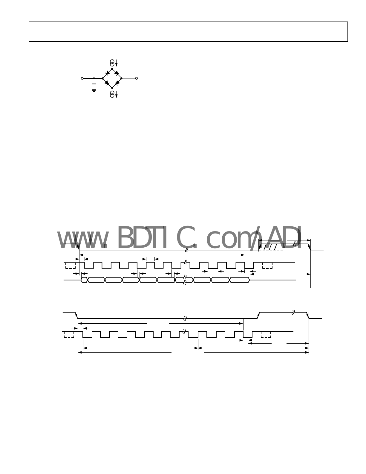
Figure 2. Load Circuit for Digital Out
Timing Example 1
Having f
= 20 MHz and a throughput of 1 MSPS, a cycle
SCLK
time of
t
+ 12.5 (1/f
2
SCLK
) + t
where:
t
= 10 ns min, leaving t
2
ACQ
requirement of 250 ns for t
From Figure 4, t
2.5 (1/f
SCLK
ACQ
) + t8 + t
is comprised of
QUIET
where:
200μA
L
200
I
OL
1.6V
I
μ
A
OH
02930-002
put Timing Specifications
= 1 µs
ACQ
to be 365 ns. This 365 ns satisfies the
.
ACQ
Timing Example 2
Having f
= 5 MHz and a throughput is 315 kSPS yields a
SCLK
cycle time of
t
+ 12.5 (1/f
2
SCLK
) + t
= 3.174 µs
ACQ
where:
= 10 ns min, this leaves t
t
2
the requirement of 250 ns for t
From Figure 4, t
2.5 (1/f
) + t8 + t
SCLK
ACQ
is comprised of
This allows a value of 128 ns for t
to be 664 ns. This 664 ns satisfies
ACQ
.
ACQ
, t8 = 36 ns maximum
QUIET
, satisfying the minimum
QUIET
requirement of 50 ns.
In this example and with other, slower clock values, the signal
ay already be acquired before the conversion is complete, but
m
it is still necessary to leave 50 ns minimum t
QUIET
between
conversions. In Example 2, acquire the signal fully at
approximately Point C in Figure 4.
t
= 36 ns maximum. This allows a value of 204 ns for t
8
satisfying the minimum requirement of 50 ns.
CS
t
STATE
2
1 3 13 14 15 16
t
3
ZERO ZERO ZERO DB11 DB10 DB2 DB1 DB0
Z
4 LEADING ZEROS
452
t
4
Figure 3. AD7476A Serial Interface Timing Diagram
t
2
12 5 13141516
34
12.5(1/f
SCLK
DAT
CS
,
QUIET
t
CONVERT
t
6
t
CONVERT
t
7
B
B
)
SCLK
1/THROUGHPUT
Figure 4. Serial Interface Timing Example
t
1
t
5
t
8
t
QUIET
THREE-STATETHREE-
02930-003
C
t
8
t
t
ACQ
QUIET
02930-004
Rev. D | Page 9 of 28
 Loading...