

V
V
www.BDTIC.com/ADI
1 MSPS, 12-/10-/8-Bit ADCs
FEATURES
Fast throughput rate: 1 MSPS
Specified for V
Low power
3.6 mW typical at 1 MSPS with 3 V supplies
15 mW typical at 1 MSPS with 5 V supplies
Wide input bandwidth
70 dB SNR at 100 kHz input frequency
Flexible power/serial clock speed management
No pipeline delays
High speed serial interface
SPI®-/QSPI™-/MICROWIRE™-/DSP-compatible
Standby mode: 1 μA maximum
6-lead SOT-23 package
APPLICATIONS
Battery-powered systems
Personal digital assistants
Medical instruments
Mobile communications
Instrumentation and control systems
Data acquisition systems
High speed modems
Optical sensors
of 2.35 V to 5.25 V
DD
in 6-Lead SOT-23
AD7476/AD7477/AD7478
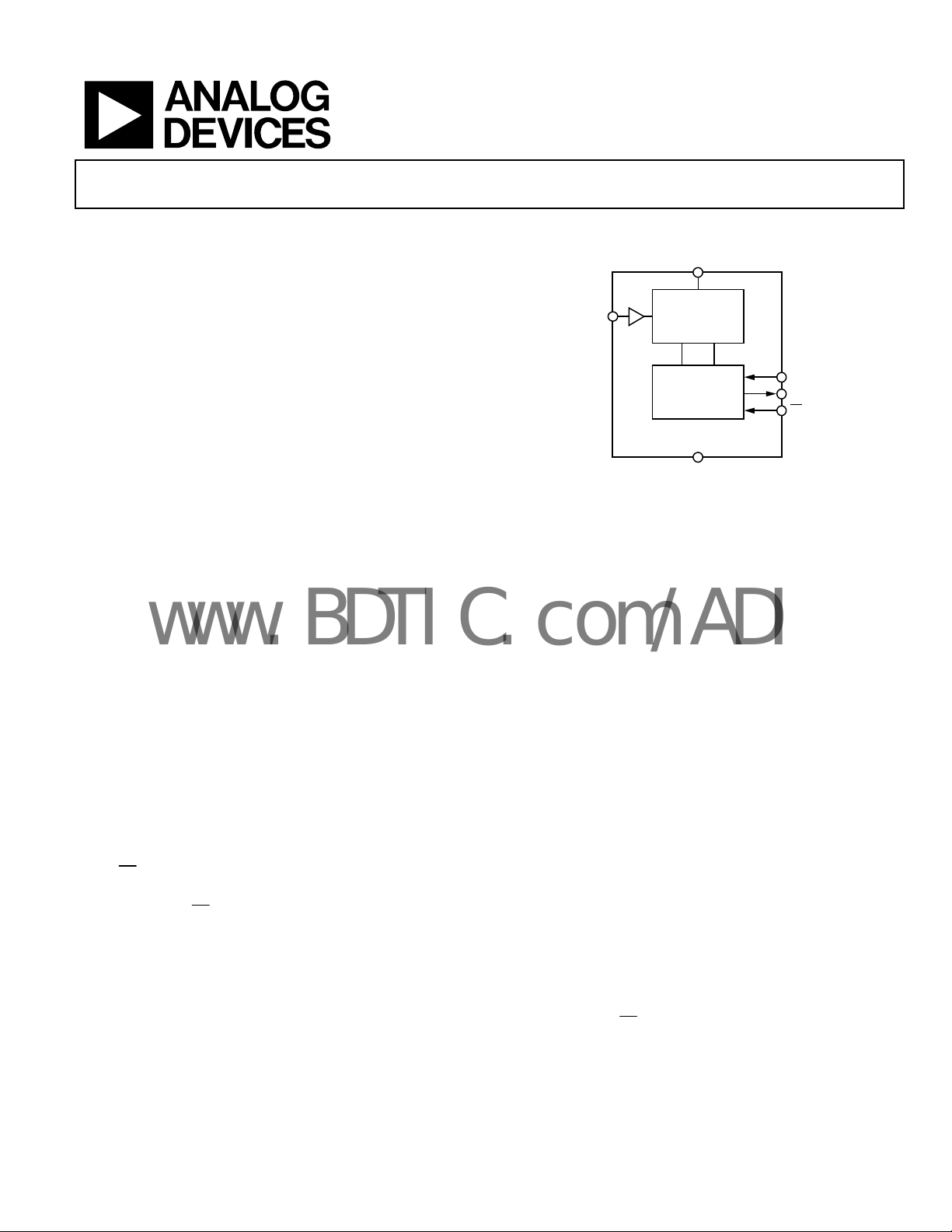
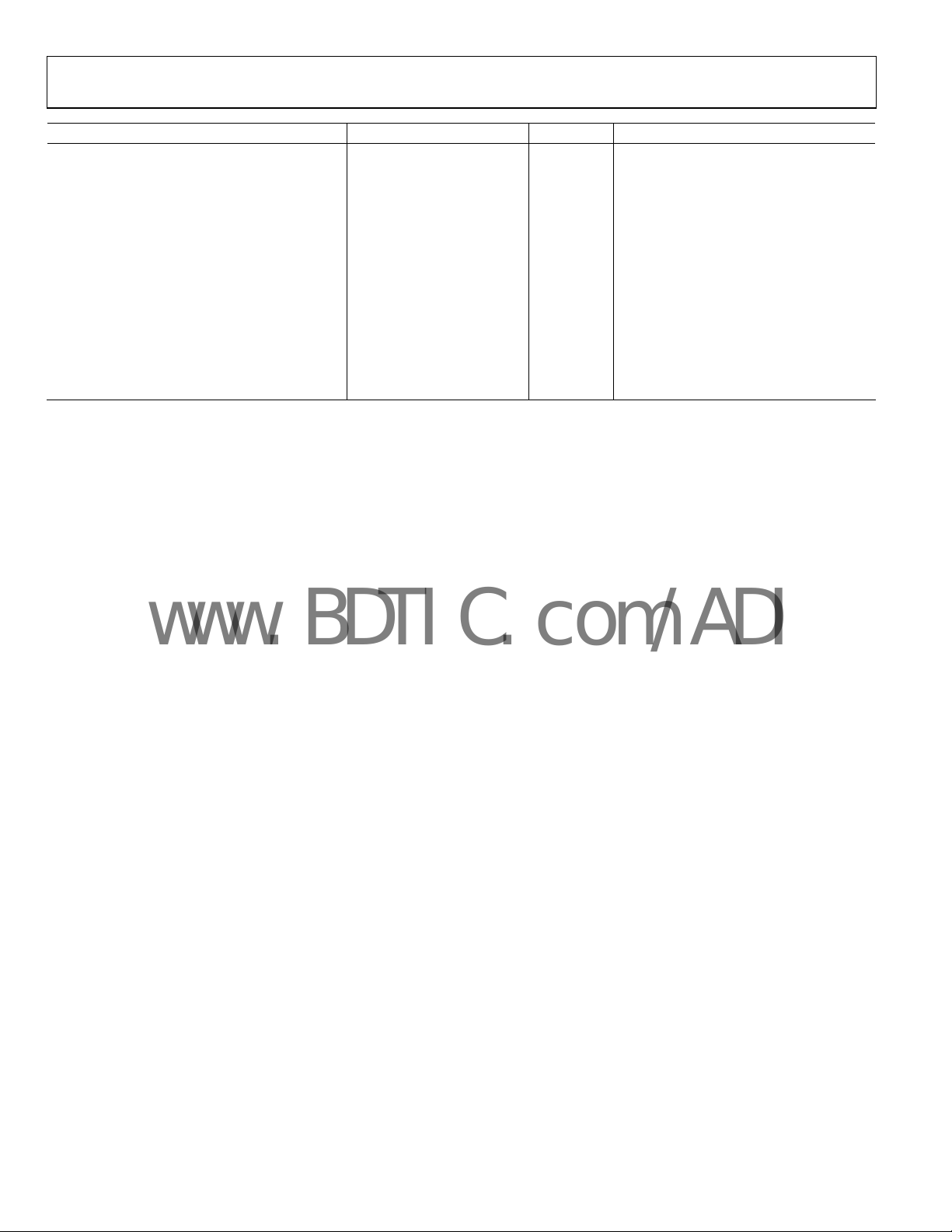
FUNCTIONAL BLOCK DIAGRAM
DD
12-/10-/8-BIT
IN
SUCCESSIVE-
APPROXIMATION
ADC
CONTROL
LOGIC
AD7476/AD7477/AD7478
GND
Figure 1.
SCLK
SDATA
CS
01024-001
GENERAL DESCRIPTION
The AD7476/AD7477/AD74781 are, respectively, 12-bit, 10-bit,
and 8-bit, high speed, low power, successive approximation
ADCs. The parts operate from a single 2.35 V to 5.25 V power
supply and feature throughput rates up to 1 MSPS. Each part
contains a low noise, wide bandwidth track-and-hold amplifier
that can handle input frequencies in excess of 6 MHz.
The conversion process and data acquisition are controlled
CS
usin
with microprocessors or DSPs. The input signal is sampled on
the falling edge of
point. There are no pipeline delays associated with these parts.
The AD7476/AD7477/AD7478 use advanced design techniques
o achieve very low power dissipation at high throughput rates.
t
The reference for the parts is taken internally from V
allows the widest dynamic input range to the ADC. Thus, the
analog input range for the parts are 0 V to V
rate is determined by the SCLK.
1
Protected by U.S. Patent No. 6,681,332.
Rev. E
Information furnished by Analog Devices is believed to be accurate and reliable. However, no
responsibility is assumed by Anal og Devices for its use, nor for any infringements of patents or ot her
rights of third parties that may result from its use. Specifications subject to change without notice. No
license is granted by implication or otherwise under any patent or patent rights of Analog Devices.
Trademarks and registered trademarks are the property of their respective owners.
and the serial clock, allowing the devices to interface
g
CS
and the conversion is initiated at this
. The conversion
DD
DD
. This
PRODUCT HIGHLIGHTS
1. First 12-/10-/8-Bit ADCs in SOT-23 Packages.
2. H
igh Throughput with Low Power Consumption.
lexible Power/Serial Clock Speed Management. The
3. F
conversion rate is determined by the serial clock, allowing
the conversion time to be reduced through the serial clock
speed increase. This allows the average power consumption
to be reduced while not converting. The parts also feature a
shutdown mode to maximize power efficiency at lower
throughput rates. Current consumption is 1 A maximum
when in shutdown mode.
4. Refer
5. N
One Technology Way, P.O. Box 9106, Norwood, MA 02062-9106, U.S.A.
Tel: 781.329.4700 www.analog.com
Fax: 781.461.3113 ©2006 Analog Devices, Inc. All rights reserved.
ence Derived from the Power Supply.
o Pipeline Delay. The parts feature a standard successiveapproximation ADC with accurate control of the sampling
instant via a
CS
input and once-off conversion control.

AD7476/AD7477/AD7478
www.BDTIC.com/ADI
TABLE OF CONTENTS
Features.............................................................................................. 1
Typical Performance Characteristics........................................... 11
Applications....................................................................................... 1
Functional Block Diagram .............................................................. 1
General Description ......................................................................... 1
Product Highlights ........................................................................... 1
Revision History ............................................................................... 2
Specifications..................................................................................... 3
AD7476 Specifications................................................................. 3
AD7477 Specifications................................................................. 5
AD7478 Specifications................................................................. 7
Timing Specifications .................................................................. 8
Absolute Maximum Ratings............................................................ 9
ESD Caution.................................................................................. 9
Pin Configuration and Function Descriptions........................... 10
Terminology.................................................................................... 12
Theory of Operation ...................................................................... 13
Circuit Information.................................................................... 13
Converter Operation.................................................................. 13
ADC Transfer Function............................................................. 13
Typical Connection Diagram ................................................... 14
Modes of Operation................................................................... 15
Power vs. Throughput Rate....................................................... 17
Serial Interface............................................................................ 18
Microprocessor Interfacing....................................................... 19
Outline Dimensions....................................................................... 21
Ordering Guide .......................................................................... 22
REVISION HISTORY
4/06—Rev. D to Rev. E
Updated Format..................................................................Universal
hanges to Table 1 Endnotes .......................................................... 3
C
Changes to Table 2 Endnotes .......................................................... 5
Changes to Table 3 Endnotes .......................................................... 7
Updated Outline Dimensions....................................................... 21
Changes to Ordering Guide.......................................................... 22
3/04—Rev. C to Rev. D
Added U.S. Patent Number ............................................................. 1
hanges to Specifications................................................................ 2
C
Changes to Absolute Maximum Ratings....................................... 6
Changes to AD7476/AD7477/AD7478 to ADSP-21xx
Interface section.............................................................................. 16
2/03—Rev. B to Rev. C
hanges to General Description .................................................... 1
C
Changes to Specifications................................................................ 2
Changes to Absolute Maximum Ratings....................................... 6
Changes to Ordering Guide............................................................ 6
Changes to Typical Connection Diagram section ..................... 10
Changes to Figure 8 caption.......................................................... 11
Changes to Figure 19...................................................................... 16
Changes to Figure 20...................................................................... 17
Updated Outline Dimensions....................................................... 18
Rev. E | Page 2 of 24
AD7476/AD7477/AD7478
www.BDTIC.com/ADI
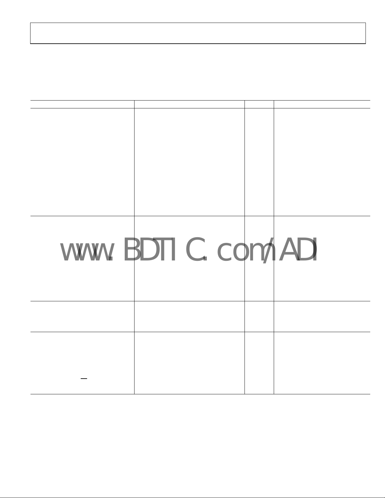
SPECIFICATIONS
AD7476 SPECIFICATIONS
A version: VDD = 2.7 V to 5.25 V, f
f
= 12 MHz, f
SCLK
= 600 kSPS, unless otherwise noted; TA = T
SAMPLE
Table 1.
Parameter A Version
DYNAMIC PERFORMANCE fIN = 100 kHz sine wave
Signal-to-(Noise + Distortion) (SINAD)3 69 70 69 dB min B version, VDD = 2.4 V to 5.25 V
70 70 dB min TA = 25°C
71.5 dB typ
Signal-to-Noise Ratio (SNR)3 70 71 70 dB min B version, VDD = 2.4 V to 5.25 V
72.5 dB typ
Total Harmonic Distortion (THD)
Peak Harmonic or Spurious Noise (SFDR)3−82 −80 −80 dB typ
Intermodulation Distortion (IMD)
Second-Order Terms −78 −78 −78 dB typ fa = 103.5 kHz, fb = 113.5 kHz
Third-Order Terms −78 −78 −78 dB typ fa = 103.5 kHz, fb = 113.5 kHz
Aperture Delay 10 10 10 ns typ
Aperture Jitter 30 30 30 ps typ
Full Power Bandwidth 6.5 6.5 6.5 MHz typ @ 3 dB
DC ACCURACY S, B versions, VDD = (2.35 V to 3.6 V)4;
A version, VDD = (2.7 V to 3.6 V)
Resolution 12 12 12 Bits
Integral Nonlinearity3 ±1.5 ±1.5 LSB max
±1 ±0.6 ±0.6 LSB typ
Differential Nonlinearity3 −0.9/+1.5 −0.9/+1.5 LSB max Guaranteed no missed codes to 12 bits
±0.75 ±0.75 ±0.75 LSB typ
Offset Error3 ±1.5 ±2 LSB max
±0.5 LSB typ
Gain Error3 ±1.5 ±2 LSB max
±0.5 LSB typ
ANALOG INPUT
Input Voltage Ranges 0 to VDD 0 to VDD 0 to VDD V
DC Leakage Current ±1 ±1 ±1 μA max
Input Capacitance 30 30 30 pF typ
LOGIC INPUT
Input High Voltage, V
1.8 1.8 1.8 V min VDD = 2.35 V
Input Low Voltage, V
0.8 0.8 0.8 V max VDD = 5 V
Input Current, IIN, SCLK Pin ±1 ±1 ±1 μA max Typically 10 nA, VIN = 0 V or VDD
Input Current, IIN, CS Pin
Input Capacitance, C
2.4 2.4 2.4 V min
INH
0.4 0.4 0.4 V max VDD = 3 V
INL
5
10 10 10 pF max
IN
= 20 MHz, f
SCLK
3
3
= 1 MSPS, unless otherwise noted; S and B versions: VDD = 2.35 V to 5.25 V,
SAMPLE
to T
MIN
1, 2
B Version
−80 −78 −78 dB typ
±1 ±1 ±1 μA typ
1,2
, unless otherwise noted.
MAX
S Version
1,2
Unit Test Conditions/Comments
Rev. E | Page 3 of 24
AD7476/AD7477/AD7478
www.BDTIC.com/ADI
Parameter A Version
1, 2
B Version
1,2
S Version
1,2
Unit Test Conditions/Comments
LOGIC OUTPUT
Output High Voltage, VOH VDD − 0.2 VDD − 0.2 VDD − 0.2 V min I
Output Low Voltage, VOL 0.4 0.4 0.4 V max I
= 200 μA; VDD = 2.35 V to 5.25 V
SOURCE
= 200 μA
SINK
Floating-State Leakage Current ±10 ±10 ±10 μA max
Floating-State Output Capacitance5 10 10 10 pF max
Output Coding Straight (Natural) Binary
CONVERSION RATE
Conversion Time 0.8 1.33 1.33 μs max 16 SCLK cycles
Track-and-Hold Acquisition Time 500 500 500 ns max Full-scale step input
350 400 400 ns max Sine wave input ≤ 100 kHz
Throughput Rate 1000 600 600 kSPS max See Serial Interface section
POWER REQUIREMENTS
VDD 2.35/5.25 2.35/5.25 2.35/5.25 V min/max
IDD Digital I/Ps = 0 V or VDD
Normal Mode (Static) 2 2 2 mA typ VDD = 4.75 V to 5.25 V, SCLK on or off
1 1 1 mA typ VDD = 2.35 V to 3.6 V, SCLK on or off
Normal Mode (Operational) 3.5 3 3 mA max
1.6 1.4 1.4 mA max
= 4.75 V to 5.25 V,
V
DD
f
= f
V
SAMPLE
DD
f
SAMPLE
SAMPLE
= 2.35 V to 3.6 V,
= f
SAMPLE
MAX6
MAX6
Full Power-Down Mode 1 1 1 μA max SCLK off
80 80 80 μA max SCLK on
Power Dissipation7
Normal Mode (Operational) 17.5 15 15 mW max VDD = 5 V, f
4.8 4.2 4.2 mW max VDD = 3 V, f
SAMPLE
SAMPLE
= f
= f
SAMPLE
SAMPLE
MAX6
MAX6
Full Power-Down 5 5 5 μW max VDD = 5 V, SCLK off
3 3 3 μW max VDD = 3 V, SCLK off
1
Temperature range for A and B versions is −40°C to +85°C; temperature range for S version is −55°C to +125°C.
2
Operational from VDD = 2.0 V.
3
See the Terminology section.
4
Maximum B and S version specifications apply as typical figures when VDD = 5.25 V.
5
Guaranteed by characterization.
6
For A version: f
7
See the Power vs. Throughput Rate section.
MAX = 1 MSPS; B and S versions: f
SAMPLE
MAX = 600 kSPS.
SAMPLE
Rev. E | Page 4 of 24
AD7476/AD7477/AD7478
www.BDTIC.com/ADI
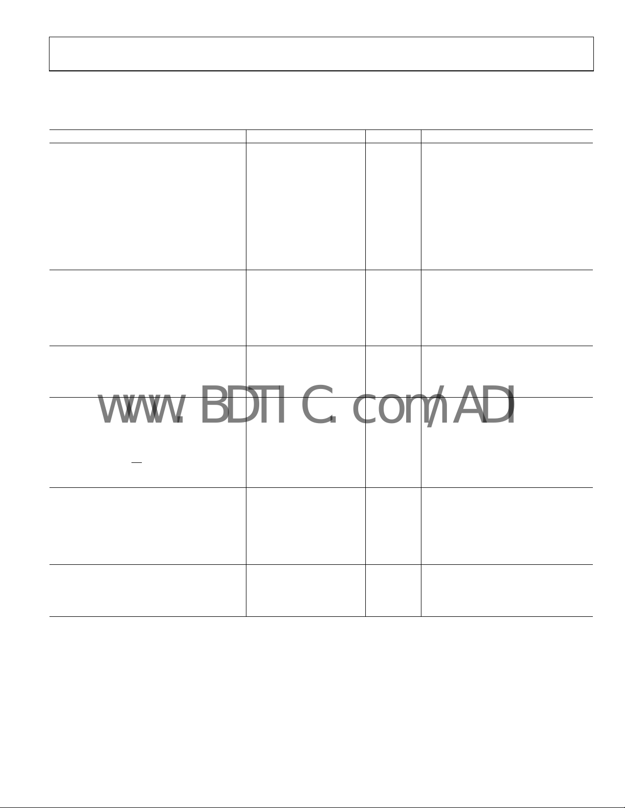
AD7477 SPECIFICATIONS
VDD = 2.7 V to 5.25 V, f
Table 2.
Parameter A Version
DYNAMIC PERFORMANCE fIN = 100 kHz sine wave, f
Signal-to-(Noise + Distortion) (SINAD) 61 61 dB min
Total Harmonic Distortion (THD)
Peak Harmonic or Spurious Noise (SFDR)3 −74 −74 dB max
Intermodulation Distortion (IMD)3
Second-Order Terms −78 −78 dB typ fa = 103.5 kHz, fb = 113.5 kHz
Third-Order Terms −78 −78 dB typ fa = 103.5 kHz, fb = 113.5 kHz
Aperture Delay 10 10 ns typ
Aperture Jitter 30 30 ps typ
Full Power Bandwidth 6.5 6.5 MHz typ @ 3 dB
DC ACCURACY
Resolution 10 10 Bits
Integral Nonlinearity
Differential Nonlinearity
Offset Error
Gain Error
3
3
ANALOG INPUT
Input Voltage Ranges 0 to VDD 0 to VDD V
DC Leakage Current ±1 ±1 μA max
Input Capacitance 30 30 pF typ
LOGIC INPUTS
Input High Voltage, V
Input Low Voltage, V
0.4 0.4 V max VDD = 3 V
Input Current, IIN, SCLK Pin ±1 ±1 μA max Typically 10 nA, VIN = 0 V or VDD
Input Current, IIN, CS Pin
Input Capacitance, C
LOGIC OUTPUTS
Output High Voltage, VOH VDD – 0.2 VDD – 0.2 V min I
Output Low Voltage, VOL 0.4 0.4 V max I
Floating-State Leakage Current ±10 ±10 μA max
Floating-State Output Capacitance4 10 10 pF max
Output Coding Straight (Natural) Binary
CONVERSION RATE
Conversion Time 800 800 ns max 16 SCLK cycles with SCLK at 20 MHz
Track-and-Hold Acquisition Time 400 400 ns max
Throughput Rate 1 1 MSPS max See Serial Interface section
= 20 MHz, TA = T
SCLK
3
3
3
MIN
to T
, unless otherwise noted.
MAX
1, 2
S Version
1,2
Unit Test Conditions/Comments
−73 −73 dB max
±1 ±1 LSB max
±0.9 ±0.9 LSB max Guaranteed no missed codes to 10 bits
±1 ±1 LSB max
±1 ±1 LSB max
2.4 2.4 V min
INH
0.8 0.8 V max VDD = 5 V
INL
±1 ±1 μA typ
4
IN
10 10 pF max
SOURCE
= 200 μA
SINK
= 1 MSPS
SAMPLE
= 200 μA, VDD = 2.7 V to 5.25 V
Rev. E | Page 5 of 24
AD7476/AD7477/AD7478
www.BDTIC.com/ADI
Parameter A Version
1, 2
S Version
1,2
Unit Test Conditions/Comments
POWER REQUIREMENTS
VDD 2.7/5.25 2.7/5.25 V min/max
IDD Digital I/Ps = 0 V or VDD
Normal Mode (Static) 2 2 mA typ VDD = 4.75 V to 5.25 V; SCLK on or off
1 1 mA typ VDD = 2.7 V to 3.6 V; SCLK on or off
Normal Mode (Operational) 3.5 3.5 mA max VDD = 4.75 V to 5.25 V; f
1.6 1.6 mA max VDD = 2.7 V to 3.6 V; f
SAMPLE
SAMPLE
= 1 MSPS
Full Power-Down Mode 1 1 μA max SCLK off
80 80 μA max SCLK on
Power Dissipation5
Normal Mode (Operational) 17.5 17.5 mW max VDD = 5 V; f
4.8 4.8 mW max VDD = 3 V; f
SAMPLE
SAMPLE
= 1 MSPS
= 1 MSPS
Full Power-Down 5 5 μW max VDD = 5 V; SCLK off
1
Temperature range for A version is −40°C to +85°C; temperature range for S version is −55°C to +125°C.
2
Operational from VDD = 2.0 V, with input high voltage, V
3
See the Terminology section.
4
Guaranteed by characterization.
5
See the Power vs. Throughput Rate section.
= 1.8 V minimum.
INH
= 1 MSPS
Rev. E | Page 6 of 24
AD7476/AD7477/AD7478
www.BDTIC.com/ADI
AD7478 SPECIFICATIONS
VDD = 2.7 V to 5.25 V, f
Table 3.
Parameter A Version
DYNAMIC PERFORMANCE fIN = 100 kHz sine wave, f
Signal-to-(Noise + Distortion) (SINAD)
Total Harmonic Distortion (THD)
Peak Harmonic or Spurious Noise (SFDR)
Intermodulation Distortion (IMD)
Second-Order Terms −68 −68 dB typ fa = 498.7 kHz, fb = 508.7 kHz
Third-Order Terms −68 −68 dB typ fa = 498.7 kHz, fb = 508.7 kHz
Aperture Delay 10 10 ns typ
Aperture Jitter 30 30 ps typ
Full Power Bandwidth 6.5 6.5 MHz typ @ 3 dB
DC ACCURACY
Resolution 8 8 Bits
Integral Nonlinearity
Differential Nonlinearity
Offset Error ±0.5 ±0.5 LSB max
Gain Error ±0.5 ±0.5 LSB max
Total Unadjusted Error (TUE) ±0.5 ±0.5 LSB max
ANALOG INPUT
Input Voltage Ranges 0 to VDD 0 to VDD V
DC Leakage Current ±1 ±1 μA max
Input Capacitance 30 30 pF typ
LOGIC INPUTS
Input High Voltage, V
Input Low Voltage, V
0.4 0.4 V max VDD = 3 V
Input Current, IIN, SCLK Pin ±1 ±1 μA max Typically 10 nA, VIN = 0 V or VDD
Input Current, IIN, CS Pin
Input Capacitance, C
LOGIC OUTPUTS
Output High Voltage, VOH VDD − 0.2 VDD − 0.2 V min I
Output Low Voltage, VOL 0.4 0.4 V max I
Floating-State Leakage Current ±10 ±10 μA max
Floating-State Output Capacitance4 10 10 pF max
Output Coding Straight (Natural) Binary
CONVERSION RATE
Conversion Time 800 800 ns max 16 SCLK cycles with SCLK at 20 MHz
Track-and-Hold Acquisition Time 400 400 ns max
Throughput Rate 1 1 MSPS max See Serial Interface section
POWER REQUIREMENTS
VDD 2.7/5.25 2.7/5.25 V min/max
IDD Digital I/Ps = 0 V or VDD
Normal Mode (Static) 2 2 mA typ VDD = 4.75 V to 5.25 V, SCLK on or off
1 1 mA typ VDD = 2.7 V to 3.6 V, SCLK on or off
Normal Mode (Operational) 3.5 3.5 mA max VDD = 4.75 V to 5.25 V, f
1.6 1.6 mA max VDD = 2.7 V to 3.6 V, f
Full Power-Down Mode 1 1 μA max SCLK off
80 80 μA max SCLK on
= 20 MHz, TA = T
SCLK
3
3
3
3
2.4 2.4 V min
INH
0.8 0.8 V max VDD = 5 V
INL
to T
MIN
3
, unless otherwise noted.
MAX
1, 2
S Version
1,2
Unit Test Conditions/Comments
49 49 dB min
−65 −65 dB max
3
−65 −65 dB max
±0.5 ±0.5 LSB max
±0.5 ±0.5 LSB max Guaranteed no missed codes to eight bits
±1 ±1 μA typ
4
10 10 pF max
IN
SOURCE
SINK
Rev. E | Page 7 of 24
= 1 MSPS
SAMPLE
= 200 μA, VDD = 2.7 V to 5.25 V
= 200 μA
= 1 MSPS
SAMPLE
= 1 MSPS
SAMPLE
AD7476/AD7477/AD7478
V
www.BDTIC.com/ADI
Parameter A Version
Power Dissipation
5
1, 2
S Version
Normal Mode (Operational) 17.5 17.5 mW max VDD = 5 V, f
4.8 4.8 mW max VDD = 3 V, f
1,2
Unit Test Conditions/Comments
= 1 MSPS
SAMPLE
= 1 MSPS
SAMPLE
Full Power-Down 5 5 μW max VDD = 5 V, SCLK off
1
Temperature range for A version is −40°C to +85°C; temperature range for S version is −55°C to +125°C.
2
Operational from VDD = 2.0 V, with input high voltage, V
3
See the Terminology section.
4
Guaranteed by characterization.
5
See the Power vs. Throughput Rate section.
= 1.8 V minimum.
INH
TIMING SPECIFICATIONS
VDD = 2.35 V to 5.25 V, TA = T
Table 4.
Limit at T
Parameter
f
SCLK
2, 3
4
3 V 5 V Unit Description
10 10 kHz min
20 20
12 12
t
16 × t
CONVER T
t
50 50 ns min Minimum quiet time required between bus relinquish and start of next conversion
QUIET
SCLK
t1 10 10 ns min
t2 10 10 ns min
5
t
3
5
t
4
20 20 ns max
40 20 ns max Data access time after SCLK falling edge, A version
70 20 ns max Data access time after SCLK falling edge, B version
t5
t6
0.4 ×
t
SCLK
0.4 ×
t
SCLK
t7 10 10 ns min SCLK to data valid hold time
6
t
10 10 ns min SCLK falling edge to SDATA high impedance
8
25 25 ns max SCLK falling edge to SDATA high impedance
7
t
1
3 V specifications apply from VDD = 2.7 V to 3.6 V for A version; 3 V specifications apply from VDD = 2.35 V to 3.6 V for B version; 5 V specifications apply from
2
Guaranteed by characterization. All input signals are specified with tr = tf = 5 ns (10% to 90% of VDD) and timed from a voltage level of 1.6 V.
3
Version A timing specifications apply to the AD7477 and AD7478 S version; B version timing specifications apply to the AD7476 S version.
4
Mark/space ratio for the SCLK input is 40/60 to 60/40.
5
Measured with the load circuit of Figure 2 and defined as the time required for the output to cross 0.8 V or 2.0 V.
6
t8 is derived from the measured time taken by the data output to change 0.5 V when loaded with the circuit in Figure 2. The measured number is then extrapolated to
7
See Power-Up Time section.
1 1 μs typ Power-up time from full power-down
POWER-UP
VDD = 4.75 V to 5.25 V.
remove the effects of charging or discharging the 50 pF capacitor. This means that the time, t
loading.
MIN
, T
MIN
16 × t
0.4 ×
t
SCLK
0.4 ×
t
SCLK
to T
MAX
, unless otherwise noted.
MAX
1
MHz
max
MHz
max
SCLK
ns min SCLK low pulsewidth
ns min SCLK high pulsewidth
A version
B version
Minimum CS
to SCLK setup time
CS
Delay from CS
pulsewidth
until SDATA three-state disabled
, is the true bus relinquish time of the part and is independent of the bus
8
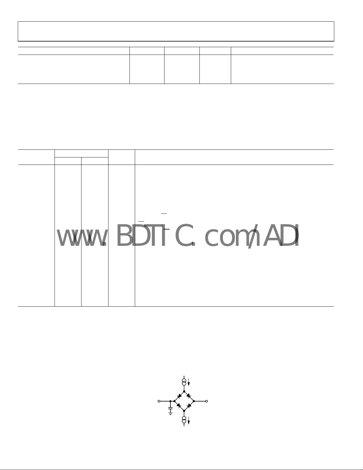
200µA I
TO OUTPUT
PIN
C
L
50pF
200µA I
Figure 2. Load Circuit for Digital Out
Rev. E | Page 8 of 24
OL
1.6
OH
01024-002
put Timing Specifications

AD7476/AD7477/AD7478
www.BDTIC.com/ADI
ABSOLUTE MAXIMUM RATINGS
TA = 25°C, unless otherwise noted.
Table 5.
Parameter Rating
VDD to GND −0.3 V to +7 V
Analog Input Voltage to GND −0.3 V to VDD + 0.3 V
Digital Input Voltage to GND −0.3 V to +7 V
Digital Output Voltage to GND −0.3 V to VDD + 0.3 V
Input Current to Any Pin Except Supplies1 ±10 mA
Operating Temperature Range
Commercial Range (A, B Versions) –40°C to +85°C
Military Range (S Version) −55°C to +125°C
Storage Temperature Range −65°C to +150°C
Junction Temperature 150°C
SOT-23 Package
θJA Thermal Impedance 230°C/W
θJC Thermal Impedance 92°C/W
Lead Temperature, Soldering Reflow
(10 sec to 30 sec) 235 (0/+5)°C
Pb-free Temperature Soldering Reflow 255 (0/+5)°C
ESD 3.5 kV
1
Transient currents of up to 100 mA do not cause SCR latch-up.
Stresses above those listed under Absolute Maximum Ratings
may cause permanent damage to the device. This is a stress
rating only; functional operation of the device at these or any
other conditions above those indicated in the operational
section of this specification is not implied. Exposure to absolute
maximum rating conditions for extended periods may affect
device reliability.
ESD CAUTION
ESD (electrostatic discharge) sensitive device. Electrostatic charges as high as 4000 V readily accumulate on
the human body and test equipment and can discharge without detection. Although this product features
proprietary ESD protection circuitry, permanent damage may occur on devices subjected to high energy
electrostatic discharges. Therefore, proper ESD precautions are recommended to avoid performance
degradation or loss of functionality.
Rev. E | Page 9 of 24

AD7476/AD7477/AD7478
www.BDTIC.com/ADI
PIN CONFIGURATION AND FUNCTION DESCRIPTIONS
V
1
DD
AD7476/
GND
AD7477/
2
AD7478
TOP VIEW
V
3
IN
(Not to Scale)
Figure 3. Pin Configuration
6
5
4
CS
SDATA
SCLK
01024-003
Table 6. Pin Function Descriptions
Pin No. Mnemonic Description
1 VDD Power Supply Input. The VDD range for the AD7476/AD7477/AD7478 is from 2.35 V to 5.25 V.
2 GND
Analog Ground. Ground reference point for all circuitry on the part. All analog input signals should be referred to this
GND voltage.
3 V
4 SCLK
Analog Input. Single-ended analog input channel. The input range is 0 V to VDD.
IN
Serial Clock. Logic input. SCLK provides the serial clock for accessing data from the part. This clock input is also used as
the clock source for the AD7476/AD7477/AD7478 conversion process.
5 SDATA
Data Out. Logic output. The conversion result is provided on this output as a serial data stream. The bits are clocked
out on the falling edge of the SCLK input. The data stream from the AD7476 consists of four leading zeros followed by
the 12 bits of conversion data; this is provided MSB first. The data stream from the AD7477 consists of four leading
zeros followed by the 10 bits of conversion data, followed by two trailing zeros, which is also provided MSB first. The
data stream from the AD7478 consists of four leading zeros followed by the eight bits of conversion data, followed by
four trailing zeros, which is provided MSB first.
6
Chip Select. Active low logic input. This input provides the dual function of initiating conversions on the
CS
AD7476/AD7477/AD7478 and framing the serial data transfer.
Rev. E | Page 10 of 24

AD7476/AD7477/AD7478
–
–
www.BDTIC.com/ADI
TYPICAL PERFORMANCE CHARACTERISTICS
0
–10
–20
–30
–40
–50
SNR (dB)
–60
–70
–80
–90
0 50045040035030025020015010050
FREQUENCY (kHz)
Figure 7. AD7478 Dynamic Performance at 1 MSPS
8192 POINT FFT
f
= 1MSPS
SAMPLE
f
= 100kHz
IN
SINAD = 49.82dB
THD = –75.22d B
SFDR = –67.78d B
01024-007
–15
–35
–55
SNR (dB)
–75
–95
–115
0 50045040035030025020015010050
FREQUENCY (kHz)
Figure 4. AD7476 Dynamic Performance at 1 MSPS
8192 POINT FFT
f
= 1MSPS
SAMPLE
f
= 100kHz
IN
SINAD = 71.67dB
THD = –81.00d B
SFDR = –81.63d B
01024-004
–15
–35
–55
SNR (dB)
–75
–95
–115
0 30025020015010050
FREQUENCY (kHz)
Figure 5. AD7476 Dynamic Performance at 600 kSPS
0
–10
–20
–30
–40
–50
SNR (dB)
–60
–70
–80
–90
–100
0 50045040035030025020015010050
FREQUENCY (kHz)
Figure 6. AD7477 Dynamic Performance at 1 MSPS
8192 POINT FFT
f
= 600kSPS
SAMPLE
f
= 100kHz
IN
SINAD = 71.71dB
THD = –80.88d B
SFDR = –83.23d B
8192 POINT FFT
f
= 1MSPS
SAMPLE
f
= 100kHz
IN
SINAD = 61.66dB
THD = –80.64d B
SFDR = –85.75d B
66
SCLK = 20MHz
–67
–68
–69
–70
SINAD (dB)
–71
–72
01024-005
–73
10k 1M100k
V
DD
INPUT FREQUENCY (kHz)
= 5.25V
VDD = 2.35V
V
= 3.6V
V
DD
DD
= 2.7V
V
DD
= 4.75V
01024-008
Figure 8. AD7476 SINAD vs. Input Frequency at 993 kSPS
69.0
SCLK = 12MHz
–69.5
–70.0
–70.5
–71.0
SINAD (dB)
–71.5
–72.0
01024-006
–72.5
10k 1M100k
INPUT FREQ UENCY (kHz)
VDD = 2.35V
= 2.7V
V
DD
V
= 5.25V
DD
V
= 4.75V
DD
= 3.6V
V
DD
01024-009
Figure 9. AD7476 SINAD vs. Input Frequency at 605 kSPS
Rev. E | Page 11 of 24

AD7476/AD7477/AD7478
www.BDTIC.com/ADI
TERMINOLOGY
Integral Nonlinearity
This is the maximum deviation from a straight line passing
rough the endpoints of the ADC transfer function. For the
th
AD7476/AD7477, the endpoints of the transfer function are
zero scale, a point ½ LSB below the first code transition, and
full scale, a point ½ LSB above the last code transition. For the
AD7478, the endpoints of the transfer function are zero scale, a
point 1 LSB below the first code transition, and full scale, a
point 1 LSB above the last code transition.
Differential Nonlinearity
This is the difference between the measured and the ideal 1 LSB
ange between any two adjacent codes in the ADC.
ch
Offset Error
This is the deviation of the first code transition (00 . . . 000) to
(00 . . . 001) f
AD7478, this is the deviation of the first code transition
(00 . . . 000) to (00 . . . 001) from the ideal (such as
AGND + 1 LSB).
Gain Error
For the AD7476/AD7477, this is the deviation of the last code
tra
nsition (111 . . . 110) to (111 . . . 111) from the ideal (such as
V
– 1.5 LSB) after the offset error has been adjusted out. For
REF
the AD7478, this is the deviation of the last code transition
(111 . . . 110) to (111 . . . 111) from the ideal (such as V
LSB) after the offset error has been adjusted.
Track-and-Hold Acquisition Time
The track-and-hold amplifier returns into track mode after the
end o
required for the output of the track-and-hold amplifier to reach
its final value, within ±0.5 LSB, after the end of conversion. See
the
Serial Interface section for more details.
Signal-to-(Noise + Distortion) Ratio
This is the measured ratio of signal-to-(noise + distortion) at
he output of the ADC. The signal is the rms amplitude of the
t
fundamental. Noise is the sum of all nonfundamental signals up
to half the sampling frequency (f
The ratio is dependent on the number of quantization levels in
he digitization process; the more levels, the smaller the
t
quantization noise. The theoretical signal-to-(noise +
distortion) ratio for an ideal N-bit converter with a sine wave
input is given by
Signal-to-(Noise + Distortion) = (6.02
rom the ideal (such as AGND + 0.5 LSB). For the
– 1
REF
f conversion. Track-and-hold acquisition time is the time
/2), excluding dc.
S
N + 1.76) dB
Thus, for a 12-bit converter, this is 74 dB; for a 10-bit converter
t is 62 dB; and for an 8-bit converter it is 50 dB.
i
Tot a l U n ad ju s te d E rr o r
This is a comprehensive specification that includes gain error,
arity error, and offset error.
line
Total Harmonic Distortion (THD)
Total harmonic distortion is the ratio of the rms sum of
rmonics to the fundamental. For the AD7476/
ha
AD7477/AD7478, it is defined as:
2
()
THD
where V
, V5, and V6 are the rms amplitudes of the second through the
V
4
=
is the rms amplitude of the fundamental and V2, V3,
1
2
log20dB
4
3
V
1
VVVVV
++++
5
6
2
2
2
2
sixth harmonics.
Peak Harmonic or Spurious Noise
Peak harmonic or spurious noise is defined as the ratio of the
ms value of the next largest component in the ADC output
r
spectrum (up to f
/2 and excluding dc) to the rms value of the
S
fundamental. Normally, the value of this specification is
determined by the largest harmonic in the spectrum, but for
ADCs where the harmonics are buried in the noise floor, it is
a noise peak.
Intermodulation Distortion
With inputs consisting of sine waves at two frequencies, fa and
, any active device with nonlinearities creates distortion
fb
products at sum and difference frequencies of mfa ± nfb where
m, n = 0, 1, 2, 3, and so on. Intermodulation distortion terms
are those for which neither m nor n is equal to zero. For
example, the second-order terms include (fa + fb) and (fa − fb),
while the third-order terms include (2fa + fb), (2fa − fb),
(fa + 2fb), and (fa − 2fb).
The AD7476/AD7477/AD7478 are tested using the CCIF
s
tandard where two input frequencies are used (fa = 498.7 kHz
and fb = 508.7 kHz). In this case, the second-order terms are
usually distanced in frequency from the original sine waves
while the third-order terms are usually at a frequency close to
the input frequencies. As a result, the second- and third-order
terms are specified separately. The calculation of the
intermodulation distortion is as per the THD specification
where it is the ratio of the rms sum of the individual distortion
products to the rms amplitude of the sum of the fundamentals,
expressed in dB.
Rev. E | Page 12 of 24

AD7476/AD7477/AD7478
V
www.BDTIC.com/ADI
THEORY OF OPERATION
CIRCUIT INFORMATION
The AD7476/AD7477/AD7478 are, respectively, 12-bit, 10-bit,
and 8-bit, fast, micropower, single-supply ADCs. The parts can
be operated from a 2.35 V to 5.25 V supply. When operated
from either a 5 V supply or a 3 V supply, the AD7476/AD7477/
AD7478 are capable of throughput rates of 1 MSPS when
provided with a 20 MHz clock.
AGND
SAMPLING
A
CAPACITOR
B
CONVERSION
PHASE
COMPARATOR
SW2
VDD/2
V
IN
SW1
Figure 11. ADC Conversion Phase
CHARGE
REDISTRIBUT ION
DAC
CONTROL
LOGIC
01024-011
Each AD7476/AD7477/AD7478 provides an on-chip, tracka
nd-hold ADC and a serial interface housed in a tiny 6-lead
SOT-23 package, which offers considerable space-saving
advantages. The serial clock input accesses data from the part
and provides the clock source for the successive-approximation
ADC. The analog input range is 0 V to V
. An external
DD
reference is not required for the ADC, nor is there a reference
on-chip. The reference for the AD7476/AD7477/AD7478 is
derived from the power supply and thus provides the widest
dynamic input range.
The AD7476/AD7477/AD7478 also feature a power-down
ion to save power between conversions. The power-down
opt
feature is implemented across the standard serial interface as
described in the Modes of Operation section.
CONVERTER OPERATION
The AD7476/AD7477/AD7478 are successive-approximation
analog-to-digital converters based around a charge redistribution DAC. Figure 1 and Figure 11 show simplified schematics
of
the ADC. Figure 10 shows the ADC during its acquisition
p
hase. SW2 is closed and SW1 is in Position A, the comparator
is held in a balanced condition, and the sampling capacitor
acquires the signal on V
IN
A
AGND
CAPACITO R
B
ACQUISITION
SW1
.
IN
SAMPLING
PHASE
VDD/2
COMPARAT OR
SW2
Figure 10. ADC Acquisition Phase
CHARGE
REDISTRIBUTIO N
DAC
CONTROL
LOGIC
01024-010
ADC TRANSFER FUNCTION
The output coding of the AD7476/AD7477/AD7478 is straight
binary. For the AD7476/AD7477, designed code transitions
occur midway between successive integer LSB values, such as ½
LSB, 1½ LSB, and so on. The LSB size for the AD7476 is
V
/4096, and the LSB size for the AD7477 is VDD/1024. The
DD
ideal transfer characteristic for the AD7476/AD7477 is shown
in
Figure 12.
For the AD7478, designed code transitions occur midway
be
tween successive integer LSB values, such as 1 LSB, 2 LSB,
and so on. The LSB size for the AD7478 is V
transfer characteristic for the AD7478 is shown in Figure 13.
111 ... 111
111 ... 110
111 ... 000
ADC CODE
011 ... 111
000 ... 010
000 ... 001
000 ... 000
0.5LSB +V
0V
Figure 12. Transfer Characteristic for the AD7476/AD7477
111 ... 111
111 ... 110
1LSB = VDD/4096 (AD7476)
1LSB = V
ANALOG I NPUT
/256. The ideal
DD
/1024 (AD7477)
DD
– 1.5LSB
DD
01024-012
When the ADC starts a conversion (see Figure 11), SW2 opens
and SW1 moves to Position B, causing the comparator to
become unbalanced. The control logic and the charge redistri-
111 ... 000
ADC CODE
011 ... 111
bution DAC are used to add and subtract fixed amounts of
charge from the sampling capacitor to bring the comparator
back into a balanced condition. When the comparator is rebalanced, the conversion is complete. The control logic generates
the ADC output code.
tra
nsfer function.
Figure 12 and Figure 13 show the ADC
Rev. E | Page 13 of 24
000 ... 010
000 ... 001
000 ... 000
1LSB +V
0V
Figure 13. Transfer Characteristic for AD7478
1LSB = VDD/256 (AD7478)
ANALOG I NPUT
DD
– 1LSB
01024-013

AD7476/AD7477/AD7478
Y
V
V
www.BDTIC.com/ADI
TYPICAL CONNECTION DIAGRAM
Figure 14 shows a typical connection diagram for the
AD7476/AD7477/AD7478. V
and as such, V
should be well decoupled. This provides an
DD
analog input range of 0 V to V
output in a 16-bit word with four leading zeros followed by the
MSB of the 12-bit, 10-bit, or 8-bit result. The 10-bit result from
the AD7477 is followed by two trailing zeros. The 8-bit result
from the AD7478 is followed by four trailing zeros.
Alternatively, because the supply current required by the
AD7476/AD74
77/AD7478 is so low, a precision reference can
be used as the supply source to the part. A REF19x voltage
reference (
pply the required voltage to the ADC (see Figure 14). This
su
co
nfiguration is especially useful if the power supply is quite
REF195 for 5 V or REF193 for 3 V) can be used to
noisy or if the system supply voltages are at some value other
than 5 V or 3 V, such as 15 V.
The REF19x outputs a steady voltage to the AD7476/
AD7477/AD74
78. If the low dropout REF193 is used, the
current it typically needs to supply to the AD7476/AD7477/
AD7478 is 1 mA. When the ADC is converting at a rate of
1 MSPS, the REF193 needs to supply a maximum of 1.6 mA to
the AD7476/AD7477/AD7478. The load regulation of the
REF193 is typically 10 ppm/mA (REF193, V
results in an error of 16 ppm (48 µV) for the 1.6 mA drawn
from it. This corresponds to a 0.065 LSB error for the AD7476
with V
= 3 V from the REF193, a 0.016 LSB error for the
DD
AD7477, and a 0.004 LSB error for the AD7478.
For applications where power consumption is of concern, the
ower-down mode of the ADC and the sleep mode of the
p
REF19x reference should be used to improve power performance. See the Modes of Operation section.
1mA
1µF
TANT
V
DD
AD7476/
V
IN
AD7477/
AD7478
GND
Figure 14. REF193 as Power Supply
0V TO V
INPUT
690nF
DD
Tabl e 7 provides some typical performance data with various
references used as a V
source with a low frequency analog
DD
input. Under the same setup conditions, the references are
compared and the AD780 proved the optimum reference.
is taken internally from VDD
REF
. The conversion result is
DD
= 5 V), which
S
3V
0.1µF
SCLK
SDATA
REF193
CS
SERIAL
INTERFACE
10µF 10µF
µC/µP
5V
SUPPL
Table 7.
AD7476 SNR Performance
Reference Tied to VDD
1 kH
z Input (dB)
AD780 @ 3 V 71.17
REF193 70.4
AD780 @ 2.5 V 71.35
REF192 70.93
AD1582 70.05
Analog Input
Figure 15 shows an equivalent circuit of the analog input
structure of the AD7476/AD7477/AD7478. The two diodes, D1
and D2, provide ESD protection for the analog input. Take care
to ensure that the analog input signal never exceeds the supply
rails by more than 300 mV. This causes these diodes to become
forward-biased and start conducting current into the substrate.
These diodes can conduct a maximum of 10 mA without
causing irreversible damage to the part.
The Capacitor C1 in Figure 15 is typically about 4 pF and can
pr
imarily be attributed to pin capacitance. The Resistor R1 is a
lumped component made up of the on resistance of a switch.
This resistor is typically about 100 . The Capacitor C2 is the
ADC sampling capacitor and typically has a capacitance of
30 pF. For ac applications, removing high frequency components from the analog input signal is recommended by use of a
band-pass filter on the relevant analog input pin. In applications
where harmonic distortion and signal-to-noise ratio are critical,
the analog input should be driven from a low impedance
source. Large source impedances significantly affect the ac
performance of the ADC. This may necessitate using an input
buffer amplifier. The choice of the op amp is a function of the
particular application.
DD
D1
IN
C1
4pF
Figure 15. Equivalent Analog Input Circuit
D2
CONVERSAION PHASE—SWITCH O PEN
TRACK PHASE—SWI TCH CLOSED
C2
30pF
R1
01024-015
When no amplifier is used to drive the analog input, the source
impedance should be limited to low values. The maximum
01024-014
source impedance depends on the amount of total harmonic
distortion (THD) that can be tolerated. The THD increases as
the source impedance increases and performance degrades.
Figure 16 shows a graph of the total harmonic distortion versus
ource impedance for different analog input frequencies when
s
using a supply voltage of 2.7 V and sampling at a rate of
605 kSPS.
tot
Figure 17 and Figure 18 each show a graph of the
al harmonic distortion vs. analog input signal frequency for
various supply voltages while sampling at 993 kSPS with an
SCLK frequency of 20 MHz and 605 kSPS with an SCLK
frequency of 12 MHz, respectively.
Rev. E | Page 14 of 24

AD7476/AD7477/AD7478
–
–
www.BDTIC.com/ADI
0
–10
–20
–30
–40
–50
THD (dB)
–60
–70
–80
–90
–100
1 10k1k10010
f
= 300kHz
IN
f
= 10kHz
IN
SOURCE IMPEDANCE (Ω)
= 2.7V
V
DD
f
= 605kSPS
S
f
= 200kHz
IN
f
= 100kHz
IN
Figure 16. THD vs. Source Impedance for Various Analog Input Frequencies
50
–55
–60
–65
V
–70
THD (dB)
–75
–80
–85
–90
10k 1M100k
INPUT FREQ UENCY (Hz)
DD
Figure 17. THD vs. Analog Input Frequency, f
72
–74
= 5.25V
V
V
DD
= 993 kSPS
s
VDD = 2.35V
VDD = 2.35V
= 2.7V
V
DD
= 4.75V
DD
= 3.6V
Digital Input
The digital input applied to the AD7476/AD7477/AD7478 is
not limited by the maximum ratings that limit the analog input.
Instead, the digital input applied can go to 7 V and is not
restricted by the V
+ 0.3 V limit as on the analog input. For
DD
example, if the AD7476/AD7477/AD7478 are operated with a
V
of 3 V, then 5 V logic levels can be used on the digital input.
DD
However, note that the data output on SDATA still has 3 V logic
levels when V
being restricted by the V
sequencing issues are avoided. If
01024-016
V
, there is no risk of latch-up as there is on the analog input
DD
when a signal greater than 0.3 V is applied prior to V
= 3 V. Another advantage of SCLK and CS not
DD
+ 0.3 V limit is that power supply
DD
CS
or SCLK is applied before
.
DD
MODES OF OPERATION
Select the mode of operation of the AD7476/AD7477/AD7478
by controlling the (logic) state of the
conversion. The two possible modes of operation are normal
mode and power-down mode. The point at which
high after the conversion has been initiated determines whether
or not the AD7476/AD7477/AD7478 enters power-down mode.
Similarly, if already in power-down,
device returns to normal operation or remains in power-down.
These modes of operation are designed to provide flexible
power management options. These options can be chosen to
optimize the power dissipation/throughput rate ratio for
01024-017
different application requirements.
Normal Mode
This mode is intended for fastest throughput rate performance.
Users do not have to worry about power-up times with the
AD7476/AD7477/AD7478 remaining fully powered at all times.
Figure 19 shows the general diagram of the AD7476/AD7477/
AD7478
in normal mode.
CS
signal during a
CS
is pulled
CS
can control whether the
–76
The conversion is initiated on the falling edge of
scribed in the Serial Interface section. To ensure the part
r
–78
THD (dB)
–80
–82
–84
10k 1M100k
INPUT FREQ UENCY (Hz)
Figure 18. THD vs. Analog Input Frequency, f
VDD = 2.7V
VDD = 4.75V
VDD = 5.25V
= 3.6V
V
DD
= 605 kSPS
s
01024-018
emains fully powered up at all times,
at least 10 SCLK falling edges have elapsed after the falling edge
CS
of
. If CS is brought high any time after the tenth SCLK
falling edge, but before the sixteenth SCLK falling edge, the part
remains powered up, but the conversion terminates and SDATA
goes back into three-state. Sixteen serial clock cycles are
required to complete the conversion and access the complete
conversion result.
may idle low until
CS
may idle high until the next conversion or
CS
returns high sometime prior to the next
conversion (effectively idling
Once a data transfer is complete, (SDATA has returned to three-
tate), another conversion can be initiated after the quiet time,
s
t
, has elapsed by again bringing CS low.
QUIET
Rev. E | Page 15 of 24
CS
low).
CS
as de-
CS
must remain low until

AD7476/AD7477/AD7478
S
A
S
A
www.BDTIC.com/ADI
Power-Down Mode
This mode is intended for use in applications where slower
throughput rates are required; either the ADC is powered
between each conversion, or a series of conversions can be
performed at a high throughput rate and the ADC is then
powered down for a relatively long duration between these
bursts of several conversions. When the AD7476/AD7477/
AD7478 is in power-down mode, all analog circuitry is
powered down.
To enter power-down, the conversion process must be
CS
i
nterrupted by bringing
falling edge of SCLK and before the tenth falling edge of SCLK,
as shown in
Figure 20. Once
of SCLKs, the part enters power-down and the conversion
initiated by the falling edge of
goes back into three-state.
high any time after the second
CS
is brought high in this window
CS
is terminated and SDATA
CS
CS
is brought high before the second SCLK falling edge, the
If
part remains in normal mode and does not power down. This
CS
avoids accidental power-down due to glitches on the
line.
To exit this mode of operation and power up the AD7476/
AD7477/AD74
falling edge of
to power up as long as
78 again, perform a dummy conversion. On the
CS
, the device begins to power up, and continues
CS
is held low until after the falling edge
of the tenth SCLK. The device is fully powered up once 16
SCLKs have elapsed and, as shown in Figure 21, valid data
results from the next conversion. If
CS
is brought high before
the tenth falling edge of SCLK, the AD7476/AD7477/AD7478
again goes back into power-down. This avoids accidental
power-up due to glitches on the
of eight SCLK cycles while
begin to power up on the falling edge of
again on the rising edge of
CS
line or an inadvertent burst
CS
is low. Although the device may
CS
, it powers down
CS
as long as it occurs before the
tenth SCLK falling edge.
CS
SCLK
SDATA
THE PART BEGI NS
TO POW ER UP
A
1 10 16
SCLK
DAT
CS
SCLK
DAT
INVALID DATA VALID DATA
4 LEADING Z EROS + CONVE RSION RESUL T
Figure 19. Normal Mode Operation
110162
Figure 20. Entering Power-Down Mode
16101 161
Figure 21. Exiting Power-Down Mode
THREE-STATE
THE PART IS FULL Y POWERED
UP WITH V
FULLY ACQUIRED
IN
01024-019
01024-020
01024-021
Rev. E | Page 16 of 24

AD7476/AD7477/AD7478
www.BDTIC.com/ADI
Power-Up Time
The power-up time of the AD7476/AD7477/AD7478 is typically 1 µs, which means that with any frequency of SCLK up to
20 MHz, one dummy cycle is always sufficient to allow the
device to power up. Once the dummy cycle is complete, the
ADC is fully powered up and the input signal is acquired
properly. The quiet time (t
) must still be allowed from the
QUIET
point at which the bus goes back into three-state (after the
dummy conversion), to the next falling edge of
CS
. When
running at 1 MSPS throughput rate, the AD7476/AD7477/
AD7478 powers up and acquires a signal within ±0.5 LSB in
one dummy cycle, such as 1 µs.
When powering up from the power-down mode with a dummy
cy
cle, as shown in Figure 21, the track-and-hold, that was in
old mode while the part was powered down, returns to track
h
mode after the first SCLK edge the part receives after the falling
CS
edge of
. This is shown as Point A in Figure 21. Although at
any SCLK frequency, one dummy cycle is sufficient to power up
the device and acquire V
, this does not necessarily mean that a
IN
full dummy cycle of 16 SCLKs must always elapse to power up
the device and fully acquire V
; 1 s is sufficient to power up
IN
the device and acquire the input signal. If, for example, a 5 MHz
SCLK frequency is applied to the ADC, the cycle time is 3.2 s.
In one dummy cycle, 3.2 s, the part is powered up and V
is
IN
fully acquired. However, after 1 s with a 5 MHz SCLK, only
five SCLK cycles elapse. At this stage, the ADC is fully powered
up and the signal acquired. In this case, the
CS
can be brought
high after the tenth SCLK falling edge and brought low again
after a time, t
, to initiate the conversion.
QUIET
When power supplies are first applied to the AD7476/AD7477/
AD7478, t
he ADC may power up in either power-down mode
or normal mode. Allow a dummy cycle to elapse to ensure the
part is fully powered up before attempting a valid conversion.
Likewise, to keep the part in the power-down mode while not
in use and then to power up the part in power-down mode, use
the dummy cycle to ensure the device is in power-down by
executing a cycle such as that shown in
re applied to the AD7476/AD7477/AD7478, the power-up
a
Figure 20. Once supplies
time is the same when powering up from the power-down
mode. It takes approximately 1 s to fully power up if the part
powers up in normal mode. It is not necessary to wait 1 s
before executing a dummy cycle to ensure the desired mode of
operation. Instead, the dummy cycle can occur directly after
power is supplied to the ADC. If the first valid conversion is
then performed directly after the dummy conversion, ensure
that adequate acquisition time has been allowed.
When powering up from power-down mode, the part returns to
t
rack upon the first SCLK edge applied after the falling edge of
CS
. However, when the ADC powers up initially after supplies
are applied, the track-and-hold is already in track.
This means that if the ADC powers up in the desired mode of
o
peration, and a dummy cycle is not required to change mode,
then a dummy cycle is not required to place the track-and-hold
into track.
POWER VS. THROUGHPUT RATE
By using the power-down mode on the AD7476/AD7477/
AD7478 when not converting, the average power consumption
of the ADC decreases at lower throughput rates. Figure 22
s
hows that as the throughput rate reduces, the device remains in
its power-down state longer, and the average power
consumption over time drops accordingly.
For example, if the AD7476/AD7477/AD7478 operates in
ntinuous sampling mode with a throughput rate of 100 kSPS
co
and a SCLK of 20 MHz (V
the power-down mode between conversions, then the power
consumption is calculated as follows. The power dissipation
during normal operation is 17.5 mW (V
up time is one dummy cycle, such as 1 s, and the remaining
conversion time is another cycle, such as 1 s, then the part is
said to dissipate 17.5 mW for 2 s during each conversion cycle.
If the throughput rate is 100 kSPS, the cycle time is 10 s and
the average power dissipated during each cycle is
(2/10) × (17.5 mW) = 3.5 mW. If V
and the device is again in power-down mode between conversions, the power dissipation during normal operation is
4.8 mW.
The AD7476/AD7477/AD7478 can now be said to dissipate
4.8 mW f
or 2 s during each conversion cycle. With a throughput rate of 100 kSPS, the average power dissipated during each
cycle is (2/10) × (4.8 mW) = 0.96 mW.
ower vs. throughput rate when using the power-down mode
p
between conversions with both 5 V and 3 V supplies.
100
10
1
POWER (mW)
0.1
0.01
0 35030025020015010050
Figure 22. Power vs. Throughput Rate
Power-down mode is intended for use with throughput rates of
approximately 333 kSPS and under. At higher sampling rates,
power is not saved by using power-down mode.
= 5 V), and the device is placed in
DD
= 5 V). If the power-
DD
= 3 V, SCLK = 20 MHz,
DD
Figure 22 shows the
VDD = 5V, SCLK = 20MHz
VDD = 3V, SCLK = 20MHz
THROUGHPUT RAT E (kSPS)
01024-022
Rev. E | Page 17 of 24

AD7476/AD7477/AD7478
S
A
S
A
S
A
www.BDTIC.com/ADI
SERIAL INTERFACE
Figure 23, Figure 24, and Figure 25 show the detailed timing
diagrams for serial interfacing to the AD7476, AD7477, and
AD7478, respectively. The serial clock provides the conversion
clock and controls the transfer of information from the part
during conversion.
CS
signal initiates the data transfer and conversion process.
The
The falling edge of
takes the bus out of three-state, and samples the analog input at
this point. The conversion initiates and requires 16 SCLK cycles
to complete. Once 13 SCLK falling edges have elapsed, the
track-and-hold goes back into track on the next SCLK rising
edge as shown at Point B in Figure 23, Figure 24, and Figure 25.
On the sixteenth SCLK falling edge, the SDATA line will go
back into three-state. If the rising edge of
16 SCLKs have elapsed, the conversion terminates and the
SDATA line goes back into three-state; otherwise, SDATA
returns to three-state on the 16th SCLK falling edge as shown in
Figure 23, Figure 24, and Figure 25.
CS
puts the track-and-hold into hold mode,
CS
occurs before
CS
Sixteen serial clock cycles are required to perform the
nversion process and to access data from the AD7476/
co
AD7477/AD7478.
CS
going low provides the first leading zero to be read by the
microcontroller or DSP. The remaining data is then clocked out
by subsequent SCLK falling edges, beginning with the second
leading zero. Thus, the first falling clock edge on the serial clock
has the first leading zero provided and also clocks out the
second leading zero. The final bit in the data transfer is valid on
the 16th falling edge, having clocked out on the previous (15th)
falling edge. In applications with a slower SCLK, it is possible to
read data on each SCLK rising edge, although the first leading
zero has to be read on the first SCLK falling edge after the
CS
falling edge. Therefore, the first rising edge of SCLK after the
CS
falling edge provides the second leading zero. The 15th
rising SCLK edge has DB0 provided or the final zero for the
AD7477 and AD7478. This may not work with most
microcontrollers/DSPs, but could possibly be used with FPGAs
and ASICs.
t
1
SCLK
DAT
SCLK
DAT
SCLK
DAT
CS
CS
t
CONVERT
t
2
12345 13141516
t
THREE-
STATE
3
Z ZERO ZERO ZERO DB11 DB10 DB2 DB1 DB0
4 LEADING ZEROS
t
6
t
4
B
t
7
Figure 23. AD7476 Serial Interface Timing Diagram
t
CONVERT
t
2
12345 13141516
t
THREE-
STATE
3
Z ZERO ZERO ZERO DB9 DB8 DB0 ZERO ZERO
4 LEADING ZEROS 2 TRAILING ZEROS
t
6
t
4
B
t
7
Figure 24. AD7477 Serial Interface Timing Diagram
t
CONVERT
t
2
1234 1213141516
t
THREE-
STATE
3
Z ZERO Z ERO ZERO DB7 ZEROZERO ZERO ZERO
4 LEADING ZE ROS 4 TRAI LING Z EROS8 BITS OF DATA
t
6
t
4
B
t
7
Figure 25. AD7478 Serial Interface Timing Diagram
t
5
t
5
t
5
t
8
t
8
t
8
THREE-STATE
THREE-STATE
THREE-STATE
t
QUIET
t
QUIET
t
QUIET
01024-023
t
1
1024-024
t
1
1024-025
Rev. E | Page 18 of 24

AD7476/AD7477/AD7478
www.BDTIC.com/ADI
MICROPROCESSOR INTERFACING
The serial interface on the AD7476/AD7477/AD7478 allows the
part to be directly connected to a range of many different
microprocessors. This section explains how to interface the
AD7476/AD7477/AD7478 with some of the more common
microcontroller and DSP serial interface protocols.
AD7476/AD7477/AD7478 to TMS320C5x/C54x Interface
The serial interface on the TMS320C5x uses a continuous serial
clock and frame synchronization signals to synchronize the data
transfer operations with peripheral devices such as the AD7476/
AD7477/AD7478. The
the TMS320C5x/C54x and the AD7476/AD7477/AD7478
without any glue logic required. In addition, the serial port of
the TMS320C5x/C54x is set up to operate in burst mode with
internal CLKX (Tx serial clock) and FSX (Tx frame sync).
The serial port control register (SPC) must have the following
set
up: FO = 0, FSM = 1, MCM = 1, and TXM = 1. The format
bit, FO, can be set to 1 to set the word length to eight bits, in
order to implement the power-down mode on the AD7476/
AD7477/AD7478. The connection diagram is shown in
Figure 26. Note that for signal processing applications, it is
mperative that the frame synchronization signal from the
i
TMS320C5x/C54x provides equidistant sampling.
AD7476/
AD7477/
AD7478
1
ADDITIONAL PI NS OMIT TED FOR CLARITY
Figure 26. Interfacing to the TMS320C5x/C54x
CS
input allows easy interfacing between
1
SCLK CLKX
SDATA
CS FSX
TMS320C54x
TMS320C5x/
CLKR
DR
FSR
1
01024-026
The frame synchronization signal generated on the TFS is tied
CS
to
and, as with all signal processing applications, equidistant
sampling is necessary. However, in this example, the timer
interrupt controls the sampling rate of the ADC and, under
certain conditions, equidistant sampling may not be achieved.
The timer registers, for example, are loaded with a value that
p
rovides an interrupt at the required sample interval. When an
interrupt is received, a value is transmitted with TFS/DT (ADC
control word). The TFS controls the RFS and, therefore, the
reading of data. The frequency of the serial clock is set in the
SCLKDIV register. When the instruction to transmit with TFS
is given, such as, TX0 = AX0, the state of the SCLK is checked.
The DSP waits until the SCLK has gone high, low, and high
before transmission starts. If the timer and SCLK values are
chosen such that the instruction to transmit occurs on or near
the rising edge of SCLK, the data could be transmitted, or it
could wait until the next clock edge.
For example, the ADSP-2111 has a master clock frequency of
6 MHz. If the SCLKDIV register is loaded with the value 3, a
1
SCLK of 2 MHz is obtained, and eight master clock periods
elapse for every one SCLK period. If the timer registers are
loaded with the value 803, 100.5 SCLKs occur between
interrupts and, subsequently, between transmit instructions.
This situation results in nonequidistant sampling as the
transmit instruction is occurring on an SCLK edge. If the
number of SCLKs between interrupts is a whole integer figure
of N, equidistant sampling is implemented by the DSP.
AD7476/
AD7477/
1
AD7478
SCLK
SDATA
CS RFS
ADSP-21xx
SCLK
DR
TFS
1
AD7476/AD7477/AD7478 to ADSP-21xx Interface
The ADSP-21xx family of DSPs are interfaced directly to the
AD7476/AD7477/AD7478 without any glue logic required. The
SPORT control register is set up as follows:
TFSW = RFSW = 1, Alternate Framing
INVRFS = INVTFS = 1, Active Low Frame Signal
DTYPE = 00, Right Justify Data
SLEN = 1111, 16-Bit Data-Words
ISCLK = 1, Internal Serial Clock
TFSR = RFSR = 1, Frame Every Word
IRFS = 0
AD7476/AD7477/AD7478 to DSP56xxx Interface
The connection diagram in Figure 28 shows how the AD7476/
AD7477/AD7478 can be connected to the synchronous serial
interface (SSI) of the DSP56xxx family of DSPs from Motorola.
The SSI is operated in synchronous mode (SYN bit in CRB =1)
with internally generated word frame sync for both Tx and Rx
(Bits FSL1 = 0 and FSL0 = 0 in CRB). Set the word length to 16
by setting bits WL1 = 1 and WL0 = 0 in CRA.
1
ADDITIONAL PI NS OMIT TED FOR CLARITY
Figure 27. Interfacing to the ADSP-21xx
ITFS = 1
To implement the power-down mode, SLEN is set to 0111 to
issue a
n 8-bit SCLK burst. The connection diagram is shown in
Figure 27. The ADSP-21xx has the TFS and RFS of the SPORT
t
ied together, with TFS set as an output and RFS set as an input.
The DSP operates in alternate framing mode and the SPORT
To implement the power-down mode on the AD7476/AD7477/
AD7478, t
he word length can be changed to eight bits by setting
bits WL1 = 0 and WL0 = 0 in CRA. Note that for signal processing applications, it is imperative that the frame synchronization
signal from the DSP56xxx provides equidistant sampling.
control register is set up as described.
Rev. E | Page 19 of 24
01024-027

AD7476/AD7477/AD7478
www.BDTIC.com/ADI
AD7476/
AD7477/
1
AD7478
SCLK
SDATA
CS SC2
1
ADDITIONAL PI NS OMIT TED FOR CLARITY
Figure 28. Interfacing to the DSP56xxx
DSP56xxx
SCK
SRD
1
01024-028
AD7476/
AD7477/
1
AD7478
SCLK
SDATA
CS SS/PMC9
1
ADDITIONAL PI NS OMIT TED FOR CLARITY
Figure 29. Interfacing to the MC68HC16
MC68HC16
SCLK/PMC2
MISO/PMC0
1
01024-029
AD7476/AD7477/AD7478 to MC68HC16 Interface
The serial peripheral interface (SPI) on the MC68HC16 is
configured for master mode (MSTR = 1), the clock polarity bit
(CPOL) = 1, and the clock phase bit (CPHA) = 0. The SPI is
configured by writing to the SPI Control Register (SPCR). For
more information on the MC68HC16, check with Motorola for
the related documentation.
The serial transfer takes place as a 16-bit operation when the
SIZE bit in the SPCR register is set to SIZE = 1. To implement
the power-down mode with an 8-bit transfer, set SIZE = 0.
A connection diagram is shown in Figure 21.
Rev. E | Page 20 of 24

AD7476/AD7477/AD7478
www.BDTIC.com/ADI
OUTLINE DIMENSIONS
2.90 BSC
6
1.60 BSC
PIN 1
INDICATOR
1.30
1.15
0.90
0.15 MAX
1 3452
0.50
0.30
1.90
BSC
2.80 BSC
0.95 BSC
1.45 MAX
SEATING
PLANE
0.22
0.08
10°
0.60
4°
0.45
0°
0.30
COMPLIANT TO JEDEC STANDARDS MO-178-AB
Figure 30. 6-Lead Small Outline Transistor Package [SOT-23]
Dim
ensions shown in millimeters
(RJ-6)
Rev. E | Page 21 of 24

AD7476/AD7477/AD7478
www.BDTIC.com/ADI
ORDERING GUIDE
Model Temperature Range Linearity Error (LSB)1 Package Option2 Branding
AD7476ART-500RL7 −40°C to +85°C ±1 typ RJ-6 CEA
AD7476ART-REEL −40°C to +85°C ±1 typ RJ-6 CEA
AD7476ART-REEL7 −40°C to +85°C ±1 typ RJ-6 CEA
AD7476ARTZ-500RL7
AD7476ARTZ-REEL
AD7476ARTZ-REEL7
AD7476BRT-REEL −40°C to +85°C ±1.5 max RJ-6 CEB
AD7476BRT-REEL7 −40°C to +85°C ±1.5 max RJ-6 CEB
AD7476BRTZ-REEL3 −40°C to +85°C ±1.5 max RJ-6 CEB #
AD7476BRTZ-REEL73 −40°C to +85°C ±1.5 max RJ-6 CEB #
AD7476SRT-500RL7 −55°C to +125°C ±1.5 max RJ-6 CES
AD7476SRT-R2 −55°C to +125°C ±1.5 max RJ-6 CES
AD7476SRT-REEL −55°C to +125°C ±1.5 max RJ-6 CES
AD7476SRT-REEL7 −55°C to +125°C ±1.5 max RJ-6 CES
AD7476SRTZ-500RL73 −55°C to +125°C ±1.5 max RJ-6 CES #
AD7476SRTZ-R23 −55°C to +125°C ±1.5 max RJ-6 CES #
AD7476SRTZ-REEL3 −55°C to +125°C ±1.5 max RJ-6 CES #
AD7476SRTZ-REEL73 −55°C to +125°C ±1.5 max RJ-6 CES #
AD7477ART-500RL7 −40°C to +85°C ±1 max RJ-6 CFA
AD7477ART-REEL −40°C to +85°C ±1 max RJ-6 CFA
AD7477ART-REEL7 −40°C to +85°C ±1 max RJ-6 CFA
AD7477ARTZ-500RL7
AD7477ARTZ-REEL
AD7477ARTZ-REEL73 −40°C to +85°C ±1 max RJ-6 C46
AD7477SRT-500RL7 −55°C to +125°C ±1 max RJ-6 CFS
AD7477SRT-R2 −55°C to +125°C ±1 max RJ-6 CFS
AD7477SRT-REEL −55°C to +125°C ±1 max RJ-6 CFS
AD7477SRT-REEL7 −55°C to +125°C ±1 max RJ-6 CFS
AD7477SRTZ-REEL −55°C to +125°C ±1 max RJ-6 C3F
AD7477SRTZ-REEL7 −55°C to +125°C ±1 max RJ-6 C3F
AD7478ART-500RL7 −40°C to +85°C ±0.5 max RJ-6 CJA
AD7478ART-REEL −40°C to +85°C ±0.5 max RJ-6 CJA
AD7478ART-REEL7 −40°C to +85°C ±0.5 max RJ-6 CJA
AD7478ARTZ-500RL7 −40°C to +85°C ±0.5 max RJ-6 C3Z
AD7478ARTZ-REEL −40°C to +85°C ±0.5 max RJ-6 C3Z
AD7478ARTZ-REEL7 −40°C to +85°C ±0.5 max RJ-6 C3Z
AD7478SRT-500RL7 −55°C to +125°C ±0.5 max RJ-6 CJS
AD7478SRT-R2 −55°C to +125°C ±0.5 max RJ-6 CJS
AD7478SRT-REEL7 −55°C to +125°C ±0.5 max RJ-6 CJS
AD7478SRTZ-REEL7 −55°C to +125°C ±0.5 max RJ-6 C3Y
EVAL-AD7476CB5 Evaluation Board
EVAL-AD7477CB5 Evaluation Board
EVAL-CONTROL BRD26 Control Board
1
Linearity error refers to integral linearity error.
2
RJ = 6-Lead SOT-23.
3
Z = Pb-free part.
4
Prior to 0523 date code, parts are marked with CFA#.
5
This can be used as a standalone evaluation board or in conjunction with the EVAL-CONTROL BOARD for evaluation/demonstration purposes.
6
This board is a complete unit allowing a PC to control and communicate with all Analog Devices evaluation boards ending in the CB designators. To order a complete
evaluation kit, users need to order the particular ADC evaluation board, such as the EVAL-AD7476CB, the EVAL-CONTROL BRD2, and a 12 V ac transformer. See
relevant evaluation board application note for more information.
3
3
3
3
3
−40°C to +85°C ±1 typ RJ-6 CEA #
−40°C to +85°C ±1 typ RJ-6 CEA #
−40°C to +85°C ±1 typ RJ-6 CEA #
−40°C to +85°C ±1 max RJ-6 C46
−40°C to +85°C ±1 max RJ-6 C46
4
4
4
Rev. E | Page 22 of 24

AD7476/AD7477/AD7478
www.BDTIC.com/ADI
NOTES
Rev. E | Page 23 of 24

AD7476/AD7477/AD7478
www.BDTIC.com/ADI
NOTES
©2006 Analog Devices, Inc. All rights reserved. Trademarks and
registered trademarks are the property of their respective owners.
C01024-0-4/06(E)
Rev. E | Page 24 of 24
 Loading...