1 MSPS, 12-/10-/8-Bit ADCs
in 6-Lead SOT-23
FEATURES
Fast Throughput Rate: 1 MSPS
Specified for V
of 2.35 V to 5.25 V
DD
Low Power:
3.6 mW Typ at 1 MSPS with 3 V Supplies
15 mW Typ at 1 MSPS with 5 V Supplies
Wide Input Bandwidth:
70 dB SNR at 100 kHz Input Frequency
Flexible Power/Serial Clock Speed Management
No Pipeline Delays
High Speed Serial Interface
®
/QSPI™/MICROWIRE™/DSP Compatible
SPI
Standby Mode: 1 A Max
6-Lead SOT-23 Package
APPLICATIONS
Battery-Powered Systems
Personal Digital Assistants
Medical Instruments
Mobile Communications
Instrumentation and Control Systems
Data Acquisition Systems
High Speed Modems
Optical Sensors
AD7476/AD7477/AD7478
*
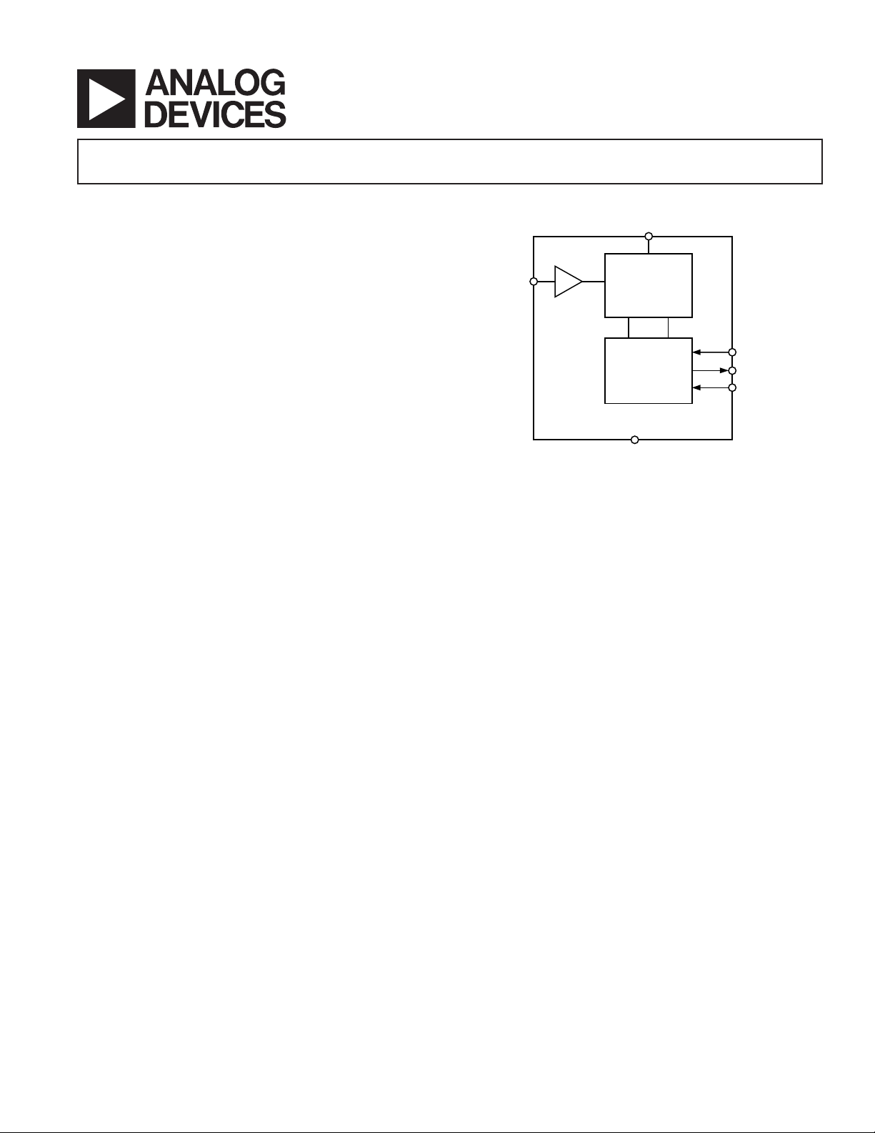
FUNCTIONAL BLOCK DIAGRAM
V
DD
V
T/H
IN
AD7476/AD7477/AD7478
8-/10-/12-BIT
SUCCESSIVE-
APPROXIMATION
ADC
CONTROL
LOGIC
GND
SCLK
SDATA
CS
GENERAL DESCRIPTION
The AD7476/AD7477/AD7478 are, respectively, 12-bit, 10-bit,
and 8-bit, high speed, low power, successive-approximation
ADCs. The parts operate from a single 2.35 V to 5.25 V power
supply and feature throughput rates up to 1 MSPS. The parts
contain a low noise, wide bandwidth track-and-hold amplifier
that can handle input frequencies in excess of 6 MHz.
The conversion process and data acquisition are controlled
using CS and the serial clock, allowing the devices to interface
with microprocessors or DSPs. The input signal is sampled on
the falling edge of CS and the conversion is also initiated at this
point. There are no pipeline delays associated with the part.
The AD7476/AD7477/AD7478 use advanced design techniques
to achieve very low power dissipation at high throughput rates.
The reference for the part is taken internally from V
DD.
This
allows the widest dynamic input range to the ADC. Thus the
analog input range for the part is 0 V to V
. The conversion
DD
rate is determined by the SCLK.
*Protected by U.S.Patent No. 6,681,332.
REV. D
Information furnished by Analog Devices is believed to be accurate and
reliable. However, no responsibility is assumed by Analog Devices for its
use, nor for any infringements of patents or other rights of third parties that
may result from its use. No license is granted by implication or otherwise
under any patent or patent rights of Analog Devices. Trademarks and
registered trademarks are the property of their respective owners.
PRODUCT HIGHLIGHTS
1. First 12-/10-/8-Bit ADCs in a SOT-23 Package.
2. High Throughput with Low Power Consumption.
3. Flexible Power/Serial Clock Speed Management.
The conversion rate is determined by the serial clock, allowing
the conversion time to be reduced through the serial clock
speed increase. This allows the average power consumption
to be reduced while not converting. The part also features a
shutdown mode to maximize power efficiency at lower
throughput rates. Current consumption is 1 µA maximum
when in shutdown.
4. Reference Derived from the Power Supply.
5. No Pipeline Delay.
The parts feature a standard successive-approximation ADC
with accurate control of the sampling instant via a CS input
and once-off conversion control.
One Technology Way, P.O. Box 9106, Norwood, MA 02062-9106, U.S.A.
Tel: 781/329-4700 www.analog.com
Fax: 781/326-8703 © 2004 Analog Devices, Inc. All rights reserved.

AD7476–SPECIFICATIONS
(A Version: VDD = 2.7 V to 5.25 V, f
noted; S and B Versions: VDD = 2.35 V to 5.25 V, f
1
unless otherwise noted; TA = T
MIN
to T
= 20 MHz, f
SCLK
, unless otherwise noted.)
MAX
= 1 MSPS, unless otherwise
SAMPLE
= 12 MHz, f
SCLK
SAMPLE
= 600 kSPS,
Parameter A Version
1, 2
B Version
1, 2
S Version
1, 2
Unit Test Conditions/Comments
DYNAMIC PERFORMANCE fIN = 100 kHz Sine Wave
Signal-to-(Noise + Distortion) (SINAD)369 70 69 dB min B Version, VDD = 2.4 V to 5.25 V
= 25°C
A
Signal-to-Noise Ratio (SNR)
Total Harmonic Distortion (THD)
Peak Harmonic or Spurious Noise (SFDR)
Intermodulation Distortion (IMD)
3
3
3
3
70 70 dB min T
71.5 dB typ
70 71 70 dB min B Version, VDD = 2.4 V to 5.25 V
72.5 dB typ
–80 –78 –78 dB typ
–82 –80 –80 dB typ
Second-Order Terms –78 –78 –78 dB typ fa = 103.5 kHz, fb = 113.5 kHz
Third-Order Terms –78 –78 –78 dB typ fa = 103.5 kHz, fb = 113.5 kHz
Aperture Delay 10 10 10 ns typ
Aperture Jitter 30 30 30 ps typ
Full Power Bandwidth 6.5 6.5 6.5 MHz typ @ 3 dB
DC ACCURACY S, B Versions, V
= (2.35 V to 3.6 V)4;
DD
A Version, VDD = (2.7 V to 3.6 V)
Resolution 12 12 12 Bits
Integral Nonlinearity
Differential Nonlinearity
Offset Error
Gain Error
3
3
3
3
± 1 ± 0.6 ± 0.6 LSB typ
± 0.75 ± 0.75 ± 0.75 LSB typ
± 1.5 ± 1.5 LSB max
–0.9/+1.5 –0.9/+1.5 LSB max Guaranteed No Missed Codes to 12 Bits
± 1.5 ± 2 LSB max
± 0.5 LSB typ
± 1.5 ± 2 LSB max
± 0.5 LSB typ
ANALOG INPUT
Input Voltage Ranges 0 to V
DD
0 to V
DD
0 to V
DD
V
DC Leakage Current ± 1 ± 1 ± 1 µA max
Input Capacitance 30 30 30 pF typ
LOGIC INPUTS
Input High Voltage, V
INH
2.4 2.4 2.4 V min
1.8 1.8 1.8 V min VDD = 2.35 V
Input Low Voltage, V
INL
0.4 0.4 0.4 V max VDD = 3 V
0.8 0.8 0.8 V max VDD = 5 V
Input Current, IIN, SCLK Pin ± 1 ± 1 ± 1 µA max Typically 10 nA, V
Input Current, IIN, CS Pin ± 1 ± 1 ± 1 µA typ
Input Capacitance, C
5
IN
10 10 10 pF max
= 0 V or V
IN
LOGIC OUTPUTS
Output High Voltage, V
Output Low Voltage, V
OH
OL
Floating-State Leakage Current ±10 ± 10 ±10 µA max
Floating-State Output Capacitance
VDD – 0.2 VDD – 0.2 VDD – 0.2 V min I
0.4 0.4 0.4 V max I
5
10 10 10 pF max
= 200 µA; VDD = 2.35 V to 5.25 V
SOURCE
= 200 µA
SINK
Output Coding Straight (Natural) Binary
CONVERSION RATE
Conversion Time 0.8 1.33 1.33 µs max 16 SCLK Cycles
Track-and-Hold Acquisition Time 500 500 500 ns max Full-Scale Step Input
350 400 400 ns max Sine Wave Input ≤100 kHz
Throughput Rate 1000 600 600 kSPS max See Serial Interface Section
POWER REQUIREMENTS
V
DD
I
DD
2.35/5.25 2.35/5.25 2.35/5.25 V min/max
Digital I/Ps = 0 V or V
DD
Normal Mode (Static) 222mA typ VDD = 4.75 V to 5.25 V. SCLK On or Off
111mA typ VDD = 2.35 V to 3.6 V. SCLK On or Off
Normal Mode (Operational) 3.5 3 3 mA max VDD = 4.75 V to 5.25 V; f
1.6 1.4 1.4 mA max VDD = 2.35 V to 3.6 V; f
SAMPLE
SAMPLE
Full Power-Down Mode 1 1 1 µA max SCLK Off
Power Dissipation
7
Normal Mode (Operational) 17.5 15 15 mW max VDD = 5 V; f
80 80 80 µA max SCLK On
4.8 4.2 4.2 mW max VDD = 3 V; f
SAMPLE
SAMPLE
= f
= f
SAMPLE
SAMPLE
Full Power-Down 5 5 5 µW max VDD = 5 V; SCLK Off
333µW max VDD = 3 V; SCLK Off
NOTES
1
Temperature ranges as follows: A, B Versions: –40°C to +85°C; S Version: –55°C to +125°C.
2
Operational from VDD = 2.0 V.
3
See Terminology section.
4
Maximum B, S version specifications apply as typical figures when VDD = 5.25 V.
5
Guaranteed by characterization.
6
A Version: f
7
See Power vs. Throughput Rate section.
MAX = 1 MSPS; B, S Versions: f
SAMPLE
Specifications subject to change without notice.
SAMPLE
DD
= f
= f
MAX
MAX
SAMPLE
SAMPLE
6
6
MAX
MAX
MAX = 600 kSPS.
6
6
REV. D–2–

AD7477–SPECIFICATIONS
1
(VDD = 2.7 V to 5.25 V, f
= 20 MHz, TA = T
SCLK
MIN
to T
, unless otherwise noted.)
MAX
Parameter A Version
1, 2
S Version
DYNAMIC PERFORMANCE f
1, 2
Unit Test Conditions/Comments
= 100 kHz Sine Wave, f
IN
SAMPLE
= 1 MSPS
Signal-to-(Noise + Distortion) (SINAD) 61 61 dB min
Total Harmonic Distortion (THD) –73 –73 dB max
Peak Harmonic or Spurious Noise (SFDR) –74 –74 dB max
Intermodulation Distortion (IMD)
Second-Order Terms –78 –78 dB typ fa = 103.5 kHz, fb = 113.5 kHz
Third-Order Terms –78 –78 dB typ fa = 103.5 kHz, fb = 113.5 kHz
Aperture Delay 10 10 ns typ
Aperture Jitter 30 30 ps typ
Full Power Bandwidth 6.5 6.5 MHz typ @ 3 dB
DC ACCURACY
Resolution 10 10 Bits
Integral Nonlinearity ± 1 ± 1 LSB max
Differential Nonlinearity ± 0.9 ± 0.9 LSB max Guaranteed No Missed Codes to 10 Bits
Offset Error ± 1 ± 1 LSB max
Gain Error ± 1 ± 1 LSB max
ANALOG INPUT
Input Voltage Ranges 0 to V
DD
0 to V
DD
V
DC Leakage Current ± 1 ± 1 µA max
Input Capacitance 30 30 pF typ
LOGIC INPUTS
Input High Voltage, V
Input Low Voltage, V
Input Current, I
Input Current, IIN, CS Pin ± 1 ± 1 µA typ
Input Capacitance, C
INH
INL
, SCLK Pin ± 1 ± 1 µA max Typically 10 nA, V
IN
4
IN
2.4 2.4 V min
0.8 0.8 V max VDD = 5 V
0.4 0.4 V max V
DD
= 3 V
10 10 pF max
= 0 V or V
IN
DD
LOGIC OUTPUTS
Output High Voltage, V
Output Low Voltage, V
Floating-State Leakage Current ±10 ±10 µA max
Floating-State Output Capacitance
OH
OL
4
VDD – 0.2 VDD – 0.2 V min I
0.4 0.4 V max I
10 10 pF max
= 200 µA; VDD = 2.7 V to 5.25 V
SOURCE
= 200 µA
SINK
Output Coding Straight (Natural) Binary
CONVERSION RATE
Conversion Time 800 800 ns max 16 SCLK Cycles with SCLK at 20 MHz
Track-and-Hold Acquisition Time 400 400 ns max
Throughput Rate 1 1 MSPS max See Serial Interface Section
POWER REQUIREMENTS
V
DD
I
DD
2.7/5.25 2.7/5.25 V min/max
Digital I/Ps = 0 V or V
DD
Normal Mode (Static) 2 2 mA typ VDD = 4.75 V to 5.25 V; SCLK On or Off
11mA typ V
Normal Mode (Operational) 3.5 3.5 mA max V
1.6 1.6 mA max V
= 2.7 V to 3.6 V; SCLK On or Off
DD
= 4.75 V to 5.25 V; f
DD
= 2.7 V to 3.6 V; f
DD
SAMPLE
SAMPLE
= 1 MSPS
= 1 MSPS
Full Power-Down Mode 1 1 µA max SCLK Off
Power Dissipation
5
Normal Mode (Operational) 17.5 17.5 mW max VDD = 5 V; f
80 80 µA max SCLK On
4.8 4.8 mW max V
= 3 V; f
DD
SAMPLE
SAMPLE
= 1 MSPS
= 1 MSPS
Full Power-Down 5 5 µW max VDD = 5 V; SCLK Off
NOTES
1
Temperature ranges as follows: A Version: –40°C to +85°C; S Version: –55°C to +125°C.
2
Operational from VDD = 2.0 V, with input high voltage, V
3
See Terminology section.
4
Guaranteed by characterization.
5
See Power vs. Throughput Rate section.
Specifications subject to change without notice.
= 1.8 V min.
INH
REV. D –3–

AD7476–SPECIFICATIONS
8
1
(VDD = 2.7 V to 5.25 V, f
= 20 MHz, TA = T
SCLK
MIN
to T
, unless otherwise noted.)
MAX
Parameter A Version
1, 2
S Version
DYNAMIC PERFORMANCE f
1, 2
Unit Test Conditions/Comments
= 100 kHz Sine Wave, f
IN
SAMPLE
= 1 MSPS
Signal-to-(Noise + Distortion) (SINAD) 49 49 dB min
Total Harmonic Distortion (THD) –65 –65 dB max
Peak Harmonic or Spurious Noise (SFDR) –65 –65 dB max
Intermodulation Distortion (IMD)
Second-Order Terms –68 –68 dB typ fa = 498.7 kHz, fb = 508.7 kHz
Third-Order Terms –68 –68 dB typ fa = 498.7 kHz, fb = 508.7 kHz
Aperture Delay 10 10 ns typ
Aperture Jitter 30 30 ps typ
Full Power Bandwidth 6.5 6.5 MHz typ @ 3 dB
DC ACCURACY
Resolution 8 8 Bits
Integral Nonlinearity ± 0.5 ±0.5 LSB max
Differential Nonlinearity ± 0.5 ± 0.5 LSB max Guaranteed No Missed Codes to Eight Bits
Offset Error ± 0.5 ±0.5 LSB max
Gain Error ± 0.5 ±0.5 LSB max
Total Unadjusted Error (TUE) ± 0.5 ±0.5 LSB max
ANALOG INPUT
Input Voltage Ranges 0 to V
DD
0 to V
DD
V
DC Leakage Current ± 1 ± 1 µA max
Input Capacitance 30 30 pF typ
LOGIC INPUTS
Input High Voltage, V
Input Low Voltage, V
Input Current, I
Input Current, IIN, CS Pin ± 1 ± 1 µA typ
Input Capacitance, C
INH
INL
, SCLK Pin ± 1 ± 1 µA max Typically 10 nA, V
IN
4
IN
2.4 2.4 V min
0.8 0.8 V max VDD = 5 V
0.4 0.4 V max V
DD
= 3 V
10 10 pF max
= 0 V or V
IN
DD
LOGIC OUTPUTS
Output High Voltage, V
Output Low Voltage, V
Floating-State Leakage Current ±10 ±10 µA max
Floating-State Output Capacitance
OH
OL
4
VDD – 0.2 VDD – 0.2 V min I
0.4 0.4 V max I
10 10 pF max
= 200 µA; VDD = 2.7 V to 5.25 V
SOURCE
= 200 µA
SINK
Output Coding Straight (Natural) Binary
CONVERSION RATE
Conversion Time 800 800 ns max 16 SCLK Cycles with SCLK at 20 MHz
Track-and-Hold Acquisition Time 400 400 ns max
Throughput Rate 1 1 MSPS max See Serial Interface Section
POWER REQUIREMENTS
V
DD
I
DD
2.7/5.25 2.7/5.25 V min/max
Digital I/Ps = 0 V or V
DD
Normal Mode (Static) 2 2 mA typ VDD = 4.75 V to 5.25 V; SCLK On or Off
11mA typ V
Normal Mode (Operational) 3.5 3.5 mA max V
1.6 1.6 mA max V
= 2.7 V to 3.6 V; SCLK On or Off
DD
= 4.75 V to 5.25 V; f
DD
= 2.7 V to 3.6 V; f
DD
SAMPLE
SAMPLE
= 1 MSPS
= 1 MSPS
Full Power-Down Mode 1 1 µA max SCLK Off
Power Dissipation
5
Normal Mode (Operational) 17.5 17.5 mW max VDD = 5 V; f
80 80 µA max SCLK On
4.8 4.8 mW max V
= 3 V; f
DD
SAMPLE
SAMPLE
= 1 MSPS
= 1 MSPS
Full Power-Down 5 5 µW max VDD = 5 V; SCLK Off
NOTES
1
Temperature ranges as follows: A Version: –40°C to +85°C; S Version: –55°C to +125°C.
2
Operational from VDD = 2.0 V, with input high voltage, V
3
See Terminology section.
4
Guaranteed by characterization.
5
See Power vs. Throughput Rate section.
Specifications subject to change without notice.
= 1.8 V min.
INH
REV. D–4–
AD7476/AD7477/AD7478
TIMING SPECIFICATIONS
Limit at T
AD7476/AD7477/AD7478
Parameter 3 V
4
f
SCLK
3
10 10 kHz min
1, 2
(VDD = 2.35 V to 5.25 V, TA = T
, T
MIN
MAX
3
5V
to T
MIN
, unless otherwise noted.)
MAX
Unit Description
20 20 MHz max A Version
12 12 MHz max B Version
t
CONVERT
t
QUIET
16 × t
SCLK
16 × t
SCLK
50 50 ns min Minimum Quiet Time Required between Bus Relinquish and
Start of Next Conversion
t
1
t
2
5
t
3
5
t
4
10 10 ns min Minimum CS Pulsewidth
10 10 ns min CS to SCLK Setup Time
20 20 ns max Delay from CS until SDATA Three-State Disabled
40 20 ns max Data Access Time after SCLK Falling Edge, A Version
70 20 ns max Data Access Time after SCLK Falling Edge, B Version
t
5
t
6
t
7
6
t
8
t
POWER-UP
NOTES
1
Guaranteed by characterization. All input signals are specified with tr = tf = 5 ns (10% to 90% of VDD) and timed from a voltage level of 1.6 V.
2
A Version timing specifications apply to the AD7477 S Version and AD7478 S Version; B Version timing specifications apply to the AD7476 S Version.
3
3 V specifications apply from VDD = 2.7 V to 3.6 V for A Version; 3 V specifications apply from VDD = 2.35 V to 3.6 V for B Version; 5 V specifications apply from
VDD = 4.75 V to 5.25 V.
4
Mark/Space ratio for the SCLK input is 40/60 to 60/40.
5
Measured with the load circuit of Figure 1 and defined as the time required for the output to cross 0.8 V or 2.0 V.
6
t8 is derived from the measured time taken by the data outputs to change 0.5 V when loaded with the circuit of Figure 1. The measured number is then extrapolated
to remove the effects of charging or discharging the 50 pF capacitor. This means that the time, t8, quoted in the Timing Specifications is the true bus relinquish time
of the part and is independent of the bus loading.
7
See Power-Up Time section.
Specifications subject to change without notice.
0.4 × t
0.4 × t
SCLK
SCLK
0.4 × t
0.4 × t
SCLK
SCLK
ns min SCLK Low Pulsewidth
ns min SCLK High Pulsewidth
10 10 ns min SCLK to Data Valid Hold Time
10 10 ns min SCLK Falling Edge to SDATA High Impedance
25 25 ns max SCLK Falling Edge to SDATA High Impedance
7
11µs typ Power-Up Time from Full Power-Down
REV. D
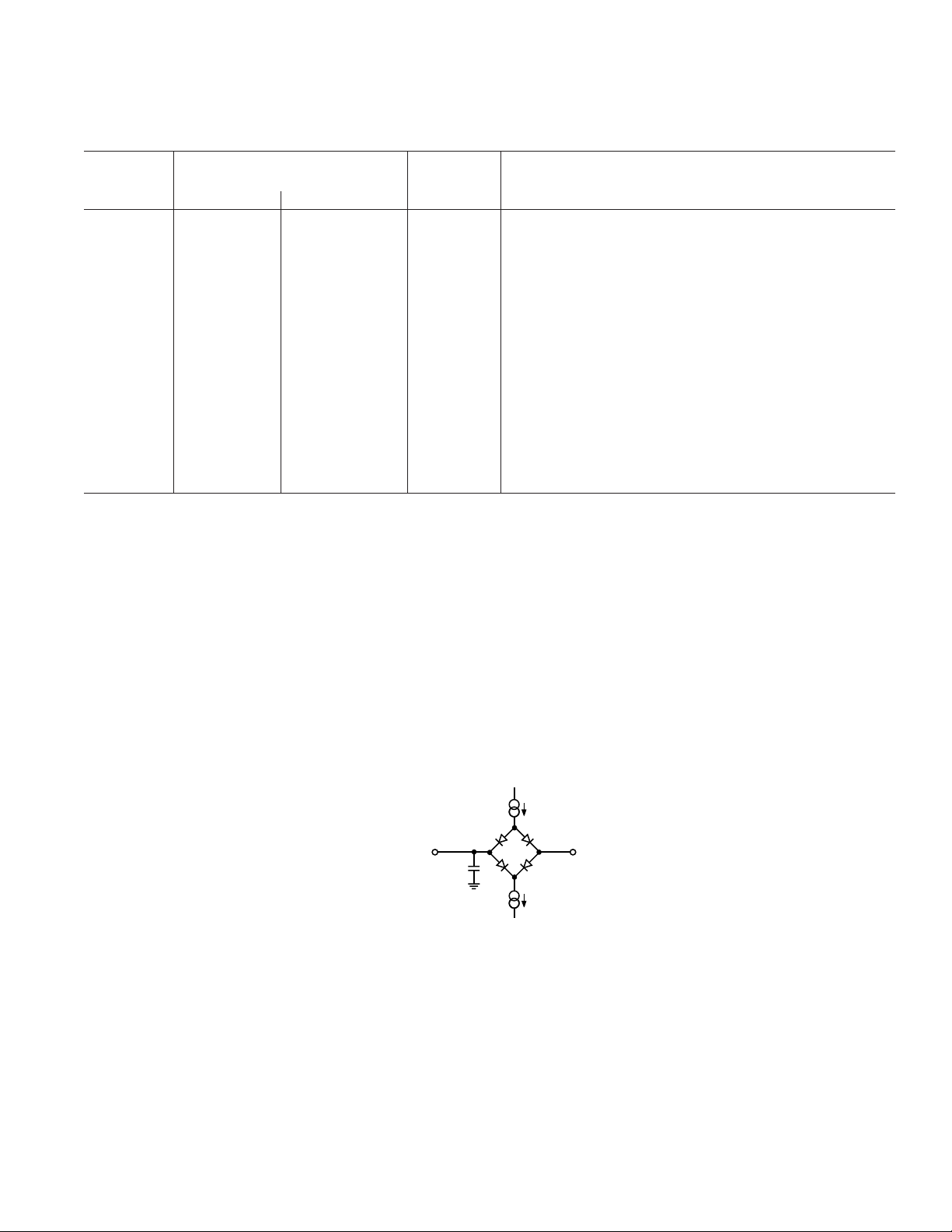
TO OUTPUT
PIN
50pF
200A
C
L
200A
I
OL
1.6V
I
OH
Figure 1. Load Circuit for Digital Output Timing
Specifications
–5–
AD7476/AD7477/AD7478
ABSOLUTE MAXIMUM RATINGS
(TA = 25°C, unless otherwise noted.)
1
VDD to GND . . . . . . . . . . . . . . . . . . . . . . . . . . . –0.3 V to +7 V
Analog Input Voltage to GND . . . . . . . . –0.3 V to V
+ 0.3 V
DD
Digital Input Voltage to GND . . . . . . . . . . . . . . –0.3 V to +7 V
Digital Output Voltage to GND . . . . . . –0.3 V to V
Input Current to Any Pin Except Supplies
2
. . . . . . . . ± 10 mA
+ 0.3 V
DD
Operating Temperature Range
Commercial (A, B Versions) . . . . . . . . . . . –40°C to +85°C
Military (S Version) . . . . . . . . . . . . . . . . . . –55°C to +125°C
Storage Temperature Range . . . . . . . . . . . . –65°C to +150°C
Junction Temperature . . . . . . . . . . . . . . . . . . . . . . . . . . 150°C
SOT-23 Package
Thermal Impedance . . . . . . . . . . . . . . . . . . . . . 230°C/W
θ
JA
θ
Thermal Impedance . . . . . . . . . . . . . . . . . . . . . . 92°C/W
JC
Lead Temperature, Soldering
Reflow (10 sec to 30 sec) . . . . . . . . . . . . . . . . 235 (0/+5)°C
Pb-Free Temperature Soldering
Reflow . . . . . . . . . . . . . . . . . . . . . . . . . . . . . . 255 (0/+5)°C
ESD . . . . . . . . . . . . . . . . . . . . . . . . . . . . . . . . . . . . . . . . 3.5 kV
NOTES
1
Stresses above those listed under Absolute Maximum Ratings may cause permanent damage to the device. This is a stress rating only; functional operation of the
device at these or any other conditions above those listed in the operational
sections of this specification is not implied. Exposure to absolute maximum rating
conditions for extended periods may affect device reliability.
2
Transient currents of up to 100 mA will not cause SCR latch-up.
ORDERING GUIDE
Model Range Error (LSB)
Temperature Linearity Package Branding
1
Option
2
Information
AD7476ART-500RL7 –40°C to +85°C ± 1 typ RT-6 CEA
AD7476ART-REEL –40°C to +85°C ± 1 typ RT-6 CEA
AD7476ART-REEL7 –40°C to +85°C ± 1 typ RT-6 CEA
AD7476ARTZ-500RL7
AD7476ARTZ-REEL
AD7476ARTZ-REEL7
3
3
3
–40°C to +85°C ± 1 typ RT-6 CEA
–40°C to +85°C ± 1 typ RT-6 CEA
–40°C to +85°C ± 1 typ RT-6 CEA
AD7476BRT-REEL –40°C to +85°C ± 1.5 max RT-6 CEB
AD7476BRT-REEL7 –40°C to +85°C ± 1.5 max RT-6 CEB
AD7476BRTZ-REEL
AD7476BRTZ-REEL7
3
3
–40°C to +85°C ± 1.5 max RT-6 CEB
–40°C to +85°C ± 1.5 max RT-6 CEB
AD7476SRT-500RL7 –55°C to +125°C ±1.5 max RT-6 CES
AD7476SRT-R2 –55°C to +125°C ± 1.5 max RT-6 CES
AD7476SRT-REEL –55°C to +125°C ±1.5 max RT-6 CES
AD7476SRT-REEL7 –55°C to +125°C ±1.5 max RT-6 CES
AD7476SRTZ-500RL7
AD7476SRTZ-R2
AD7476SRTZ-REEL
AD7476SRTZ-REEL7
3
3
3
3
–55°C to +125°C ±1.5 max RT-6 CES
–55°C to +125°C ±1.5 max RT-6 CES
–55°C to +125°C ±1.5 max RT-6 CES
–55°C to +125°C ±1.5 max RT-6 CES
AD7477ART-500RL7 –40°C to +85°C ± 1 max RT-6 CFA
AD7477ART-REEL –40°C to +85°C ± 1 max RT-6 CFA
AD7477ART-REEL7 –40°C to +85°C ± 1 max RT-6 CFA
AD7477SRT-500RL7 –55°C to +125°C ±1 max RT-6 CFS
AD7477SRT-R2 –55°C to +125°C ± 1 max RT-6 CFS
AD7477SRT-REEL –55°C to +125°C ±1 max RT-6 CFS
AD7477SRT-REEL7 –55°C to +125°C ±1 max RT-6 CFS
AD7478ART-500RL7 –40°C to +85°C ± 0.5 max RT-6 CJA
AD7478ART-REEL –40°C to +85°C ± 0.5 max RT-6 CJA
AD7478ART-REEL7 –40°C to +85°C ± 0.5 max RT-6 CJA
AD7478SRT-500RL7 –55°C to +125°C ±0.5 max RT-6 CJS
AD7478SRT-R2 –55°C to +125°C ± 0.5 max RT-6 CJS
AD7478SRT-REEL7 –55°C to +125°C ±0.5 max RT-6 CJS
EVAL-AD7476CB
EVAL-AD7477CB
EVAL-CONTROL BRD2
NOTES
1
Linearity Error here refers to integral linearity error.
2
RT = SOT-23.
3
Z = Pb free.
4
This can be used as a standalone evaluation board or in conjunction with the EVAL-CONTROL BOARD for evaluation/demonstration purposes.
5
This board is a complete unit allowing a PC to control and communicate with all Analog Devices evaluation boards ending in the CB designators. To order a complete
evaluation kit, you need to order the particular ADC evaluation board, e.g., EVAL-AD7476CB, the EVAL-CONTROL BRD2, and a 12 V ac transformer. See relevant
evaluation board application note for more information.
4
4
5
Evaluation Board
Evaluation Board
Control Board
CAUTION
ESD (electrostatic discharge) sensitive device. Electrostatic charges as high as 4000 V readily
accumulate on the human body and test equipment and can discharge without detection. Although the
AD7476/AD7477/AD7478 features proprietary ESD protection circuitry, permanent damage may
occur on devices subjected to high energy electrostatic discharges. Therefore, proper ESD precautions
are recommended to avoid performance degradation or loss of functionality.
REV. D–6–
 Loading...