1 MSPS,
a
FEATURES
Fast Throughput Rate: 1 MSPS
Specified for V
Low Power:
4.5 mW Max at 1 MSPS with 3 V Supplies
10.5 mW Max at 1 MSPS with 5 V Supplies
Wide Input Bandwidth:
68 dB SNR at 300 kHz Input Frequency
Flexible Power/Serial Clock Speed Management
No Pipeline Delays
High-Speed Serial Interface SPI™/QSPI™/
MICROWIRE™/DSP-Compatible
On-Board Reference 2.5 V (AD7495 Only)
Standby Mode: 1 A Max
8-Lead SOIC and SOIC Packages
APPLICATIONS
Battery-Powered Systems
Personal Digital Assistants
Medical Instruments
Mobile Communications
Instrumentation and Control Systems
Data Acquisition Systems
High-Speed Modems
Optical Sensors
GENERAL DESCRIPTION
The AD7475/AD7495 are 12-bit high-speed, low-power,
successive-approximation ADCs. The parts operate from a single
2.7 V to 5.25 V power supply and feature throughput rates up to
1 MSPS. The parts contain a low-noise, wide bandwidth track/hold
amplifier that can handle input frequencies in excess of 1 MHz.
The conversion process and data acquisition are controlled using
CS and the serial clock allowing the devices to interface with
microprocessors or DSPs. The input signal is sampled on the
falling edge of CS and conversion is also initiated at this point.
There are no pipelined delays associated with the part.
The AD7475/AD7495 use advanced design techniques to achieve
very low power dissipation at high throughput rates. With 3 V
supplies and 1 MSPS throughput rate, the AD7475 consumes just
1.5 mA, while the AD7495 consumes 2 mA. With 5 V supplies
and 1 MSPS, the current consumption is 2.1 mA for the AD7475
and 2.6 mA for the AD7495.
The analog input range for the part is 0 V to REF IN. The 2.5 V
reference for the AD7475 is applied externally to the REF IN pin
while the AD7495 has an on-board 2.5 V reference. The conversion time is determined by the SCLK frequency.
MICROWIRE is a trademark of National Semiconductor Corporation.
SPI and QSPI are trademarks of Motorola, Inc.
of 2.7 V to 5.25 V
DD
12-Bit ADCs
AD7475/AD7495
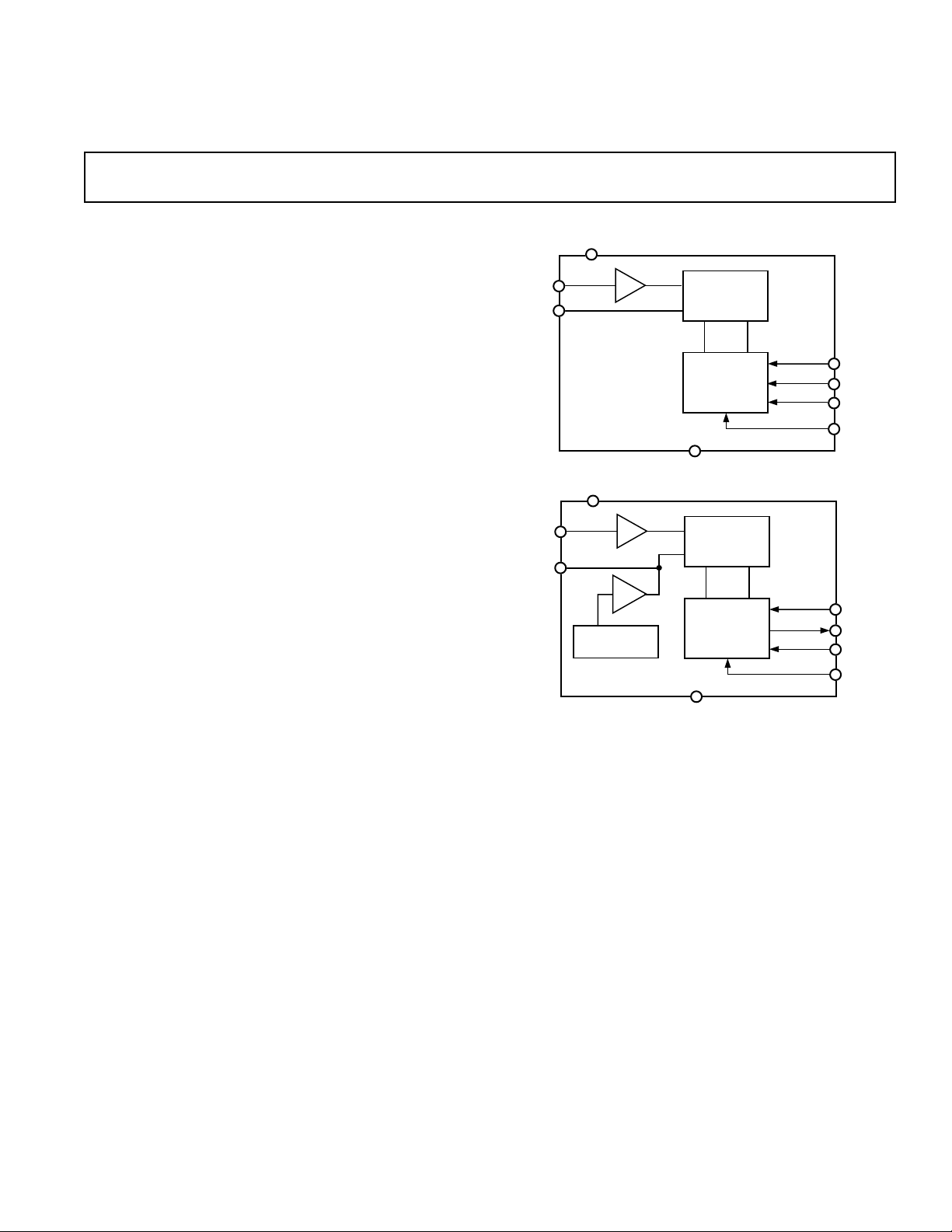
FUNCTIONAL BLOCK DIAGRAMS
V
DD
V
REF IN
V
REF OUT
IN
IN
T/H
AD7475
V
DD
T/H
BUF
2.5V
REFERENCE
AD7495
PRODUCT HIGHLIGHTS
1. High throughput with low power consumption. The
AD7475 offers 1 MSPS throughput rates with 4.5 mW
power consumption.
2. Single-supply operation with V
AD7495 operate from a single 2.7 V to 5.25 V supply. The
V
function allows the serial interface to connect directly
DRIVE
to either 3 V or 5 V processor systems independent of V
3. Flexible power/serial clock speed management. The conversion rate is determined by the serial clock, allowing the
conversion time to be reduced through the serial clock speed
increase. The part also features shutdown modes to maximize
power efficiency at lower throughput rates. This allows the
average power consumption to be reduced while not converting. Power consumption is 1 µA when in full shutdown.
4. No pipeline delay. The part features a standard successiveapproximation ADC with accurate control of the sampling
instant via a CS input and once off conversion control.
12-BIT
SUCCESSIVE
APPROXIMATION
ADC
CONTROL
LOGIC
GND
12-BIT
SUCCESSIVE
APPROXIMATION
ADC
CONTROL
LOGIC
GND
function. The AD7475/
DRIVE
SCLK
SDATA
CS
V
DRIVE
SCLK
SDATA
CS
V
DRIVE
DD
.
REV. A
Information furnished by Analog Devices is believed to be accurate and
reliable. However, no responsibility is assumed by Analog Devices for its
use, nor for any infringements of patents or other rights of third parties that
may result from its use. No license is granted by implication or otherwise
under any patent or patent rights of Analog Devices.
One Technology Way, P.O. Box 9106, Norwood, MA 02062-9106, U.S.A.
Tel: 781/329-4700 www.analog.com
Fax: 781/326-8703 © Analog Devices, Inc., 2001
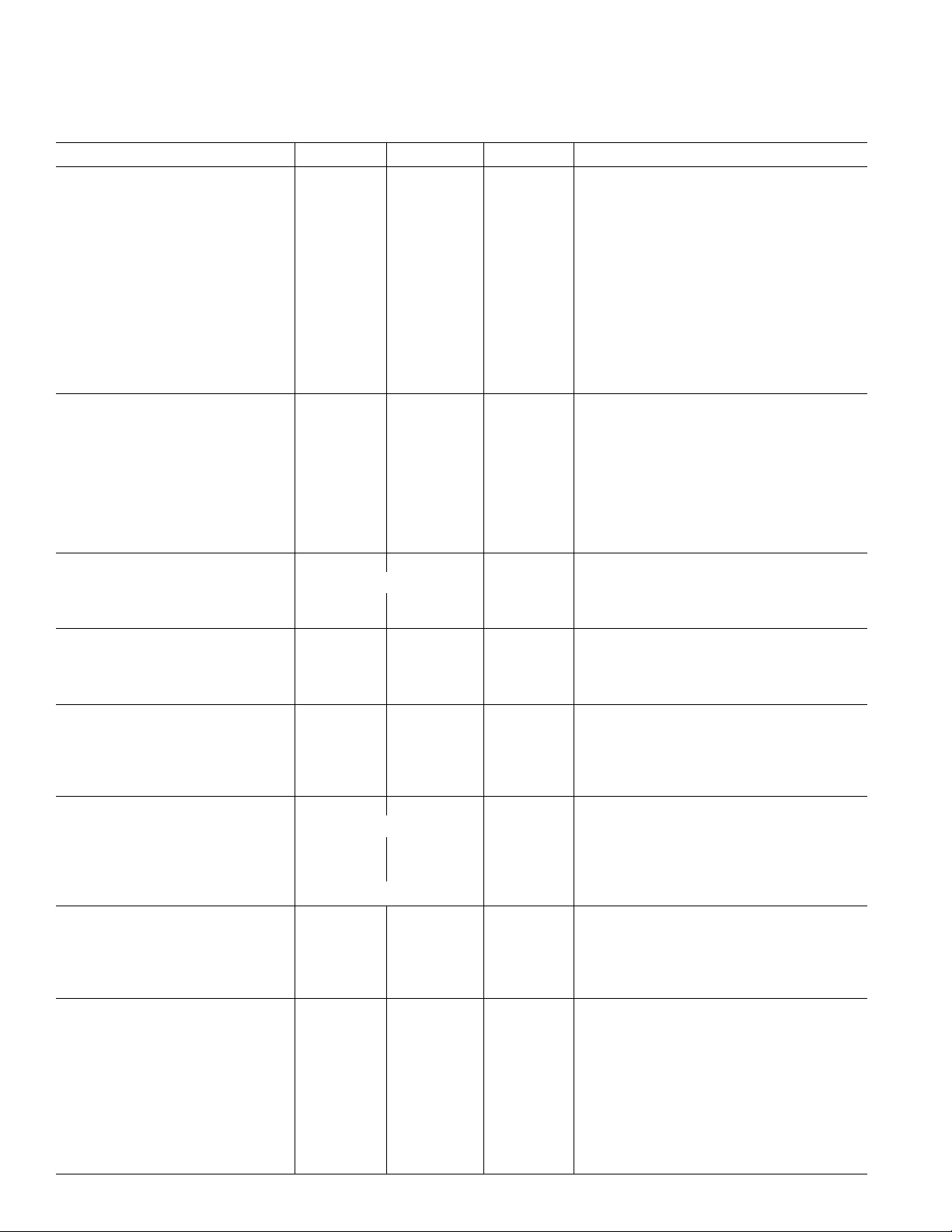
AD7475/AD7495–SPECIFICATIONS
1
(VDD = 2.7 V to 5.25 V, V
1
AD7475–SPECIFICATIONS
noted; TA = T
MIN
to T
Parameter A Version1B Version1Unit Test Conditions/Comments
DYNAMIC PERFORMANCE
Signal to Noise + Distortion Ratio 68 68 dB min f
(SINAD)
Total Harmonic Distortion (THD) –75 –75 dB max f
Peak Harmonic or Spurious Noise –76 –76 dB max f
(SFDR)
Intermodulation Distortion (IMD)
Second Order Terms –78 –78 dB typ
Third Order Terms –78 –78 dB typ
Aperture Delay 10 10 ns typ
Aperture Jitter 50 50 ps typ
Full Power Bandwidth 8.3 8.3 MHz typ @ 3 dB
Full Power Bandwidth 1.3 1.3 MHz typ @ 0.1 dB
DC ACCURACY
Resolution 12 12 Bits
Integral Nonlinearity ± 1.5 ± 1 LSB max @ 5 V (typ @ 3 V)
± 0.5 ± 0.5 LSB typ @ 25°C
Differential Nonlinearity +1.5/–0.9 +1.5/–0.9 LSB max @ 5 V Guaranteed No Missed Codes to 12 Bits
± 0.5 ± 0.5 LSB typ @ 25°C
Offset Error ± 8 ± 8 LSB max Typically ± 2.5 LSB
Gain Error ± 3 ± 3LSB max
ANALOG INPUT
Input Voltage Ranges 0 to REF IN Volts
DC Leakage Current ± 1 ± 1 µA max
Input Capacitance 20 20 pF typ
REFERENCE INPUT
REF IN Input Voltage Range 2.5 2.5 Volts ± 1% for Specified Performance
DC Leakage Current ± 1 ± 1 µA max
Input Capacitance 20 20 pF typ
LOGIC INPUTS
Input High Voltage, V
Input Low Voltage, V
Input Current, I
Input Capacitance, C
INL
IN
IN
INH
2
V
– 1 V
DRIVE
DRIVE
0.4 0.4 V max
± 1 ± 1 µA max Typically 10 nA, VIN = 0 V or V
10 10 pF max
LOGIC OUTPUTS
Output High Voltage, V
Output Low Voltage, V
Floating-State Leakage Current ± 10 ± 10 µA max
Floating-State Output Capacitance
OL
OH
0.4 0.4 V max I
2
10 10 pF max
V
– 0.2 V min I
DRIVE
Output Coding Straight (Natural) Binary
CONVERSION RATE
Conversion Time 800 800 ns max 16 SCLK Cycles with SCLK at 20 MHz
Track/Hold Acquisition Time 300 300 ns max Sine Wave Input
325 325 ns max Full-Scale Step Input
Throughput Rate 1 1 MSPS max See Serial Interface Section
POWER REQUIREMENTS
V
DD
V
DRIVE
I
DD
3
2.7/5.25 2.7/5.25 V min/max
2.7/5.25 2.7/5.25 V min/max
Normal Mode (Static) 750 750 A typ VDD = 2.7 V to 5.25 V. SCLK On or Off
Normal Mode (Operational) 2.1 2.1 mA max V
1.5 1.5 mA max V
Partial Power-Down Mode 450 450 µA typ f
Partial Power-Down Mode 100 100 µA max (Static)
Full Power-Down Mode 1 1 µA max SCLK On or Off
= 2.7 V to 5.25 V, REF IN = 2.5 V, f
DRIVE
, unless otherwise noted.)
MAX
– 1 V min
= 20 MHz unless otherwise
SCLK
= 300 kHz Sine Wave, f
IN
= 300 kHz Sine Wave, f
IN
= 300 kHz Sine Wave, f
IN
(typ @ 3 V)
= 200 µA; V
SOURCE
= 200 µA
SINK
DRIVE
Digital I/Ps = 0 V or V
= 4.75 V to 5.25 V. f
DD
= 2.7 V to 3.6 V. f
DD
= 100 kSPS
SAMPLE
= 1 MSPS
SAMPLE
= 1 MSPS
SAMPLE
= 1 MSPS
SAMPLE
DRIVE
= 2.7 V to 5.25 V
DRIVE
= 1 MSPS
SAMPLE
= 1 MSPS
SAMPLE
–2–
REV. A
AD7475/AD7495
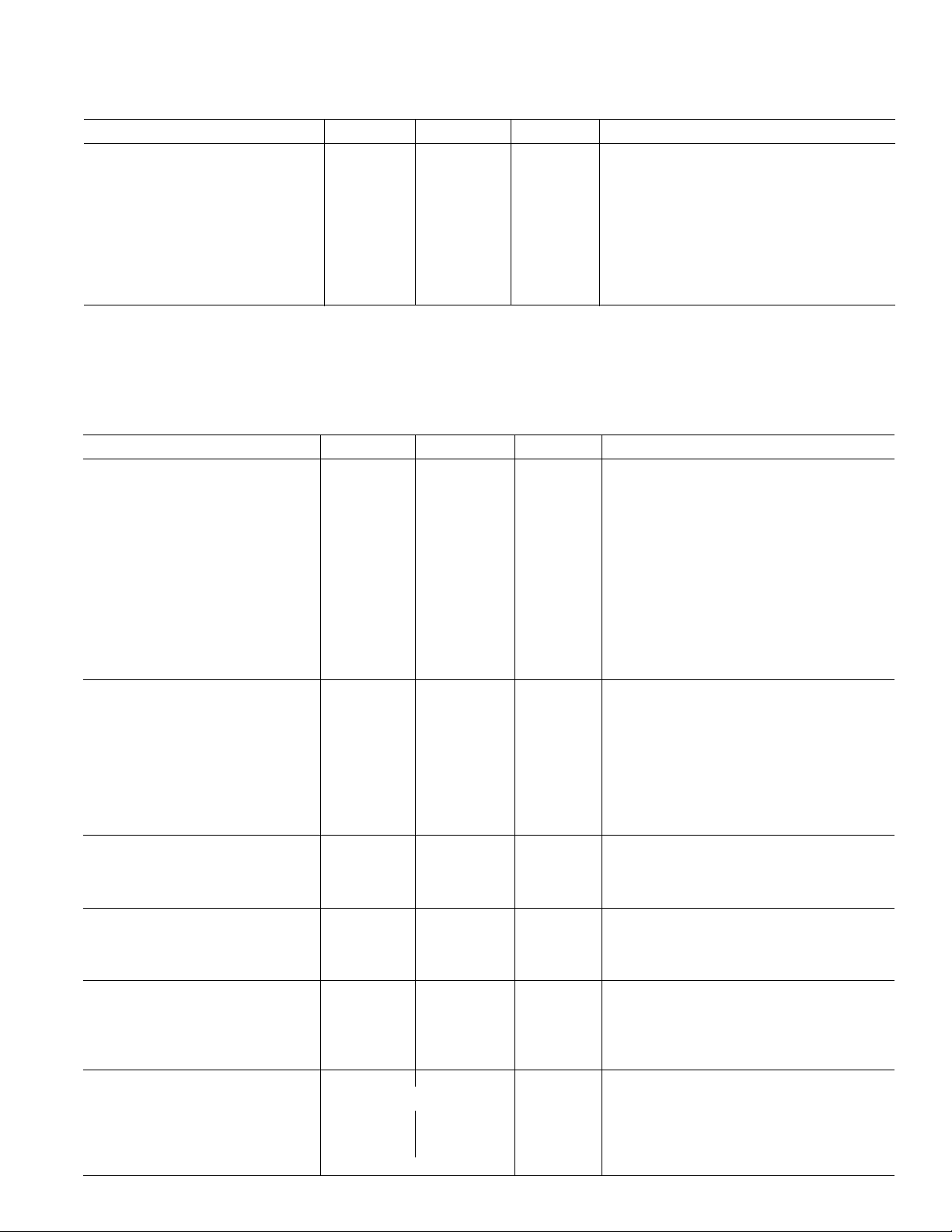
AD7475–SPECIFICATIONS (continued)
Parameter A Version1B Version1Unit Test Conditions/Comments
POWER REQUIREMENTS
(continued)
Power Dissipation
Normal Mode (Operational) 10.5 10.5 mW max VDD = 5 V. f
Partial Power-Down (Static) 500 500 W max V
Full Power-Down 5 5 W max V
NOTES
1
Temperature ranges as follows: A, B Versions: –40C to +85C.
2
Sample tested @ 25C to ensure compliance.
3
See Power Versus Throughput Rate section.
Specifications subject to change without notice.
3
= 1 MSPS
4.5 4.5 mW max V
300 300 W max V
= 3 V. f
DD
= 5 V
DD
= 3 V
DD
= 5 V
DD
SAMPLE
SAMPLE
= 1 MSPS
33W max VDD = 3 V
(VDD = 2.7 V to 5.25 V, V
AD7495–SPECIFICATIONS
1
T
, unless otherwise noted.)
MAX
Parameter A Version1B Version
= 2.7 V to 5.25 V, f
DRIVE
1
Unit Test Conditions/Comments
= 20 MHz unless otherwise noted; TA = T
SCLK
DYNAMIC PERFORMANCE
Signal to Noise + Distortion 68 68 dB min f
= 300 kHz Sine Wave, f
IN
SAMPLE
= 1 MSPS
(SINAD)
Total Harmonic Distortion (THD) –75 –75 dB max f
Peak Harmonic or Spurious Noise –76 –76 dB max f
= 300 kHz Sine Wave, f
IN
= 300 kHz Sine Wave, f
IN
SAMPLE
SAMPLE
= 1 MSPS
= 1 MSPS
(SFDR)
Intermodulation Distortion (IMD)
Second Order Terms –78 –78 dB typ
Third Order Terms –78 –78 dB typ
Aperture Delay 10 10 ns typ
Aperture Jitter 50 50 ps typ
Full Power Bandwidth 8.3 8.3 MHz typ @ 3 dB
Full Power Bandwidth 1.3 1.3 MHz typ @ 0.1 dB
DC ACCURACY
Resolution 12 12 Bits
Integral Nonlinearity ±1.5 ±1 LSB max @ 5 V (typ @ 3 V)
± 0.5 ±0.5 LSB typ @ 25°C
Differential Nonlinearity +1.5/–0.9 +1.5/–0.9 LSB max @ 5 V Guaranteed No Missed Codes to 12 Bits
(typ @ 3 V)
± 0.6 ±0.6 LSB typ @ 25°C
Offset Error ± 8 ± 8 LSB max Typically ±2.5 LSB
Gain Error ± 7 ± 7 LSB max Typically ±2.5 LSB
ANALOG INPUT
Input Voltage Ranges 0 to 2.5 0 to 2.5 Volts
DC Leakage Current ± 1 ± 1 µA max
Input Capacitance 20 20 pF typ
REFERENCE OUTPUT
REF OUT Output Voltage 2.4625/2.5375 2.4625/2.5375 V min/max
REF OUT Impedance 10 10 Ω typ
REF OUT Temperature Coefficient 50 50 ppm/C typ
LOGIC INPUTS
Input High Voltage, V
Input Low Voltage, V
Input Current, I
Input Capacitance, C
INL
IN
IN
INH
2
V
DRIVE
– 1 V
– 1 V min
DRIVE
0.4 0.4 V max
± 1 ± 1 µA max Typically 10 nA, VIN = 0 V or V
10 10 pF max
DRIVE
LOGIC OUTPUTS
Output High Voltage, V
Output Low Voltage, V
Floating-State Leakage Current ±10 ±10 µA max
Floating-State Output Capacitance
OH
OL
2
V
– 0.2 V min I
DRIVE
0.4 0.4 V max I
10 10 pF max
= 200 µA; VDD = 2.7 V to 5.25 V
SOURCE
= 200 µA
SINK
Output Coding Straight (Natural) Binary
MIN
to
REV. A
–3–
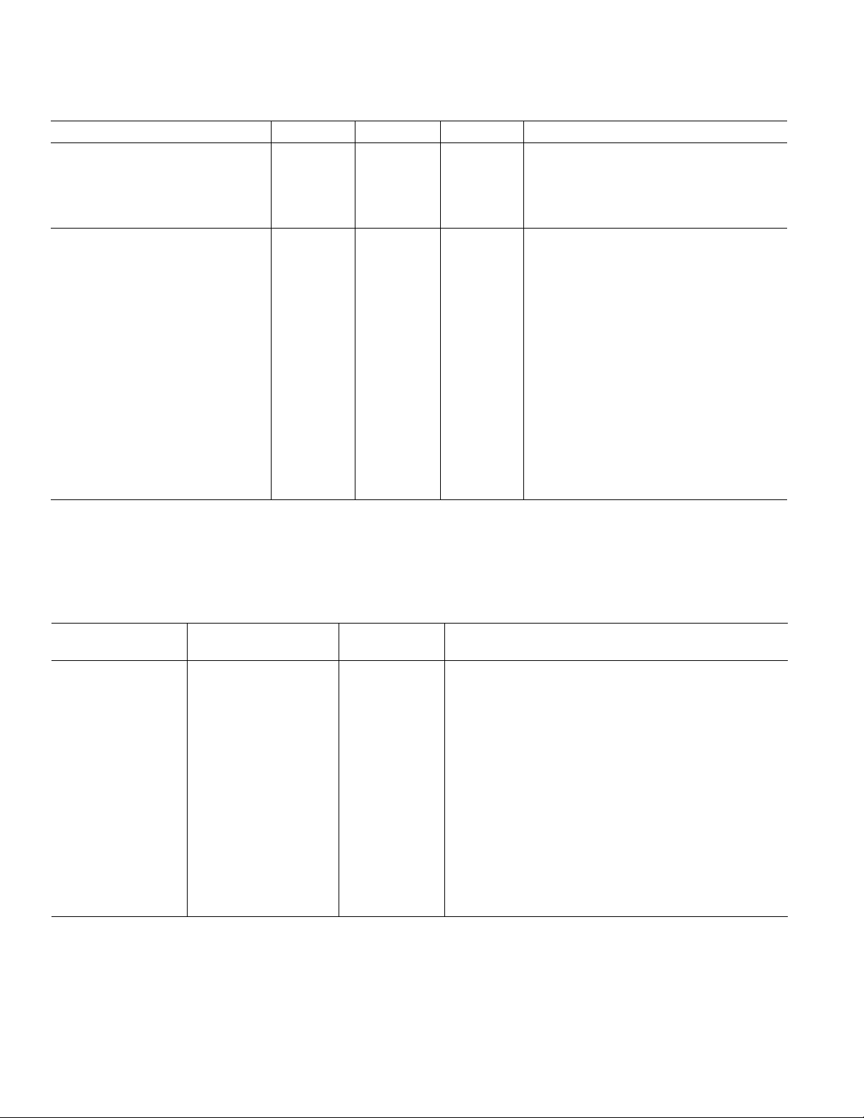
AD7475/AD7495–SPECIFICATIONS
1
AD7495–SPECIFICATIONS (continued)
Parameter A Version1B Version1Unit Test Conditions/Comments
CONVERSION RATE
Conversion Time 800 800 ns max 16 SCLK Cycles with SCLK at 20 MHz
Track/Hold Acquisition Time 300 300 ns max Sine Wave Input
325 325 ns max Full-Scale Step Input
Throughput Rate 1 1 MSPS max See Serial Interface Section
POWER REQUIREMENTS
V
DD
V
DRIVE
I
DD
Normal Mode (Static) 1 1 mA typ VDD = 2.7 V to 5.25 V. SCLK On or Off
Normal Mode (Operational) 2.6 2.6 mA max V
Partial Power-Down Mode 650 650 µA typ f
Partial Power-Down Mode 230 230 µA max (Static)
Full Power-Down Mode 1 1 µA max (Static) SCLK On or Off
Power Dissipation
3
Normal Mode (Operational) 13 13 mW max VDD = 5 V. f
Partial Power-Down (Static) 1.15 1.15 mW max V
Full Power-Down 5 5 µW max V
NOTES
1
Temperature ranges as follows: A, B Versions: –40C to +85C.
2
Sample tested @ 25C to ensure compliance.
3
See Power Versus Throughput Rate section.
Specifications subject to change without notice.
2.7/5.25 2.7/5.25 V min/max
2.7/5.25 2.7/5.25 V min/max
Digital I/Ps = 0 V or V
= 4.75 V to 5.25 V. f
DD
2 2 mA max V
6 6 mW max V
690 690 µW max V
= 2.7 V to 3.6 V. f
DD
= 100 kSPS
SAMPLE
= 3 V. f
DD
= 5 V
DD
= 3 V
DD
= 5 V
DD
33µW max VDD = 3 V
SAMPLE
SAMPLE
DRIVE
SAMPLE
SAMPLE
= 1 MSPS
= 1 MSPS
= 1 MSPS
= 1 MSPS
TIMING SPECIFICATIONS
Limit at T
(VDD = 2.7 V to 5.25 V, V
1
otherwise noted.)
, T
MIN
MAX
= 2.7 V to 5.25 V, REF IN = 2.5 V (AD7475); TA = T
DRIVE
MIN
to T
MAX
, unless
Parameter AD7475/AD7495 Unit Description
f
SCLK
2
10 kHz min
20 MHz max
t
CONVERT
t
QUIET
t
2
3
t
3
3
t
4
t
5
t
6
t
7
4
t
8
4
t
9
t
POWER-UP
16 × t
SCLK
800 ns max f
100 ns min Minimum Quiet Time Required between Conversions
10 ns min CS to SCLK Setup Time
22 ns max Delay from CS Until SDATA 3-State Disabled
40 ns max Data Access Time after SCLK Falling Edge
0.4 t
0.4 t
SCLK
SCLK
ns min SCLK Low Pulsewidth
ns min SCLK High Pulsewidth
10 ns min SCLK to Data Valid Hold Time
10 ns min SCLK Falling Edge to SDATA High Impedance
45 ns max SCLK Falling Edge to SDATA High Impedance
20 ns max CS Rising Edge to SDATA High Impedance
20 µs max Power-Up Time from Full Power-Down AD7475
t
SCLK
SCLK
= 1/f
SCLK
= 20 MHz
650 µs max Power-Up Time from Full Power-Down AD7495
NOTES
1
Sample tested at 25C to ensure compliance. All input signals are specified with tr = tf = 5 ns (10% to 90% of V
2
Mark/Space ratio for the SCLK input is 40/60 to 60/40.
3
Measured with the load circuit of Figure 3 and defined as the time required for the output to cross 0.8 V or 2.0 V.
4
t8 and t9 are derived from the measured time taken by the data outputs to change 0.5 V when loaded with the circuit of Figure 3. The measured number is then
extrapolated back to remove the effects of charging or discharging the 50 pF capacitor. This means that the times, t8 and t9, quoted in the timing characteristics are
the true bus relinquish time of the part and are independent of the bus loading.
Specifications subject to change without notice.
) and timed from a voltage level of 1.6 V.
DRIVE
–4–
REV. A
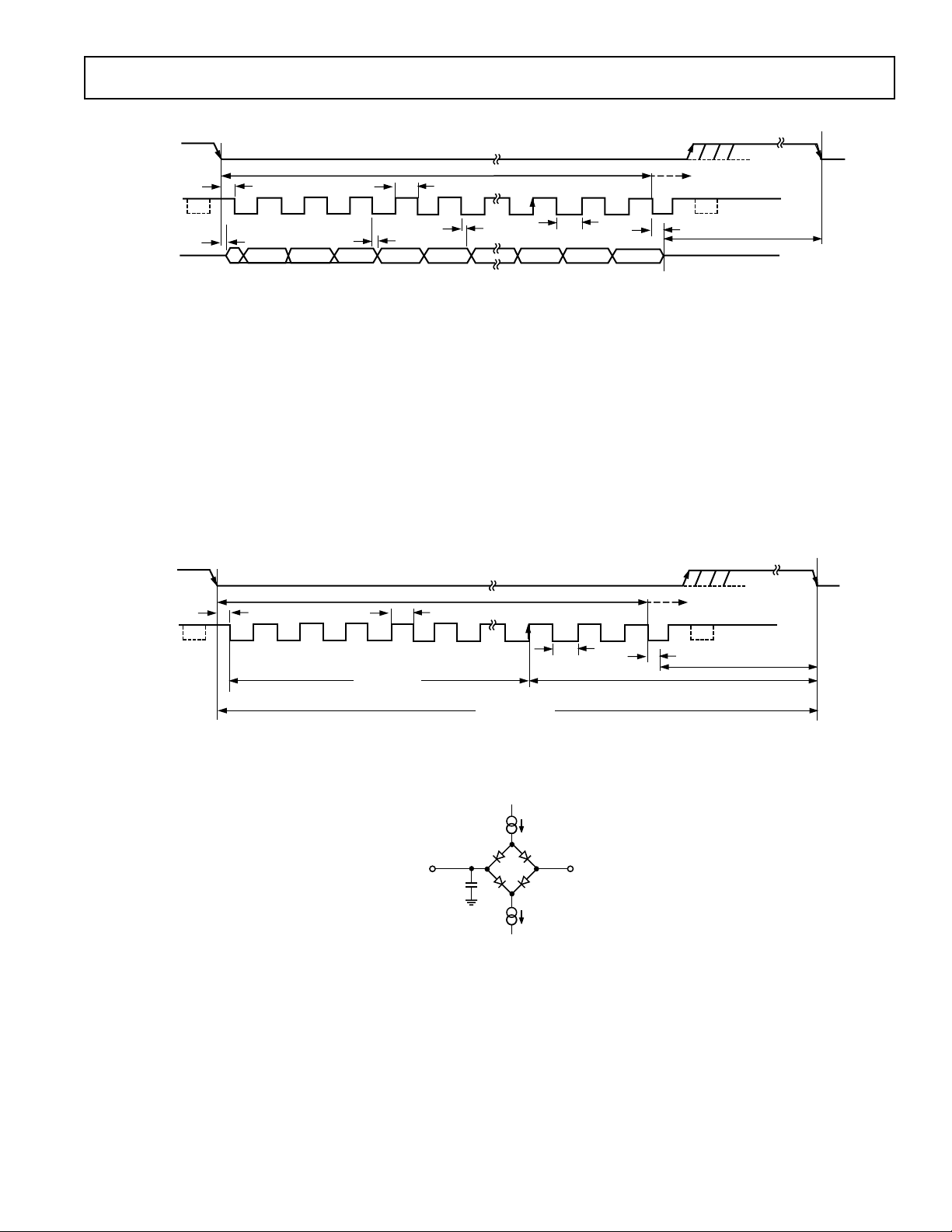
AD7475/AD7495
CS
t
SCLK
SDATA
THREE-STATE
2
1
t
3
00
FOUR LEADING ZEROS
2
0
34
0
Figure 1. Serial Interface Timing Diagram
Timing Example 1
Having f
time of t
leaves t
300 ns for t
+ t
QUIET
= 20 MHz and a throughput of 1 MSPS gives a cycle
SCLK
+ 12.5(1/f
2
to be 365 ns. This 365 ns satisfies the requirement of
ACQ
. From Figure 2, t
ACQ
SCLK
) + t
= 1 µs. With t2 = 10 ns min, this
ACQ
comprises of 2.5(1/f
ACQ
, where t8 = 45 ns. This allows a value of 195 ns for t
satisfying the minimum requirement of 100 ns.
Timing Example 2
Having f
cycle time of t
= 5 MHz and a throughput of 315 KSPS, gives a
SCLK
CS
SCLK
+ 12.5(1/f
2
t
2
10ns
SCLK
1
) + t
= 3.174 s.
ACQ
2
34
12.5 (1/f
t
CONVERT
t
6
5
t
7
t
4
DB11 DB10
) + t
SCLK
QUIET
t
CONVERT
t
6
5
)
SCLK
B
13
With t
14
DB2
= 10 ns min, this leaves t
2
satisfies the requirement of 300 ns for t
is comprised of 2.5(1/f
a value of 119 ns for t
of 100 ns. As in this example and with other slower clock values,
8
,
the signal may already be acquired before the conversion is
15
16
t
5
DB1
t
8
DB0
THREE-STATE
) + t8 + t
SCLK
satisfying the minimum requirement
QUIET
t
QUIET
to be 664 ns. This 664 ns
acq
. From Figure 2, t
ACQ
, t8 = 45 ns. This allows
QUIET
complete, but it is still necessary to leave 100 ns minimum
between conversions. In Example 2 the signal should be
t
QUIET
fully acquired at approximately Point C in Figure 2.
B
13
1/THROUGHPUT
C
14
t
15
16
5
t
8
45ns
t
ACQUISITION
t
QUIET
ACQ
REV. A
Figure 2. Serial Interface Timing Example
TO OUTPUT
PIN
50pF
200A
C
L
200A
I
OL
1.6V
I
OH
Figure 3. Load Circuit for Digital Output Timing Specifications
–5–
 Loading...