ANALOG DEVICES AD7470 Service Manual
1.75 MSPS, 4 mW
a
FEATURES
Specified for V
1.75 MSPS for AD7470 (10-Bit)
1.5 MSPS for AD7472 (12-Bit)
Low Power
AD7470: 3.34 mW Typ at 1.5 MSPS with 3 V Supplies
AD7472: 3.54 mW Typ at 1.2 MSPS with 3 V Supplies
Wide Input Bandwidth
70 dB Typ SNR at 500 kHz Input Frequency
Flexible Power/Throughput Rate Management
No Pipeline Delays
High Speed Parallel Interface
Sleep Mode: 50 nA Typ
24-Lead SOIC and TSSOP Packages
GENERAL DESCRIPTION
The AD7470/AD7472 are 10-bit/12-bit high speed, low power,
successive approximation ADCs. The parts operate from a single
2.7 V to 5.25 V power supply and feature throughput rates up to
1.5 MSPS for the 12-bit AD7472 and up to 1.75 MSPS for the
10-bit AD7470. The parts contain a low noise, wide bandwidth
track-and-hold amplifier that can handle input frequencies in
excess of 1 MHz.
The conversion process and data acquisition are controlled
using standard control inputs, allowing easy interfacing to
microprocessors or DSPs. The input signal is sampled on the
falling edge of CONVST, and conversion is also initiated at
this point. BUSY goes high at the start of conversion and
goes low 531.66 ns after falling edge of CONVST (AD7472
with a clock frequency of 26 MHz) to indicate that the conversion is complete. There are no pipeline delays associated
with the parts. The conversion result is accessed via standard
CS and RD signals over a high speed parallel interface.
The AD7470/AD7472 use advanced design techniques to
achieve very low power dissipation at high throughput rates. With
3 V supplies and 1.5 MSPS throughput rates, the AD7470
typically consumes, on average, just 1.1 mA. With 5 V supplies
and 1.75 MSPS, the average current consumption is typically
1.6 mA. The part also offers flexible power/throughput rate
management. Operating the AD7470 with 3 V supplies and
500 kSPS throughput reduces the current consumption to 713 µA.
At 5 V supplies and 500 kSPS, the part consumes 944 µA.
of 2.7 V to 5.25 V
DD
7.97 mW Typ at 1.75 MSPS with 5 V Supplies
8.7 mW Typ at 1.5 MSPS with 5 V Supplies
10-Bit/12-Bit Parallel ADCs
AD7470/AD7472
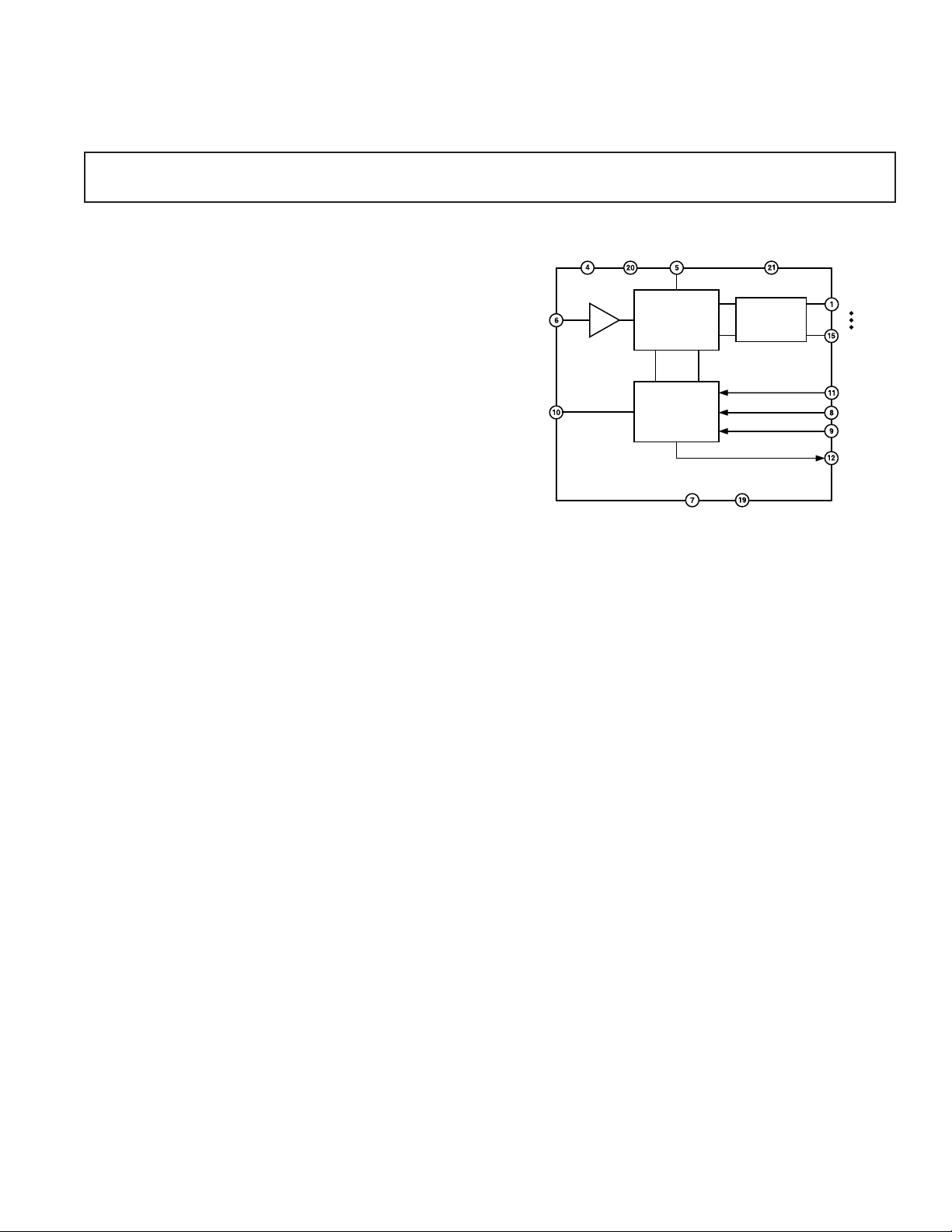
FUNCTIONAL BLOCK DIAGRAM
DV
V
CONVST
AV
DD
IN
T/H
AD7470/AD7472
AD7470 IS A 10-BIT PART WITH DB0 TO DB9 AS OUTPUTS.
AD7472 IS A 12-BIT PART WITH DB0 TO DB11 AS OUTPUTS.
REF IN
DD
10-/12-BIT
SUCCESSIVE
APPROXIMATION
ADC
CONTROL
LOGIC
AGND DGND
It is also possible to operate the parts in an auto sleep mode,
where the part wakes up to do a conversion and automatically
enters sleep mode at the end of conversion. This method allows
very low power dissipation numbers at lower throughput rates.
In this mode, the AD7472 can be operated with 3 V supplies at
100 kSPS, and consume an average current of just 124 µA. At
5 V supplies and 100 kSPS, the average current consumption is
171 µA.
The analog input range for the part is 0 V to REF IN. The 2.5 V
reference is applied externally to the REF IN pin. The conversion rate is determined by the externally-applied clock.
PRODUCT HIGHLIGHTS
1. High Throughput with Low Power Consumption. The
AD7470 offers 1.75 MSPS throughput and the AD7472
offers 1.5 MSPS throughput rates with 4 mW power
consumption.
2. Flexible Power/Throughput Rate Management. The conversion rate is determined by an externally-applied clock allowing the power to be reduced as the conversion rate is reduced.
The part also features an auto sleep mode to maximize power
efficiency at lower throughput rates.
3. No Pipeline Delay. The part features a standard successive
approximation ADC with accurate control of the sampling
instant via a CONVST input and once off conversion control.
V
DRIVE
OUTPUT
DRIVERS
DB9 (DB11)
DB0
CLK IN
CS
RD
BUSY
REV. B
Information furnished by Analog Devices is believed to be accurate and
reliable. However, no responsibility is assumed by Analog Devices for its
use, nor for any infringements of patents or other rights of third parties that
may result from its use. No license is granted by implication or otherwise
under any patent or patent rights of Analog Devices. Trademarks and
registered trademarks are the property of their respective owners.
One Technology Way, P.O. Box 9106, Norwood, MA 02062-9106, U.S.A.
Tel: 781/329-4700 www.analog.com
Fax: 781/326-8703 © 2003 Analog Devices, Inc. All rights reserved.

AD7470/AD7472
AD7470–SPECIFICATIONS
1
Parameter A Version
(VDD = 2.7 V to 5.25 V2, REF IN = 2.5 V, f
TA = T
1
MIN
3
to T
, unless otherwise noted.)
MAX
Unit Test Conditions/Comments
= 30 MHz @ 5 V and 24 MHz @ 3 V;
CLKIN
DYNAMIC PERFORMANCE 5 V 3 V fS = 1.75 MSPS @ 5 V, fS = 1.5 MSPS @ 3 V
Signal to Noise + Distortion (SINAD) 60 60 dB min fIN = 500 kHz Sine Wave
60 60 dB min fIN = 100 kHz Sine Wave
Signal-to-Noise Ratio (SNR) 60 60 dB min f
60 60 dB min fIN = 100 kHz Sine Wave
Total Harmonic Distortion (THD) –83 –83 dB typ f
–75 –75 dB max fIN = 100 kHz Sine Wave
Peak Harmonic or Spurious Noise (SFDR) –85 –85 dB typ f
–75 –75 dB max fIN = 100 kHz Sine Wave
= 500 kHz Sine Wave
IN
= 500 kHz Sine Wave
IN
= 500 kHz Sine Wave
IN
Intermodulation Distortion (IMD)
Second-Order Terms –79 –75 dB typ fIN = 500 kHz Sine Wave
–75 –75 dB max fIN = 100 kHz Sine Wave
Third-Order Terms –77 –75 dB typ fIN = 500 kHz Sine Wave
–75 –75 dB max fIN = 100 kHz Sine Wave
Aperture Delay 5 5 ns typ
Aperture Jitter 15 15 ps typ
Full Power Bandwidth 20 20 MHz typ @ 3 dB
DC ACCURACY fS = 1.75 MSPS @ 5 V; fS = 1.5 MSPS @ 3 V
Resolution 10 10 Bits
Integral Nonlinearity ± 1 ±1 LSB max
Differential Nonlinearity ± 0.9 ±0.9 LSB max Guaranteed No Missed Codes to 10 Bits
Offset Error ± 2.5 ±2.5 LSB max
Gain Error ± 1 ±1 LSB max
ANALOG INPUT
Input Voltage Ranges 0 to REF IN 0 to REF IN V
DC Leakage Current ±1 ±1 µA max
Input Capacitance 33 33 pF typ
REFERENCE INPUT
REF IN Input Voltage Range 2.5 2.5 V ±1% for Specified Performance
DC Leakage Current ±1 ±1 µA max
Input Capacitance 10/20 10/20 pF typ Track-and-Hold Mode
LOGIC INPUTS
Input High Voltage, V
Input Low Voltage, V
Input Current, I
Input Capacitance, C
IN
IN
INH
INL
4
2.4 2.4 V min
0.4 0.4 V max
± 1 ±1 µA max Typically 10 nA, VIN = 0 V or V
10 10 pF max
DD
LOGIC OUTPUTS
Output High Voltage, V
Output Low Voltage, V
Floating-State Leakage Current ± 10 ±10 µA max VDD = 2.7 V to 5.25 V
OH
OL
V
– 0.2 V
DRIVE
0.4 0.4 V max I
– 0.2 V min I
DRIVE
SOURCE
= 200 µA
SINK
= 200 µA
Floating-State Output Capacitance 10 10 pF max
Output Coding Straight (Natural) Binary
CONVERSION RATE
Conversion Time 12 12 CLK IN Cycles (max)
Track-and-Hold Acquisition Time 135 135 ns min
Throughput Rate 1.75 1.5 MSPS max Conversion Time + Acquisition Time
CLK IN of 30 MHz @ 5 V and 24 MHz @ 3 V
POWER REQUIREMENTS
V
DD
5
I
DD
Normal Mode 2.4 mA max VDD = 4.75 V to 5.25 V; fS = 1.75 MSPS; Typ 2 mA
+2.7/+5.25 V min/max
Digital Inputs = 0 V or DV
DD
Quiescent Current 900 µA max VDD = 4.75 V to 5.25 V; fS = 1.75 MSPS
Normal Mode 1.5 mA max VDD = 2.7 V to 3.3 V; fS = 1.5 MSPS; Typ 1.3 mA
Quiescent Current 800 µA max VDD = 2.7 V to 3.3 V; fS = 1.5 MSPS
Sleep Mode 1 µA max CLK IN = 0 V or DV
Power Dissipation
5
Digital Inputs = 0 V or DV
Normal Mode 12 mW max VDD = 5 V
DD
DD
4.5 mW max VDD = 3 V
Sleep Mode 5 µW max VDD = 5 V; CLK IN = 0 V or DV
3 µW max VDD = 3 V; CLK IN = 0 V or DV
NOTES
1
Temperature ranges as follows: A Version: –40°C to +85°C.
2
The AD7470 functionally works at 2.35 V. Typical specifications @ 25°C for SNR (100 kHz) = 59 dB; THD (100 kHz) = –84 dB; INL ± 0.8 LSB.
3
The AD7470 will typically maintain A-grade performance up to 125°C, with a reduced CLK of 20 MHz @ 5 V and 16 MHz @ 3 V. Typical sleep mode current @ 125°C is 700 nA.
4
Sample tested @ 25°C to ensure compliance.
5
See Power vs. Throughput Rate section.
Specifications subject to change without notice.
DD
DD
–2–
REV. B

AD7470/AD7472
1
AD7472–SPECIFICATIONS
Parameter A Version
DYNAMIC PERFORMANCE 5 V 3 V 5 V3 V
1
(VDD = 2.7 V to 5.25 V2, REF IN = 2.5 V, A and B Versions: f
20 MHz @ 3 V, TA = T
B Version
1
to T
MIN
, unless otherwise noted.)
MAX
Unit Test Conditions/Comments
fS = 1.5 MSPS @ 5 V, fS = 1.2 MSPS @ 3 V
Signal to Noise + Distortion (SINAD) 69 69 69 69 dB typ fIN = 500 kHz Sine Wave
Signal-to-Noise Ratio (SNR) 70 70 70 70 dB typ f
68 68 68 68 dB min f
68 68 68 68 dB min f
Total Harmonic Distortion (THD) –83 –78 –83 –78 dB typ fIN = 500 kHz Sine Wave
= 100 kHz Sine Wave
IN
= 500 kHz Sine Wave
IN
= 100 kHz Sine Wave
IN
–83 –84 –83 –84 dB typ fIN = 100 kHz Sine Wave
–75 –75 –75 –75 dB max fIN = 100 kHz Sine Wave
Peak Harmonic or Spurious Noise
(SFDR) –86 –81 –86 –81 dB typ fIN = 500 kHz Sine Wave
–86 –86 –86 –86 dB typ f
–76 –76 –76 –76 dB max f
Intermodulation Distortion (IMD)
= 100 kHz Sine Wave
IN
= 100 kHz Sine Wave
IN
Second-Order Terms –77 –77 –77 –77 dB typ fIN = 500 kHz Sine Wave
–86 –86 –86 –86 dB typ fIN = 100 kHz Sine Wave
Third-Order Terms –77 –77 –77 –77 dB typ fIN = 500 kHz Sine Wave
–86 –86 –86 –86 dB typ fIN = 100 kHz Sine Wave
Aperture Delay 5 5 5 5 ns typ
Aperture Jitter 15 15 15 15 ps typ
Full Power Bandwidth 20 20 20 20 MHz typ @ 3 dB
DC ACCURACY fS = 1.5 MSPS @ 5 V, fS = 1.2 MSPS @ 3 V
Resolution 12 12 12 12 Bits
Integral Nonlinearity ± 2 ± 2 ± 1 ± 1 LSB max Guaranteed No Missed Codes to 11 Bits
(A Version)
Differential Nonlinearity ± 1.8 ± 1.8 ± 0.9 ± 0.9 LSB max Guaranteed No Missed Codes to 12 Bits
(B Version)
Offset Error ± 10 ±10 ± 10 ± 10 LSB max
Gain Error ± 2 ± 2 ± 2 ± 2 LSB max
ANALOG INPUT
Input Voltage Ranges 0 to REF IN 0 to REF IN 0 to REF IN 0 to REF IN V
DC Leakage Current ±1 ± 1 ± 1 ± 1 µA max
Input Capacitance 33 33 33 33 pF typ
REFERENCE INPUT
REF IN Input Voltage Range 2.5 2.5 2.5 2.5 V ±1% for Specified Performance
DC Leakage Current ± 1 ± 1 ±1 ±1 µA max
Input Capacitance 10/20 10/20 10/20 10/20 pF typ Track-and-Hold Mode
LOGIC INPUTS
Input High Voltage, V
Input Low Voltage, V
Input Current, I
Input Capacitance, C
IN
IN
INH
INL
3
2.4 2.4 2.4 2.4 V min
0.4 0.4 0.4 0.4 V max
± 1 ± 1 ± 1 ± 1 µA max Typically 10 nA, VIN = 0 V or V
10 10 10 10 pF max
LOGIC OUTPUTS
Output High Voltage, V
Output Low Voltage, V
Floating-State Leakage Current ± 10 ±10 ± 10 ± 10 µA max VDD = 2.7 V to 5.25 V
OH
OL
V
– 0.2 V
DRIVE
0.4 0.4 0.4 0.4 V max I
DRIVE
– 0.2 V
DRIVE
– 0.2 V
– 0.2 V min I
DRIVE
SOURCE
= 200 µA
SINK
= 200 µA
Floating-State Output Capacitance 10 10 10 10 pF max
Output Coding Straight (Natural) Binary Straight (Natural) Binary
CONVERSION RATE
Conversion Time 14 14 14 14 CLK IN
Cycles (max)
Track-and-Hold Acquisition Time 135 135 135 135 ns min
Throughput Rate 1.5 1.2 1.5 1.2 MSPS max Conversion Time + Acquisition Time
POWER REQUIREMENTS
V
DD
4
I
DD
Normal Mode 2.4 2.4 mA max VDD = 4.75 V to 5.25 V; Typ 2 mA; fS = 1.5 MSPS
+2.7/+5.25 +2.7/+5.25 V min/max
Digital Inputs = 0 V or DV
Quiescent Current 900 900 µA max VDD = 4.75 V to 5.25 V; fS = 1.5 MSPS
Normal Mode 1.5 1.5 mA max VDD = 2.7 V to 3.3 V; Typ 1.3 mA; fS = 1.2 MSPS
Quiescent Current 800 800 µA max VDD = 2.7 V to 3.3 V; fS = 1.2 MSPS
Sleep Mode 1 1 µA max CLK IN = 0 V or DV
Power Dissipation
4
Digital Inputs = 0 V or DV
Normal Mode 12 12 mW max VDD = 5 V
4.5 4.5 mW max VDD = 3 V
Sleep Mode 5 5 µW max VDD = 5 V; CLK IN = 0 V or DV
33µW max VDD = 3 V; CLK IN = 0 V or DV
NOTES
1
Temperature ranges as follows: A and B Versions: –40°C to +85°C.
2
The AD7472 functionally works at 2.35 V. Typical specifications @ 25°C for SNR (100 kHz) = 68 dB; THD (100 kHz) = –84 dB; INL ± 0.8 LSB.
3
Sample tested @ 25°C to ensure compliance.
4
See Power vs. Throughput Rate section.
Specifications subject to change without notice.
= 26 MHz @ 5 V and
CLKIN
DD
DD
DD
DD
DD
DD
REV. B
–3–

AD7470/AD7472
AD7472–SPECIFICATIONS
1
Parameter Y Version
(VDD = 2.7 V to 5.25 V2, REF IN = 2.5 V,Y Version: f
14 MHz @ 3 V; TA = T
1
to T
MIN
, unless otherwise noted.)
MAX
Unit Test Conditions/Comments
= 20 MHz @ 5 V and
CLKIN
DYNAMIC PERFORMANCE 5 V 3 V fS = 1.2 MSPS @ 5 V, fS = 875 kSPS @ 3 V
Signal to Noise + Distortion (SINAD) 69 69 dB typ fIN = 500 kHz Sine Wave
68 68 dB min fIN = 100 kHz Sine Wave
Signal-to-Noise Ratio (SNR) 70 70 dB typ f
68 68 dB min fIN = 100 kHz Sine Wave
Total Harmonic Distortion (THD) –83 –78 dB typ f
–83 –84 dB typ fIN = 100 kHz Sine Wave
–75 –75 dB max f
Peak Harmonic or Spurious Noise (SFDR) –86 –81 dB typ fIN = 500 kHz Sine Wave
= 500 kHz Sine Wave
IN
= 500 kHz Sine Wave
IN
= 100 kHz Sine Wave
IN
–86 –86 dB typ fIN = 100 kHz Sine Wave
Intermodulation Distortion (IMD)
–76 –76 dB max f
= 100 kHz Sine Wave
IN
Second-Order Terms –77 –77 dB typ fIN = 500 kHz Sine Wave
–86 –86 dB typ fIN = 100 kHz Sine Wave
Third-Order Terms –77 –77 dB typ fIN = 500 kHz Sine Wave
–86 –86 dB typ fIN = 100 kHz Sine Wave
Aperture Delay 5 5 ns typ
Aperture Jitter 15 15 ps typ
Full Power Bandwidth 20 20 MHz typ @ 3 dB
DC ACCURACY fS = 1.2 MSPS @ 5 V; fS = 875 kSPS @ 3 V
Resolution 12 12 Bits
Integral Nonlinearity ± 2 ± 2 LSB max
Differential Nonlinearity ± 1.8 ±1.8 LSB max Guaranteed No Missed Codes to 11 Bits
Offset Error ± 10 ± 10 LSB max
Gain Error ± 2 ± 2 LSB max
ANALOG INPUT
Input Voltage Ranges 0 to REF IN 0 to REF IN V
DC Leakage Current ± 1 ±1 µA max
Input Capacitance 33 33 pF typ
REFERENCE INPUT
REF IN Input Voltage Range 2.5 2.5 V ±1% for Specified Performance
DC Leakage Current ± 1 ±1 µA max
Input Capacitance 10/20 10/20 pF typ Track-and-Hold Mode
LOGIC INPUTS
Input High Voltage, V
Input Low Voltage, V
Input Current, I
Input Capacitance, C
IN
IN
INH
INL
3
2.4 2.4 V min
0.4 0.4 V max
± 1 ± 1 µA max Typically 10 nA, VIN = 0 V or V
10 10 pF max
DD
LOGIC OUTPUTS
Output High Voltage, V
Output Low Voltage, V
Floating-State Leakage Current ± 10 ± 10 µA max VDD = 2.7 V to 5.25 V
OH
OL
V
– 0.2 V
DRIVE
0.4 0.4 V max I
– 0.2 V min I
DRIVE
SOURCE
= 200 µA
SINK
= 200 µA
Floating-State Output Capacitance 10 10 pF max
Output Coding Straight (Natural) Binary
CONVERSION RATE
Conversion Time 14 14 CLK IN Cycles (max)
Track-and-Hold Acquisition Time 140 140 ns min
Throughput Rate 1200 875 kSPS max Conversion Time + Acquisition Time
POWER REQUIREMENTS
V
DD
4
I
DD
Normal Mode 2.4 mA max VDD = 4.75 V to 5.25 V; fS = 1.2 MSPS; Typ 2 mA
+2.7/+5.25 V min/max
Digital Inputs = 0 V or DV
DD
Quiescent Current 900 µA max VDD = 4.75 V to 5.25 V; fS = 1.2 MSPS
Normal Mode 1.5 mA max VDD = 2.7 V to 3.3 V; fS = 875 kSPS; Typ 1.3 mA
Quiescent Current 800 µA max VDD = 2.7 V to 3.3 V; fS = 875 kSPS
Sleep Mode 2 µA max CLK IN = 0 V or DV
Power Dissipation
4
Digital Inputs = 0 V or DV
Normal Mode 12 mW max VDD = 5 V
DD
DD
4.5 mW max VDD = 3 V
Sleep Mode 10 µW max VDD = 5 V; CLK IN = 0 V or DV
6 µW max VDD = 3 V; CLK IN = 0 V or DV
NOTES
1
Temperature ranges as follows: Y Version: –40°C to +125°C.
2
The AD7472 functionally works at 2.35 V. Typical specifications @ 25°C for SNR (100 kHz) = 68 dB; THD (100 kHz) = –84 dB; INL ± 0.8 LSB.
3
Sample tested @ 25°C to ensure compliance.
4
See Power vs. Throughput Rate section.
Specifications subject to change without notice.
DD
DD
–4–
REV. B
AD7470/AD7472
1
TIMING SPECIFICATIONS
Limit at T
(VDD = 2.7 V to 5.25 V, REF IN = 2.5 V; TA = T
, T
MIN
MAX
Parameter AD7470 AD7472 Unit Description
2
f
CLK
10 10 kHz min
30 26 MHz max
t
CONVERT
t
WAKEUP
t
1
t
2
436.42 531.66 ns min t
11µs max Wake-Up Time
10 10 ns min CONVST Pulse Width
10 10 ns max V
15 ns max VDD = 5 V, Y Version
30 30 ns max V
35 ns max V
t
3
3
t
4
t
5
3
t
6
4
t
7
t
8
t
9
00ns max BUSY to CS Setup Time
00ns max CS to RD Setup Time
20 20 ns min RD Pulse Width
15 15 ns min Data Access Time After Falling Edge of RD
88ns max Bus Relinquish Time After Rising Edge of RD
00ns max CS to RD Hold Time
135 135 ns max A and B Versions
140 ns max Y Version
t
10
NOTES
1
Sample tested at 25°C to ensure compliance. All input signals are specified with tr = tf = 5 ns (10% to 90% of VDD) and timed from a voltage level of 1.6 V.
See Figure 1.
2
Mark/Space ratio for the CLK inputs is 40/60 to 60/40. First CLK pulse should be 10 ns min from falling edge of CONVST.
3
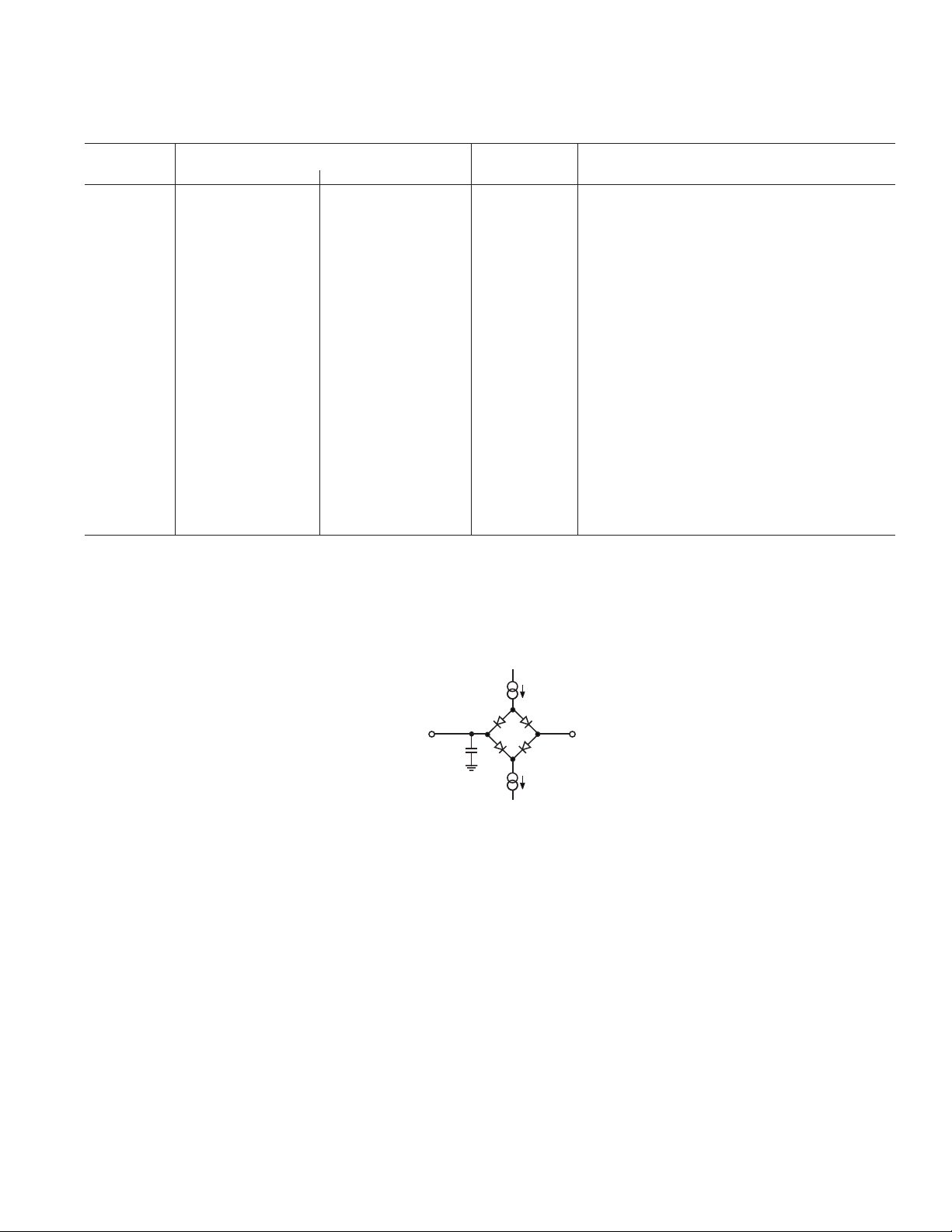
Measured with the load circuit of Figure 1 and defined as the time required for the output to cross 0.8 V or 2.0 V.
4
t7 is derived from the measured time taken by the data outputs to change 0.5 V when loaded with the circuit of Figure 1. The measured number is then extrapolated
back to remove the effects of charging or discharging the 50 pF capacitor. This means that the time, t
time of the part and is independent of the bus loading.
Specifications subject to change without notice.
100 100 ns min Quiet Time
200A
I
OL
to T
MIN
, unless otherwise noted.)
MAX
= 1/f
CLK
CLK IN
CONVST to BUSY Delay,
= 5 V, A and B Versions
DD
= 3 V, A and B Versions
DD
= 3 V, Y Version
DD
Acquisition Time
, quoted in the timing characteristics, is the true bus relinquish
7
TO OUTPUT
PIN
50pF
C
L
200A
I
OH
1.6V
Figure 1. Load Circuit for Digital Output Timing Specifications
REV. B
–5–
AD7470/AD7472
ABSOLUTE MAXIMUM RATINGS
(TA = 25°C unless otherwise noted.)
AV
to AGND/DGND . . . . . . . . . . . . . . . . . –0.3 V to +7 V
DD
to AGND/DGND . . . . . . . . . . . . . . . . . –0.3 V to +7 V
DV
DD
to AGND/DGND . . . . . . . . . . . . . . . . –0.3 V to +7 V
V
DRIVE
AV
to DVDD . . . . . . . . . . . . . . . . . . . . . . –0.3 V to +0.3 V
DD
to DVDD . . . . . . . . . . . . . . . –0.3 V to DVDD + 0.3 V
V
DRIVE
AGND to DGND . . . . . . . . . . . . . . . . . . . . –0.3 V to +0.3 V
Analog Input Voltage to AGND . . . . –0.3 V to AV
Digital Input Voltage to DGND . . . . –0.3 V to DVDD + 0.3 V
REF IN to AGND . . . . . . . . . . . . . . . –0.3 V to AV
Input Current to Any Pin Except Supplies
Operating Temperature Range
Commercial (A and B Versions) . . . . . . . . . –40°C to +85°C
Industrial (Y Version) . . . . . . . . . . . . . . . –40°C to +125°C
1
2
. . . . . . . . ± 10 mA
+ 0.3 V
DD
+ 0.3 V
DD
Junction Temperature . . . . . . . . . . . . . . . . . . . . . . . . . 150°C
Thermal Impedance . . . . . . . . . . . . . . . 75°C/W (SOIC)
θ
JA
. . . . . . . . . . . . . . . . . . . . . . . . . . . . . . . . .115°C/W (TSSOP)
Thermal Impedance . . . . . . . . . . . . . . . 25°C/W (SOIC)
θ
JC
. . . . . . . . . . . . . . . . . . . . . . . . . . . . . . . . 35°C/W (TSSOP)
Lead Temperature, Soldering
Vapor Phase (60 sec) . . . . . . . . . . . . . . . . . . . . . . . . 215°C
Infrared (15 sec) . . . . . . . . . . . . . . . . . . . . . . . . . . . . 220°C
ESD . . . . . . . . . . . . . . . . . . . . . . . . . . . . . . . . . . . . . . . .1.5 kV
NOTES
1
Stresses above those listed under Absolute Maximum Ratings may cause perma-
nent damage to the device. This is a stress rating only; functional operation of the
device at these or any other conditions above those listed in the operational
sections of this specification is not implied. Exposure to absolute maximum rating
conditions for extended periods may affect device reliability.
2
Transient currents of up to 100 mA will not cause SCR latch-up.
Storage Temperature Range . . . . . . . . . . . –65°C to +150°C
ORDERING GUIDE
Temperature Resolution Package Package
Model Range (Bits) Options
1
Description
AD7470ARU –40°C to +85°C10 RU-24 TSSOP
AD7470ARU-REEL –40°C to +85°C10 RU-24 TSSOP
AD7470ARU-REEL7 –40°C to +85°C10 RU-24 TSSOP
AD7472AR –40°C to +85°C12 R-24 SOIC
AD7472AR-REEL –40°C to +85°C12 R-24 SOIC
AD7472AR-REEL7 –40°C to +85°C12 R-24 SOIC
AD7472ARU –40°C to +85°C12 RU-24 TSSOP
AD7472ARU-REEL –40°C to +85°C12 RU-24 TSSOP
AD7472ARU-REEL7 –40°C to +85°C12 RU-24 TSSOP
AD7472BR –40°C to +85°C12 R-24 SOIC
AD7472BR-REEL –40°C to +85°C12 R-24 SOIC
AD7472BRU –40°C to +85°C12 RU-24 TSSOP
AD7472BRU-REEL –40°C to +85°C12 RU-24 TSSOP
AD7472BRU-REEL7 –40°C to +85°C12 RU-24 TSSOP
AD7472YR –40°C to +125°C12 R-24 SOIC
AD7472YR-REEL –40°C to +125°C12 R-24 SOIC
AD7472YRU –40°C to +125°C12 RU-24 TSSOP
AD7472YRU-REEL –40°C to +125°C12 RU-24 TSSOP
AD7472YRU-REEL7 –40°C to +125°C12 RU-24 TSSOP
EVAL-AD7470CB
EVAL-AD7472CB
EVAL CONTROL BRD2
NOTES
1
R = SOIC; RU = TSSOP.
2
This can be used as a standalone evaluation board or in conjunction with the EVAL-CONTROL BOARD for evaluation/demonstration purposes.
3
This board is a complete unit allowing a PC to control and communicate with all Analog Devices evaluation boards ending in the CB designators.
To order a complete evaluation kit, you need to order the specific ADC evaluation board, for example, EVAL-AD7472CB, the EVAL CONTROL
BRD2, and a 12 V ac transformer. See the relevant evaluation board application note for more information.
2
2
3
Evaluation Board
Evaluation Board
Controller Board
CAUTION
ESD (electrostatic discharge) sensitive device. Electrostatic charges as high as 4000 V readily
accumulate on the human body and test equipment and can discharge without detection.
Although the AD7470/AD7472 features proprietary ESD protection circuitry, permanent damage may occur on devices subjected to high energy electrostatic discharges. Therefore, proper
ESD precautions are recommended to avoid performance degradation or loss of functionality.
–6–
REV. B
 Loading...