

Low Power, Pseudo Differential, 100 kSPS
V
www.BDTIC.com/ADI
FEATURES
Specified for VDD of 2.7 V to 5.25 V
Low power:
DD
= 3 V
DD
= 5 V
0.9 mW max at 100 kSPS with V
3 mW max at 100 kSPS with V
Pseudo differential analog input
Wide input bandwidth:
70 dB SINAD at 30 kHz input frequency
Flexible power/serial clock speed management
No pipeline delays
High speed serial interface—SPI®-/QSPI™-/
MICROWIRE™-/DSP-compatible
Automatic power-down mode
8-lead SOT-23 package
APPLICATIONS
Transducer interface
Battery-powered systems
Data acquisition systems
Portable instrumentation
GENERAL DESCRIPTION
The AD7457 is a 12-bit, low power, successive approximation
(SAR) analog-to-digital converter that features a pseudo
differential analog input. This part operates from a single 2.7 V
to 5.25 V power supply and features throughput rates of up to
100 kSPS.
The part contains a low noise, wide bandwidth, differential
track-and-hold (T/H) amplifier that can handle input frequencies in excess of 1 MHz. The reference voltage for the AD7457 is
applied externally to the V
V
, depending on what suits the application.
DD
The conversion process and data acquisition are controlled
CS
using
and the serial clock, allowing the device to interface
with microprocessors or DSPs. The SAR architecture of this
part ensures that there are no pipeline delays.
The AD7457 uses advanced design techniques to achieve very
low power dissipation.
pin and can range from 100 mV to
REF
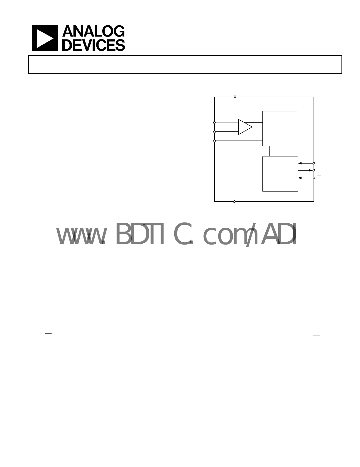
12-Bit ADC in an 8-Lead SOT-23
AD7457
FUNCTIONAL BLOCK DIAGRAM
V
DD
V
IN+
V
IN
–
REF
T/H
AD7457
GND
PRODUCT HIGHLIGHTS
1. Operation with 2.7 V to 5.25 V power supplies.
2. Low power consumption. With a 3 V supply, the AD7457
offers 0.9 mW maximum power consumption for a
100 kSPS throughput rate.
3. Pseudo differential analog input.
4. Flexible power/serial clock speed management. The
conversion rate is determined by the serial clock, allowing
the power to be reduced as the conversion time is reduced
through the serial clock speed increase. Automatic powerdown after conversion allows the average power consumption to be reduced.
5. Variable voltage reference input.
6. No pipeline delays.
7. Accurate control of the sampling instant via the
and once-off conversion control.
8. ENOB > 10 bits typically with 500 mV reference.
12-BIT
SUCCESSIVE
APPROXIMATION
ADC
CONTROL LOGIC
Figure 1.
CS
SCLK
SDATA
CS
input
03157-0-013
Rev. A
Information furnished by Analog Devices is believed to be accurate and reliable.
However, no responsibility is assumed by Analog Devices for its use, nor for any
infringements of patents or other rights of third parties that may result from its use.
Specifications subject to change without notice. No license is granted by implication
or otherwise under any patent or patent rights of Analog Devices. Trademarks and
registered trademarks are the property of their respective owners.
One Technology Way, P.O. Box 9106, Norwood, MA 02062-9106, U.S.A.
Tel: 781.329.4700 www.analog.com
Fax: 781.326.8703 © 2005 Analog Devices, Inc. All rights reserved.

AD7457
www.BDTIC.com/ADI
TABLE OF CONTENTS
Specifications..................................................................................... 3
Analog Input............................................................................... 12
Timing Specifications....................................................................... 5
Absolute Maximum Ratings............................................................ 6
ESD Caution.................................................................................. 6
Pin Configuration and Function Descriptions............................. 7
Typical Performance Characteristics ............................................. 8
Te r m in o l o g y .................................................................................... 10
Theory of Operation ...................................................................... 11
Circuit Information.................................................................... 11
Converter Operation.................................................................. 11
ADC Transfer Function............................................................. 11
Typical C o n necti on D i a g ram ................................................... 11
REVISION HISTORY
2/05—Rev. 0 to Rev. A
Changes to Table 3............................................................................ 6
Changes to Ordering Guide.......................................................... 17
Analog Input Structure.............................................................. 12
Digital Inputs .............................................................................. 13
Reference Section ....................................................................... 13
Serial Interface............................................................................ 13
Power Consumption .................................................................. 14
Microprocessor Interfacing....................................................... 14
Application Hints ........................................................................... 16
Grounding and Layout .............................................................. 16
Outline Dimensions....................................................................... 17
Ordering Guide .......................................................................... 17
10/03—Rev. 0: Initial Version
Rev. A | Page 2 of 20

AD7457
www.BDTIC.com/ADI
SPECIFICATIONS
VDD = 2.7 V to 5.25 V, f
Table 1.
Parameter Test Conditions/Comments B Version
DYNAMIC PERFORMANCE fIN = 30 kHz
Signal to Noise Ratio (SNR)
Signal to (Noise + Distortion) (SINAD)2 70 dB min
Total Harmonic Distortion (THD)2 −84 dB typ −75 dB max
Peak Harmonic or Spurious Noise2 −86 dB typ −75 dB max
Intermodulation Distortion (IMD)2 fa = 25 kHz; fb = 35 kHz
Second-Order Terms −80 dB typ
Third-Order Terms −80 dB typ
Aperture Delay2 5 ns typ
Aperture Jitter2 50 ps typ
Full-Power Bandwidth
@ −0.1 dB 2.5 MHz typ
DC ACCURACY
Resolution 12 Bits
Integral Nonlinearity (INL)2 ±1 LSB max
Differential Nonlinearity (DNL)2 Guaranteed no missed codes to 12 bits ±0.95 LSB max
Offset Error2 ±4.5 LSB max
Gain Error2 ±2 LSB max
ANALOG INPUT
Full-Scale Input Span
Absolute Input Voltage
V
IN+
4
V
IN−
V
DC Leakage Current ±1 µA max
Input Capacitance When in track/hold 30/10 pF typ
REFERENCE INPUT
V
Input Voltage
REF
DC Leakage Current ±1 µA max
V
Input Capacitance When in track/hold 10/30 pF typ
REF
LOGIC INPUTS
Input High Voltage, V
Input Low Voltage, V
Input Current, I
IN
Input Capacitance, C
LOGIC OUTPUTS
Output High Voltage, V
V
Output Low Voltage, V
Floating-State Leakage Current ±1 µA max
Floating-State Output Capacitance6 10 pF max
Output Coding Straight natural binary
CONVERSION RATE
Conversion Time 1.6 µs with a 10 MHz SCLK 16 SCLK cycles
Track-and-Hold Acquisition Time2 1 µs max
Throughput Rate See the Serial Interface section 100 kSPS max
= 10 MHz, fS = 100 kSPS, V
SCLK
2
2, 3
5
INH
INL
6
IN
OH
OL
= 2.5 V, TA = T
REF
MIN
to T
, unless otherwise noted.
MAX
1
Unit
71 dB min
@ −3 dB 20 MHz typ
V
− V
IN+
IN−
V
V
REF
REF
V
V
VDD = 2.7 V to 3.6 V −0.1 to +0.4 V
= 4.75 V to 5.25 V −0.1 to +1.5 V
DD
±1% tolerance for specified performance 2.5 V
2.4 V min
0.8 V max
Typically 10 nA, VIN = 0 V or V
DD
±1 µA max
10 pF max
VDD = 4.75 V to 5.25 V, I
= 2.7 V to 3.6 V, I
DD
I
= 200 µA 0.4 V max
SINK
= 200 µA 2.8 V min
SOURCE
= 200 µA 2.4 V min
SOURCE
Rev. A | Page 3 of 20
AD7457
www.BDTIC.com/ADI
Parameter Test Conditions/Comments B Version
1
Unit
POWER REQUIREMENTS
V
DD
7, 8
I
DD
During Conversion
6
V
2.7/5.25 V min/max
VDD = 4.75 V to 5.25 V 1.5 mA max
= 2.7 V to 3.6 V 1.2 mA max
DD
Normal Mode (Static) SCLK on or off 0.5 mA typ
Normal Mode (Operational) VDD = 4.75 V to 5.25 V 0.7 mA max
V
= 2.7 V to 3.6 V 0.33 mA max
DD
Power-Down SCLK on or off 1 µA max
Power Dissipation
Normal Mode (Operational) VDD = 5 V 3 mW max
V
= 3 V 0.9 mW max
DD
Power-Down VDD = 5 V; SCLK on or off 5 µW max
V
= 3 V; SCLK on or off 3 µW max
DD
1
Temperature range for B version: −40°C to +85°C.
2
See the section. Terminology
3
Analog inputs with slew rates exceeding 27 V/µs (full-scale input sine wave > 3.5 MHz) within the acquisition time may cause an incorrect result to be returned by the
converter.
4
A dc input is applied to V
5
The AD7457 is functional with a reference input range of 100 mV to VDD.
6
Guaranteed by characterization.
7
See the section. Power Consumption
8
Measured with a full-scale dc input.
to provide a pseudo ground for V
IN–
.
IN+
Rev. A | Page 4 of 20
AD7457
A
www.BDTIC.com/ADI
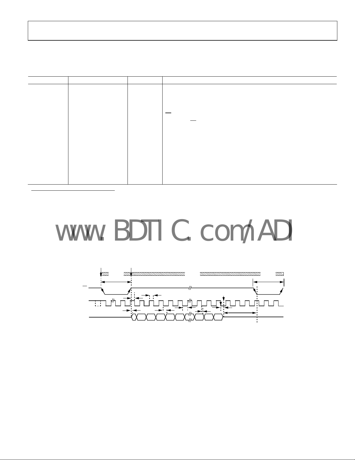
TIMING SPECIFICATIONS
VDD = 2.7 V to 5.25 V, f
Table 2.
Parameter Limit at T
2
f
SCLK
10 MHz max
t
CONVERT
1.6 µs max
t2 10 ns min
3
t
3
3
t
4
t5 0.4 t
t6 0.4 t
t7 10 ns min SCLK edge to data valid hold time
4
t
8
35 ns max SCLK falling edge to SDATA three-state enabled
5
t
POWER-UP
t
POWER-DOWN
1
The timing specifications are guaranteed by characterization. All input signals are specified with tr = tf = 5 ns (10% to 90% of VDD) and timed from a voltage level of
1.6 V. See and the Serial section. Figure 2 Interface
2
Mark/space ratio for the SCLK input is 40/60 to 60/40.
3
Measured with the load circuit of and defined as the time required for the output to cross 0.8 V or 2.4 V with VFigure 3
cross 0.4 V or 2.0 V for VDD = 3 V.
4
t8 is derived from the measured time taken by the data outputs to change 0.5 V when loaded with the circuit of The measured number is then extrapolated
back to remove the effects of charging or discharging the 25 pF capacitor. This means that the time, t8, quoted in the timing characteristics is the true bus relinquish
time of the part and is independent of the bus loading.
5
See the section. Power Consumption
= 10 MHz, fS = 100 kSPS, V
SCLK
, T
MIN
10 kHz min
16 × t
SCLK
20 ns max
40 ns max Data access time after SCLK falling edge
ns min SCLK high pulse width
SCLK
ns min SCLK low pulse width
SCLK
10 ns min SCLK falling edge to SDATA three-state enabled
1 µs max Power-up time from full power-down
7.4 µs min Minimum time spent in power-down
POWER
UP
CS
SCLK
SDAT
THREE-STATE
1
= 2.5 V, TA = T
REF
Unit Description
MAX
t
= 1/f
SCLK
CS
rising edge to SCLK falling edge setup time
Delay from CS rising edge until SDATA three-state disabled
CONVERT
START
TRACK TRACK
T
POWERUP
T
ACQUISITION
t
t
2
5
t
t
t
4
3
0 0 0 DB11 DB10 DB2 DB1 DB00
4 LEADING ZEROS
6
Figure 2. AD7457 Serial Interface Timing Diagram
SCLK
MIN
HOLD
t
7
to T
, unless otherwise noted.
MAX
DD
Figure 3.
AUTOMATIC
POWER DOWN
t
8
T
POWERDOWN
THREE-STATE
= 5 V, and the time required for the output to
T
POWERUP
T
ACQUISTION
03157-0-001
Rev. A | Page 5 of 20
AD7457
www.BDTIC.com/ADI
ABSOLUTE MAXIMUM RATINGS
TA = 25°C, unless otherwise noted.
Table 3.
Parameter Rating
VDD to GND −0.3 V to +7 V
V
to GND −0.3 V to VDD + 0.3 V
IN+
V
to GND −0.3 V to VDD + 0.3 V
IN–
Digital Input Voltage to GND −0.3 V to +7 V
Digital Output Voltage to GND −0.3 V to VDD + 0.3 V
V
to GND −0.3 V to VDD + 0.3 V
REF
Input Current
Operating Temperature Range
to Any Pin Except
Supplies1±10 mA
Commercial (B Version) −40°C to +85°C
Storage Temperature Range −65°C to +150°C
Junction Temperature 150°C
θJA Thermal Impedance 211.5°C/W (SOT-23)
θJC Thermal Impedance 91.99°C/W (SOT-23)
Lead Temperature, Soldering
Vapor Phase (60 sec) 215°C
Infrared (15 sec) 220°C
Pb-Free Temperature, Soldering
Reflow 260(+0)°C
1
Transient currents of up to 100 mA do not cause SCR latch-up.
Stresses above those listed under Absolute Maximum Ratings
may cause permanent damage to the device. This is a stress
rating only; functional operation of the device at these or any
other conditions above those listed in the operational sections
of this specification is not implied. Exposure to absolute
maximum rating conditions for extended periods may affect
device reliability.
Figure 3. Load Circuit for Digital Output Timing Specifications
OUTPUT
PIN
I
OL
1.6mA
TO
C
L
25pF
I
OH
200µA
1.6V
03157-0-012
ESD CAUTION
ESD (electrostatic discharge) sensitive device. Electrostatic charges as high as 4000 V readily accumulate on the
human body and test equipment and can discharge without detection. Although this product features
proprietary ESD protection circuitry, permanent damage may occur on devices subjected to high energy
electrostatic discharges. Therefore, proper ESD precautions are recommended to avoid performance
degradation or loss of functionality.
Rev. A | Page 6 of 20

AD7457
www.BDTIC.com/ADI
PIN CONFIGURATION AND FUNCTION DESCRIPTIONS
V
8
REF
V
7
IN+
6
V
–
IN
GND
5
03157-0-002
input. Connect to ground or to a dc offset to
IN+
Table 4. Pin Function Descriptions
Pin No. Mnemonic Description
1 VDD
Power Supply Input. VDD is 2.7 V to 5.25 V. This supply should be decoupled to GND with a 0.1 µF capacitor and a
10 µF tantalum capacitor.
2 SCLK
Serial Clock. Logic input. SCLK provides the serial clock for accessing data from the part. This clock input is also
used as the clock source for the conversion process.
3 SDATA
Serial Data. Logic output. The conversion result from the AD7457 is provided on this output as a serial data
stream. The bits are clocked out on the falling edge of the SCLK input. The data stream of the AD7457 consists of
four leading zeros followed by the 12 bits of conversion data that are provided MSB first. The output coding is
straight (natural) binary.
4
CS
Chip Select. This input provides the dual function of powering up the device and initiating a conversion on the
AD7457.
5 GND
Analog Ground. Ground reference point for all circuitry on the AD7457. All analog input signals and any external
reference signal should be referred to this GND voltage.
6 V
IN–
Inverting Input. This pin sets the ground reference point for the V
provide a pseudo ground.
7 V
8 V
Noninverting Analog Input.
IN+
REF
Reference Input for the AD7457. An external reference in the range 100 mV to VDD must be applied to this input.
The specified reference input is 2.5 V. This pin should be decoupled to GND with a capacitor of at least 0.33 µF.
V
1
DD
SCLK
2
AD7457
3
SDATA
Figure 4. 8-Lead SOT-23 Pin Configuration
CS
TOP VIEW
(Not to Scale)
4
Rev. A | Page 7 of 20
AD7457
www.BDTIC.com/ADI
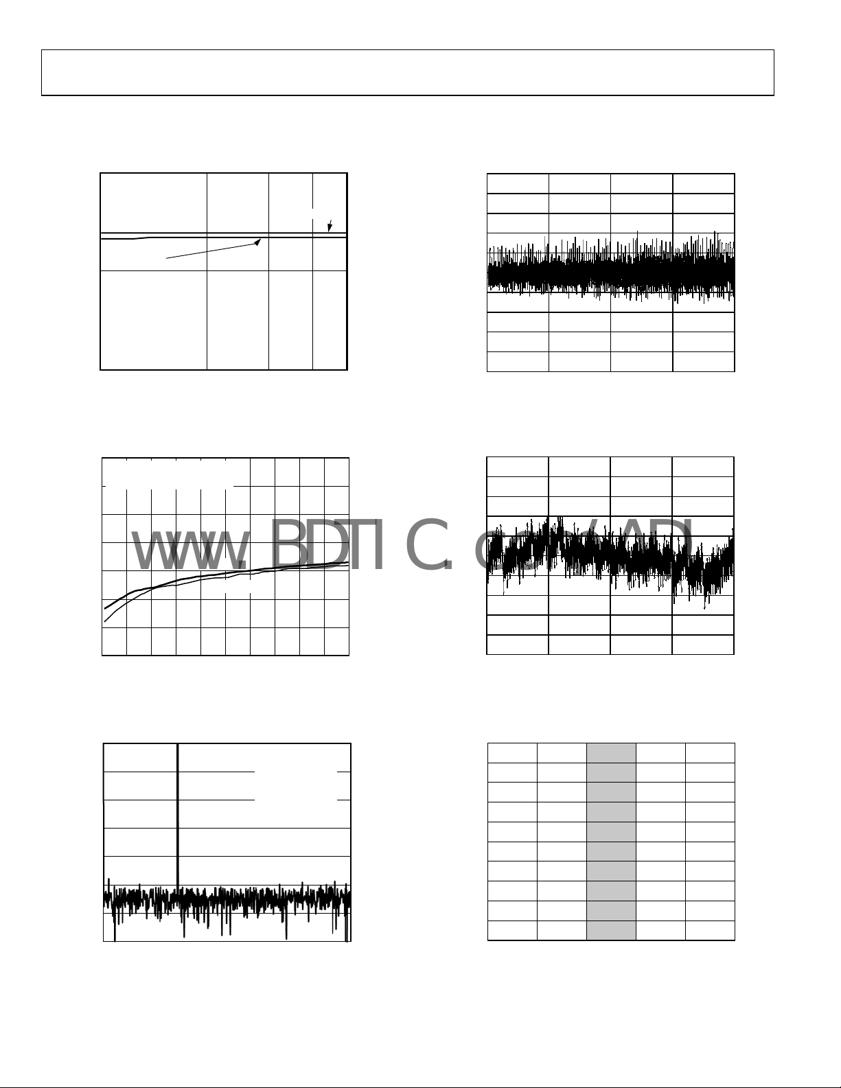
TYPICAL PERFORMANCE CHARACTERISTICS
TA = 25°C, fS = 100 kSPS, f
75
70
SINAD (dB)
65
Figure 5. SINAD vs. Analog Input Frequency for V
–20
–40
–60
–80
PSRR (dB)
–100
–120
–140
Figure 6. PSRR vs. Supply Ripple Frequency Without Supply Decoupling
–20
–40
–60
–80
SNR (dB)
–100
–120
–140
VDD = 3V
10
0
100mV p-p SINEWAVE ON V
NO DECOUPLING ON V
0 100 200 300 400 500
0
0 100
SUPPLY RIPPLE FREQUENCY (kHz)
Figure 7. Dynamic Performance for V
= 10 MHz, VDD = 2.7 V to 5.25 V, V
SCLK
VDD = 5V
20 50
FREQUENCY (kHz)
30 40
= 3 V and 5 V
DD
DD
DD
VDD= 3V
VDD= 5V
600 700 800
8192 POINT FFT
f
= 100kSPS
SAMPLE
f
= 30kHz
IN
SINAD = 71dB
THD = –82dB
SFDR = –83dB
30 50
FREQUENCY (kHz)
= 5 V
DD
900 1000
03157-0-014
03157-0-015
03157-0-016
= 2.5 V, unless otherwise noted.
REF
1.0
0.8
0.6
0.4
0.2
0
–0.2
DNL ERROR (LSB)
–0.4
–0.6
–0.8
–1.0
0 1024 30722048 4096
Figure 8. Typical DNL for the AD7457 for V
1.0
0.8
0.6
0.4
0.2
0
–0.2
INL ERROR (LSB)
–0.4
–0.6
–0.8
–1.0
0 1024 30722048 4096
Figure 9. Typical INL for the AD7457 for V
CODE
CODE
DD
DD
= 5 V
= 5 V
10,000
9,000
8,000
7,000
6,000
5,000
COUNTS
4,000
3,000
2,000
1,000
0
2046 2047 2048 2049 2050 2051
27 CODES 24 CODES
9949
CODES
CODES
Figure 10. Histogram of 10,000 Conversions of a DC Input
03157-0-017
03157-0-018
03157-0-019
Rev. A | Page 8 of 20

AD7457
www.BDTIC.com/ADI
4.0
3.5
3.0
2.5
2.0
1.5
REF
REF
(V)
(V)
POSITIVE DNL
NEGATIVE DNL
for VDD = 5 V
REF
POSITIVE INL
NEGATIVE INL
for VDD = 5 V
REF
1.0
0.5
CHANGE IN DNL (LSB)
0
–
0.5
–
1.0
01.00.5 1.5 3.02.52.0 3.5
V
Figure 11. Changes in DNL vs. V
5
4
3
2
1
CHANGE IN INL (LSB)
0
–
1
–
2
01.00.5 1.5 3.02.52.0 3.5
V
Figure 12. Change in INL vs. V
03157-0-020
03157-0-021
12
11
10
9
8
7
EFFECTIVE NUMBER OF BITS (LSB)
6
01.00.5 1.5 3.02.52.0 3.5
VDD = 3V
Figure 13. ENOB vs. V
VDD = 5V
V
(V)
REF
for VDD = 3 V and 5 V
REF
03157-0-022
Rev. A | Page 9 of 20

AD7457
()(
)
www.BDTIC.com/ADI
TERMINOLOGY
Signal to (Noise + Distortion) Ratio (SINAD)
The measured ratio of SINAD at the output of the ADC. The
signal is the rms amplitude of the fundamental. Noise is the
sum of all nonfundamental signals up to half the sampling
frequency (f
number of quantization levels in the digitization process; the
more levels, the smaller the quantization noise. The theoretical
SINAD ratio for an ideal N-bit converter with a sine wave input
is given by
/2), excluding dc. The ratio is dependent on the
S
dB76.102.6 +=+ NDistortionNoisetoSignal
The calculation of the intermodulation distortion is as per the
total harmonic distortion specification, where it is the ratio of
the rms sum of the individual distortion products to the rms
amplitude of the sum of the fundamentals expressed in dB.
Aperture Delay
The amount of time from the leading edge of the sampling
clock until the ADC actually takes the sample.
Aperture Jitter
The sample-to-sample variation in the effective point in time at
which the actual sample is taken.
Therefore, for a 12-bit converter, the SINAD is 74 dB.
Total Harmonic Distortion (THD)
The ratio of the rms sum of harmonics to the fundamental. For
the AD7457, it is defined as
()
20dB
=
where:
V
is the rms amplitude of the fundamental.
1
V
, V3, V4, V5, and V6 are the rms amplitudes of the second to the
2
sixth harmonics.
Peak Harmonic or Spurious Noise
The ratio of the rms value of the next largest component in the
ADC output spectrum (up to f
value of the fundamental. Normally, the value of this specification is determined by the largest harmonic in the spectrum, but,
for ADCs where the harmonics are buried in the noise floor, it is
a noise peak.
Intermodulation Distortion
With inputs consisting of sine waves at two frequencies, fa and
fb, any active device with nonlinearities creates distortion products at sum and difference frequencies of mfa ± nfb, where m, n
= 0, 1, 2, 3, and so on. Intermodulation distortion terms are
those for which neither m nor n are equal to zero. For example,
the second order terms include (fa + fb) and (fa − fb), while the
third order terms include (2fa + fb), (2fa − fb), (fa + 2fb) and
(fa − 2fb).
The AD7457 is tested using the CCIF standard, where two input
frequencies near the top end of the input bandwidth are used.
In this case, the second order terms are usually distanced in frequency from the original sine waves, while the third order terms
are usually at a frequency close to the input frequencies. As a
result, the second and third order terms are specified separately.
2
2
2
2
2
2
logTHD
S
4
3
V
1
/2 and excluding dc) to the rms
VVVVV
++++
6
5
Full-Power Bandwidth
The full-power bandwidth of an ADC is that input frequency
at which the amplitude of the reconstructed fundamental is
reduced by 0.1 dB or 3 dB for a full-scale input.
Integral Nonlinearity (INL)
The maximum deviation from a straight line passing through
the endpoints of the ADC transfer function.
Differential Nonlinearity (DNL)
The difference between the measured and the ideal 1 LSB
change between any two adjacent codes in the ADC.
Offset Error
The deviation of the first code transition (000...000 to 000...001)
from the ideal (that is, AGND + 1 LSB).
Gain Error
The deviation of the last code transition (111...110 to 111...111)
from the ideal (that is, V
been adjusted out.
Track-and-Hold Acquisition Time
The minimum time required for the track-and-hold amplifier to
remain in track mode for its output to reach and settle to within
0.5 LSB of the applied input signal.
Power Supply Rejection Ratio (PSRR)
The ratio of the power in the ADC output at full-scale
frequency, f, to the power of a 100 mV p-p sine wave applied to
the ADC V
input varies from 1 kHz to 1 MHz.
PSRR(dB) = 10 log(Pf/Pfs)
is the power at frequency f in the ADC output; Pfs is the
Pf
power at frequency
supply of frequency fs. The frequency of this
DD
− 1 LSB), after the offset error has
REF
fs in the ADC output.
Rev. A | Page 10 of 20

AD7457
www.BDTIC.com/ADI
THEORY OF OPERATION
CIRCUIT INFORMATION
The AD7457 is a 12-bit, low power, single supply, successive
approximation analog-to-digital converter (ADC) with a
pseudo differential analog input. It operates with a single 2.7 V
to 5.25 V power supply and is capable of throughput rates up to
100 kSPS. It requires an external reference to be applied to the
pin.
V
REF
The AD7457 has an on-chip differential track-and-hold
amplifier, a successive approximation (SAR) ADC, and a serial
interface housed in an 8-lead SOT-23 package. The serial clock
input accesses data from the part and provides the clock source
for the successive approximation ADC. The AD7457 automatically powers down after conversion, resulting in low power
consumption.
CONVERTER OPERATION
The AD7457 is a successive approximation ADC based around
two capacitive DACs. Figure 14 and Figure 15 show simplified
schematics of the ADC in the acquisition phase and the conversion phase, respectively. The ADC is comprised of control logic,
a SAR, and two capacitive DACs. In Figure 14 (acquisition
phase), SW3 is closed, SW1 and SW2 are in Position A, the
comparator is held in a balanced condition, and the sampling
capacitor arrays acquire the differential signal on the input.
CAPACITIVE
DAC
V
V
B
IN+
A
A
IN
–
B
When the ADC starts a conversion (Figure 15), SW3 opens, and
SW1 and SW2 move to Position B, causing the comparator to
become unbalanced. Both inputs are disconnected once the
conversion begins. The control logic and the charge redistribution DACs are used to add and subtract fixed amounts of charge
from the sampling capacitor arrays to bring the comparator
back into a balanced condition. When the comparator is rebalanced, the conversion is complete. The control logic generates
the ADC’s output code. The output impedances of the sources
driving the V
the two inputs have different settling times, resulting in errors.
C
S
SW1
SW2
C
S
V
REF
SW3
COMPARATOR
Figure 14. ADC Acquisition Phase
and the V
IN+
pins must be matched; otherwise
IN–
CONTROL
LOGIC
CAPACITIVE
DAC
03157-0-003
V
V
B
IN+
IN
A
A
–
B
C
S
SW1
SW2
C
S
V
REF
SW3
COMPARATOR
Figure 15. ADC Conversion Phase
ADC TRANSFER FUNCTION
The output coding for the AD7457 is straight (natural) binary.
The designed code transitions occur at successive LSB values
(1 LSB, 2 LSB, and so on). The LSB size is V
transfer characteristics of the AD7457 are shown in Figure 16.
1LSB = V
111...11
111...10
111...00
011...11
ADC CODE
000...10
000...01
000...00
1LSB
0V
Figure 16. Ideal Transfer Characteristics
/4096
REF
ANALOG INPUT
TYPICAL CONNECTION DIAGRAM
Figure 17 shows a typical connection diagram for the AD7457.
In this setup, the GND pin is connected to the analog ground
plane of the system. The V
a 2.5 V decoupled reference source. The signal source is
connected to the V
IN+
dc voltage is connected to the V
ground for the V
input. The VDD pin should be decoupled to
IN+
AGND with a 10 µF tantalum capacitor in parallel with a 0.1 µF
ceramic capacitor. The reference pin should be decoupled to
AGND with a capacitor of at least 0.33 µF. The conversion result
is output in a 16-bit word with four leading zeros followed by
the MSB of the 12-bit result.
pin is connected to the AD780,
REF
analog input via a unity gain buffer. A
pin to provide a pseudo
IN–
CAPACITIVE
DAC
CONTROL
LOGIC
CAPACITIVE
DAC
/4096. The ideal
REF
V
–
1LSB
REF
03157-0-005
03157-0-004
Rev. A | Page 11 of 20

AD7457
www.BDTIC.com/ADI
V
REF
P-TO-P
DC INPUT
VOLTAGE
V
V
0.33µF
0.1µF10µF
V
DD
AD7457
IN+
IN–
V
REF
2.5V
AD780
SCLK
SDATA
GND
+2.7V TO +5.25V
SUPPLY
CS
SERIAL
INTERFACE
µC/µP
Figure 17. Typical Connection Diagram
ANALOG INPUT
The AD7457 has a pseudo differential analog input. The V
input is coupled to the signal source and should have an amplitude of V
part. A dc input is applied to the V
p-p to make use of the full dynamic range of the
REF
. The voltage applied to this
IN−
input provides an offset from ground or a pseudo ground for
the V
V
input. Ensure that (V
IN+
to avoid exceeding the maximum ratings of the ADC. The
DD
IN−
+ V
) is less than or equal to
IN+
main benefit of pseudo differential inputs is that they separate
the analog input signal ground from the ADC’s ground, allowing dc common-mode voltages to be canceled.
Because the ADC operates from a single supply, it is necessary
to level shift ground-based bipolar signals to comply with the
input requirements. An op amp (for example, the AD8021) can
be configured to rescale and level shift a ground-based (bipolar)
signal, so that it is compatible with the input range of the
AD7457. See Figure 18.
IN+
ANALOG INPUT STRUCTURE
Figure 19 shows the equivalent circuit of the analog input
structure of the AD7457. The four diodes provide ESD protection for the analog inputs. Care must be taken to ensure that the
analog input signals never exceed the supply rails by more than
300 mV, which causes these diodes to become forward biased
and start conducting into the substrate. These diodes can conduct up to 10 mA without causing irreversible damage to the
part. Typically, the C1 capacitors in Figure 19 are 4 pF and can
be attributed primarily to pin capacitance. The resistors are
03157-0-006
lumped components made up of the on resistance of the
switches. The value of these resistors is typically about 100 Ω.
The capacitors, C2, are the ADC’s sampling capacitors, which
typically have a capacitance of 16 pF.
For ac applications, removing high frequency components from
the analog input signal through the use of an RC low pass filter
on the relevant analog input pins is recommended. In applications where harmonic distortion and the signal-to-noise ratio
are critical, the analog input should be driven from a low
impedance source. Large source impedances can significantly
affect the ac performance of the ADC, which may necessitate
the use of an input buffer amplifier. The choice of the op amp is
a function of the particular application.
V
DD
D
V
IN+
C1
D
C2
R1
When a conversion takes place, the pseudo ground corresponds
to 0 and the maximum analog input corresponds to 4096.
R
+1.25V
–1.25V
0V
R
V
IN
3R
R
0.33
EXTERNAL
(2.5V)
V
REF
Figure 18. Op Amp Configuration to Level Shift a Bipolar Input Signal
2.5V
1.25V
0V
V
IN+
AD7457
V
IN
–
V
µ
F
REF
03157-0-007
Rev. A | Page 12 of 20
V
DD
D
V
IN
–
C1
D
C2
R1
03157-0-008
Figure 19. Equivalent Analog Input Circuit
(Conversion Phase, Switches Open; Track Phase, Switches Closed)
When no amplifier is used to drive the analog input, the
source impedance should be limited to low values. The maximum source impedance depends on the amount of total
harmonic distortion that can be tolerated. The THD increases
as the source impedance increases and performance degrades.
Figure 20 shows a graph of the THD vs. analog input signal
frequency for different source impedances.

AD7457
www.BDTIC.com/ADI
–50
–60
–70
–80
THD (dB)
–90
10
200
Ω
INPUT FREQUENCY (kHz)
100
Ω
10
Ω
20 50
62
Ω
TA = 25°C
03157-0-009
4030
Figure 20. THD vs. Analog Input Frequency for Various Source Impedances
Figure 21 shows a graph of THD vs. analog input frequency for
various supply voltages, while sampling at 100 kSPS with an
SCLK of 10 MHz. In this case, the source impedance is 10 Ω.
–50
–55
–60
–65
–70
THD (dB)
–75
–80
–85
–90
VDD= 3.6V
VDD= 4.75V
10
20 50
INPUT FREQUENCY (kHz)
VDD= 2.7V
VDD= 5.25V
Figure 21. THD vs. Analog Input Frequency for Various Supply Voltages
TA = 25°C
03157-0-010
30 40
DIGITAL INPUTS
The digital inputs applied to the AD7457 are not limited by the
maximum ratings that limit the analog inputs. Instead, the digital
inputs applied, that is, CS and SCLK, can go to 7 V and are not
restricted by the V
+ 0.3 V limits as on the analog input.
DD
The main advantage of the inputs not being restricted to the
+ 0.3 V limit is that power supply sequencing issues are
V
DD
CS
avoided. If
or SCLK are applied before VDD, there is no risk
of latch-up as there would be on the analog inputs if a signal
greater than 0.3 V were applied prior to V
DD
.
REFERENCE SECTION
An external source is required to supply the reference to the
AD7457. This reference input can range from 100 mV to V
The specified reference is 2.50 V for the power supply range
2.70 V to 5.25 V. Errors in the reference source result in gain
errors in the AD7457 transfer function. A capacitor of at least
DD
.
0.33 µF should be placed on the V
sources for the AD7457 include the AD780 and the ADR421.
Figure 22 shows a typical connection diagram for the V
1
V
DD
10µF 0.1µF 0.33µF0.1µF
1
ADDITIONAL PINS OMITTED FOR CLARITY.
Figure 22. Typical V
NC
2
V
3
TEMP
4
GND
NC = NO CONNECT
Connection Diagram for VDD = 5 V
REF
SERIAL INTERFACE
Figure 2 shows a detailed timing diagram of the serial interface
of the AD7457. The serial clock provides the conversion clock
and also controls the transfer of data from the device during
conversions.
CS
The falling edge of
track-and-hold into track. Power-up time is 1 µs minimum and,
in this time, the device also acquires the analog input signal.
must remain low for the duration of power-up. The rising edge
CS
initiates the conversion process, puts the track-and-hold
of
into hold mode, and takes the serial data bus out of three-state.
The conversion requires 16 SCLK cycles to complete.
On the sixteenth SCLK falling edge, after the time t
data bus goes back into three-state and the device automatically
enters full power-down. It remains in power-down until the
next falling edge of
put rate should not exceed 100 kSPS, which means that there
should be no less than 10 µs between consecutive
edges.
The conversion result from the AD7457 is provided on the
SDATA output as a serial data stream. The bits are clocked out
on the falling edge of the SCLK input. The data stream of the
AD7457 consists of four leading zeros, followed by the 12 bits of
conversion data that are provided MSB first. The output coding
is straight (natural) binary.
Sixteen serial clock cycles are, therefore, required to perform a
conversion and to access data from the AD7457. A rising edge
CS
provides the first leading zero to be read in by the micro-
of
controller or DSP. The remaining data is then clocked out on
the subsequent SCLK falling edges, beginning with the second
leading zero. Thus, the first falling clock edge on the serial clock
CS
after
has gone high provides the second leading zero. The
final bit in the data transfer, before the device goes into powerdown, is valid on the sixteenth falling edge of SCLK, having
been clocked out on the previous (fifteenth) falling edge.
powers up the AD7457 and also puts the
CS
. For specified performance, the through-
pin. Suitable reference
REF
AD780
8
OPSEL
V
OUT
TRIM
7
2.5V
6
5
IN
NC
NC
NC
REF
AD7457
, the serial
8
CS
falling
pin.
V
DD
1
V
REF
CS
03157-0-011
Rev. A | Page 13 of 20
AD7457
www.BDTIC.com/ADI
In applications with a slow SCLK, it is possible to read in data
on each SCLK rising edge. In this case, the first falling edge of
CS
SCLK after the
rising edge clocks out the second leading
zero and can be read in on the following rising edge. If the first
CS
SCLK edge after the
leading zero that was clocked out when
rising edge is a falling edge, the first
CS
went high is missed,
unless it was not read on the first SCLK falling edge. The fifteenth falling edge of SCLK clocks out the last bit of data, which
can be read in by the following rising SCLK edge.
POWER CONSUMPTION
The AD7457 automatically enters power-down at the end of
each conversion. When in the power-down mode, all analog
circuitry is powered down and the current consumption is 1 µA.
To achieve the specified power consumption (which is the
lowest), there are a few things the user should keep in mind.
The conversion time of the device is determined by the serial
clock frequency. The faster the SCLK frequency, the shorter the
conversion time. Therefore, as the clock frequency used is
increased, the ADC is dissipating power for a shorter period of
time (during conversion) and it remains in power-down for a
longer percentage of the cycle time or throughput rate. This
can be seen in Figure 23, which shows typical I
frequency for V
of 3 V and 5 V, when operating the device at
DD
the maximum throughput of 100 kSPS.
2.5
2.0
1.5
(mA)
DD
I
1.0
VDD = 3V
0.5
0
02 86410
Figure 23. I
vs. SCLK Frequency for VDD = 3 V and 5 V
DD
when Operating at 100 kSPS
V
= 5V
DD
SCLK Frequency (MHz)
Figure 24 shows typical power consumption vs. throughput rate
for the maximum SCLK frequency of 10 MHz. In this case, the
conversion time is the same for all throughputs, because the
SCLK frequency is fixed. As the throughput rate decreases, the
average power consumption decreases, because the ADC spends
more time in power-down.
vs. SCLK
DD
TA = 25°C
03157-0-023
2.5
2.0
1.5
VDD = 5V
1.0
POWER (mW)
0.5
0
020
Figure 24. Power vs. Throughput Rate for SCLK = 10 MHz for V
40 60 80 100
THROUGHPUT (kSPS)
VDD = 3V
TA = 25°C
= 3 V and 5 V
DD
03157-0-024
MICROPROCESSOR INTERFACING
The serial interface of the AD7457 allows the part to be connected to a range of different microprocessors. This section
explains how to interface the AD7457 with the ADSP-218x
serial interface.
AD7457 to ADSP-218x
The ADSP-218x family of DSPs can be interfaced directly to the
AD7457 without any glue logic. The serial clock for the ADC is
provided by the DSP. SDATA from the ADC is connected to the
CS
data receive (DR) input of the serial port and
trolled by a flag (FL0). The connection diagram is shown in
Figure 25.
1
AD7457
SCLK
SDATA
CS
1
ADDITIONAL PINS OMITTED FOR CLARITY.
Figure 25. AD7457 to ADSP-218x
ADSP-21xx
SCLK
DR0
RFS
FL0
SPORT0 must be enabled to receive the conversion data and to
provide the SCLK, while SPORT1 must be configured for flags
and so on.
can be con-
1
SPORT0
SPORT1
03157-0-025
Rev. A | Page 14 of 20

AD7457
www.BDTIC.com/ADI
Table 5. SPORT0 Configuration
Bit Setting Comment/Description
ISCLK 1 Serial clock is generated internally
SLEN 1111 16 bits of conversion data
RFSR 0 Receive frame sync required every word
TFSR Don’t care Not used
IRFS 0
ITFS Don’t care Not used
RFSW 1 Alternate receive framing
TFSW Don’t care Not used
INVRFS 0 RFS is active high
INVTFS Don’t care Not used
RFS is set to be an input and is
generated externally.
SPORT0 is configured by setting the bits in its control register,
ted in Table 5.
as lis
The flag to generate the
connected to both the ADC and the RFS input of SPORT0 to
provide the frame sync signal for the DSP.
CS
signal is generated by SPORT1. It is
Rev. A | Page 15 of 20

AD7457
www.BDTIC.com/ADI
APPLICATION HINTS
GROUNDING AND LAYOUT
The printed circuit board that houses the AD7457 should be
designed so that the analog and digital sections are separated
and confined to certain areas of the board. This facilitates the
use of ground planes that can be easily separated. A minimum
etch technique is generally best for ground planes, because it
gives the best shielding. Digital and analog ground planes
should be joined in only one place, and the connection should
be a star ground point established as close as possible to the
GND pin on the AD7457.
Avoid running digital lines under the device, because this
uples noise onto the die. The analog ground plane should be
co
allowed to run under the AD7457 to avoid noise coupling. The
power supply lines to the AD7457 should use as large a trace as
possible to provide low impedance paths and reduce the effects
of glitches on the power supply line. Fast switching signals,
such as clocks, should be shielded with digital ground to avoid
radiating noise to other sections of the board, and clock signals
should never run near the analog inputs. Avoid crossover of
digital and analog signals. Traces on opposite sides of the board
should run at right angles to each other. This reduces the effects
of feed through the board. A micro strip technique is the best,
but is not always possible with a double-sided board.
In this technique, the component side of the board is dedicated
o ground planes, while signals are placed on the solder side.
t
Good decoupling is also important. All analog supplies should
be decoupled with 10 µF tantalum capacitors in parallel with
0.1 µF capacitors to GND. To achieve the best from these
decoupling components, place them as close as possible to
the device.
Rev. A | Page 16 of 20

AD7457
R
www.BDTIC.com/ADI
OUTLINE DIMENSIONS
2.90 BSC
2
1.95
BSC
56
0.65 BSC
2.80 BSC
1.45 MAX
SEATING
PLANE
0.22
0.08
8°
4°
0°
0.60
0.45
0.30
1.60 BSC
PIN 1
INDICATO
1.30
1.15
0.90
0.15 MAX
847
13
0.38
0.22
COMPLIANT TO JEDEC STANDARDS MO-178BA
Figure 26. 8-Lead Small Outline Transistor Package [SOT-23]
(RT-8)
Dimensions shown in millimeters
ORDERING GUIDE
Model Temperature Range Linearity Error (LSB)1 Package Description Package Option Branding
AD7457BRT-R2 –40°C to +85°C ±1 8-Lead SOT-23 RT-8 COJ
AD7457BRT-REEL7 –40°C to +85°C ±1 8-Lead SOT-23 RT-8 COJ
AD7457BRTZ-REEL7
1
Linearity error here refers to integral nonlinearity error.
2
Z = Pb-free part.
2
–40°C to +85°C ±1 8-Lead SOT-23 RT-8 COD
Rev. A | Page 17 of 20

AD7457
www.BDTIC.com/ADI
NOTES
Rev. A | Page 18 of 20

AD7457
www.BDTIC.com/ADI
NOTES
Rev. A | Page 19 of 20

AD7457
www.BDTIC.com/ADI
NOTES
© 2005 Analog Devices, Inc. All rights reserved. Trademarks and
registered trademarks are the property of their respective owners.
C03157–0–2/05(A)
Rev. A | Page 20 of 20
 Loading...