Analog Devices EVAL-AD7450CB, AD7450BRM, AD7450BM, AD7450ARM, AD7450AR Datasheet
REV. PrJ 27/02/02
Preliminary Technical Data
PRELIMINARY TECHNICAL DA T A
Information furnished by Analog Devices is believed to be accurate and
reliable. However, no responsibility is assumed by Analog Devices for its
use, nor for any infringements of patents or other rights of third parties
which may result from its use. No license is granted by implication or
otherwise under any patent or patent rights of Analog Devices.
a
AD7450
One Technology Way, P.O. Box 9106, Norwood, MA 02062-9106, U.S.A.
Tel: 781/329-4700 www.analog.com
Fax: 781/326-8703 © Analog Devices, Inc., 2002
Differential Input, 1MSPS,
12-Bit ADC in µSO-8 and S0-8
FEATURES
Fast Throughput Rate: 1MSPS
Specified for VDD of 3 V and 5 V
Low Power at max Throughput Rate:
3 mW typ at 833kSPS with 3 V Supplies
8 mW typ at 1MSPS with 5 V Supplies
Fully Differential Analog Input
Wide Input Bandwidth:
70dB SINAD at 300kHz Input Frequency
Flexible Power/Serial Clock Speed Management
No Pipeline Delays
High Speed Serial Interface - SPI
TM
/QSPITM/
MicroWire
TM
/ DSP Compatible
Powerdown Mode: 1µA max
8 Pin µSOIC and SOIC Packages
APPLICATIONS
Transducer Interface
Battery Powered Systems
Data Acquisition Systems
Portable Instrumentation
Motor Control
Communications
GENERAL DESCRIPTION
The AD7450 is a 12-bit, high speed, low power, successive-approximation (SAR) analog-to-digital converter
featuring a fully differential analog input. It operates from
a single 3 V or 5 V power supply and features throughput
rates up to 833kSPS or 1MSPS respectively.
This part contains a low-noise, wide bandwidth, differential track and hold amplifier (T/H) which can handle
input frequencies in excess of 1MHz with the -3dB point
being 20MHz typically. The reference voltage for the
AD7450 is applied externally to the V
REF
pin and can be
varied from 100 mV to 2.5 V depending on the power
supply and to suit the application. The value of the reference voltage determines the common mode voltage range
of the part. With this truly differential input structure and
variable reference input, the user can select a variety of
input ranges and bias points.
The conversion process and data acquisition are controlled
using CS and the serial clock allowing the device to interface with Microprocessors or DSPs. The input signals are
sampled on the falling edge of CS and the conversion is
also initiated at this point.
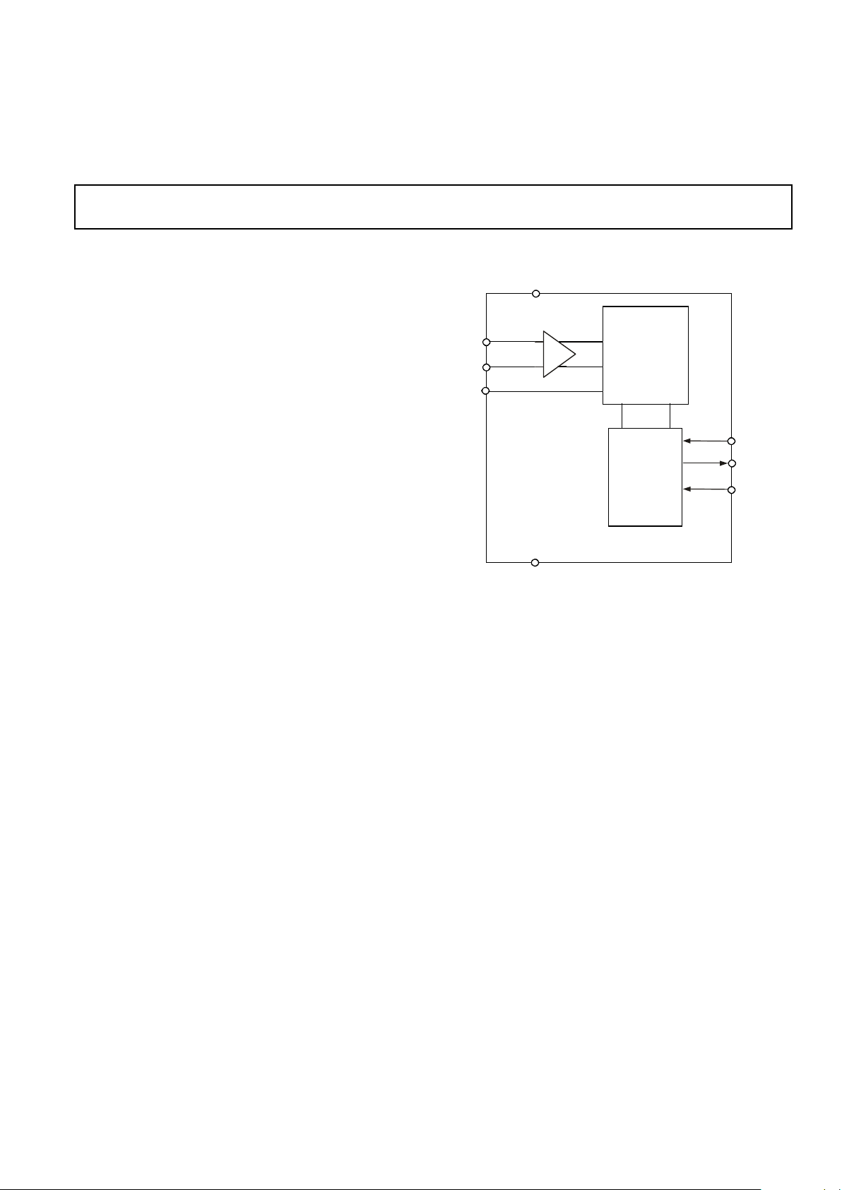
FUNCTIONAL BLOCK DIAGRAM
The SAR architecture of this part ensures that there are
no pipeline delays.
The AD7450 uses advanced design techniques to achieve
very low power dissipation at high throughput rates.
PRODUCT HIGHLIGHTS
1.Operation with either 3 V or 5 V power supplies.
2.High Throughput with Low Power Consumption.
With a 3V supply, the AD7450 offers 3mW typ power
consumption for 833kSPS throughput.
3.Fully Differential Analog Input.
4.Flexible Power/Serial Clock Speed Management.
The conversion rate is determined by the serial clock,
allowing the power to be reduced as the conversion time
is reduced through the serial clock speed increase. This
part also features a shutdown mode to maximize power
efficiency at lower throughput rates.
5.Variable Voltage Reference Input.
6.No Pipeline Delay.
7.Accurate control of the sampling instant via a CS input
and once off conversion control.
8. ENOB > 8 bits typ with 100mV Reference
.
MicroWire is a trademark of National Semiconductor Corporation.
SPI and QSPI are trademarks of Motorola, Inc.
12-BIT SUCCESSIVE
APPROXIMATION
ADC
CONTROL
LO GIC
AD7450
V
IN+
V
IN-
V
REF
GND
SCLK
SDATA
CS
V
DD
T/H
REV. PrJ
PRELIMINARY TECHNICAL DA T A
–2–
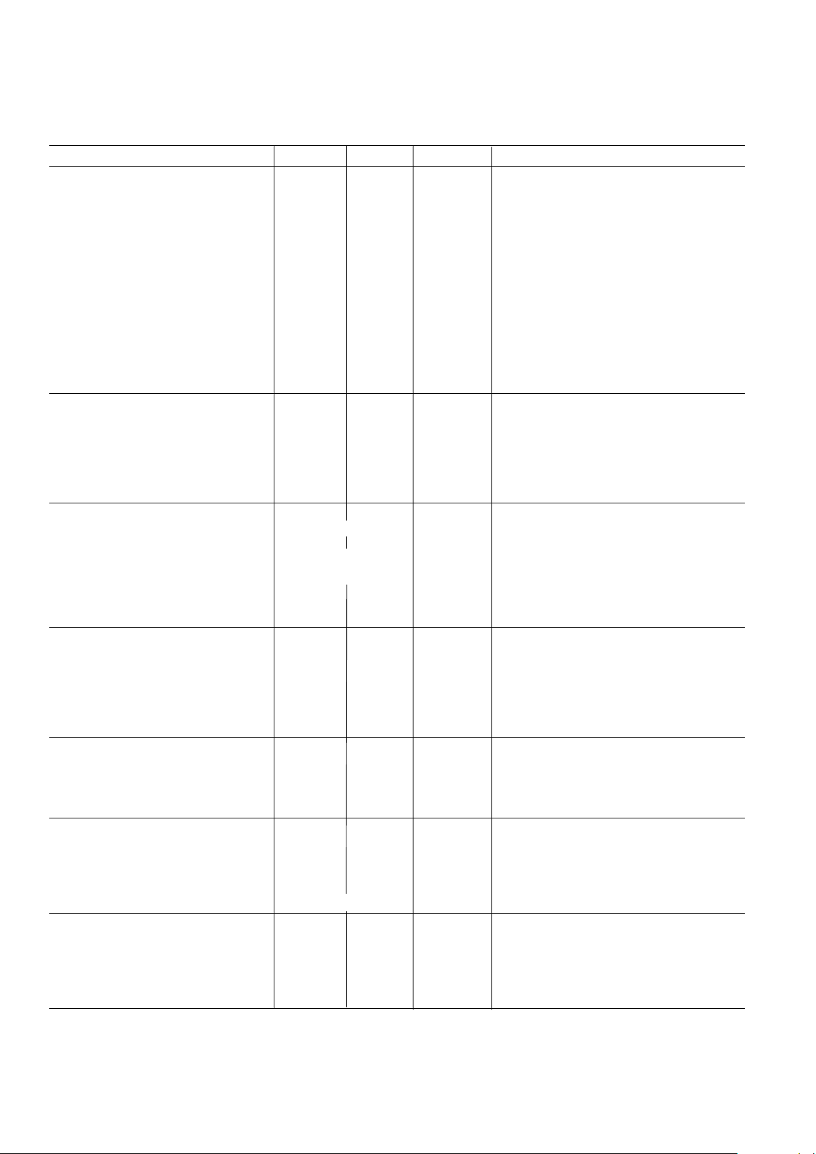
Parameter A Version1B Version1Units Test Conditions/Comments
DYNAMIC PERFORMANCE F
IN
= 300kHz Sine Wave,
f
SAMPLE
= 833kSPS, 1MSPS
Signal to (Noise + Distortion) Ratio 70 70 dB min
(SINAD)
2
Total Harmonic Distortion (THD)2-80 -80 dB max
Peak Harmonic or Spurious Noise
2
-80 -80 dB max
Intermodulation Distortion (IMD)
2
Second Order Terms -78 -78 dB typ
Third Order Terms -78 -78 dB typ
Aperture Delay
3
10 10 ns typ
Aperture Jitter
3
50 50 ps typ
Full Power Bandwidth
3
20 20 MHz typ @ -3 dB
2.5 2.5 MHz typ @ -0.1 dB
Common Mode Rejection Ratio TBD TBD dB
(CMRR)
2
DC ACCURACY
Resolution 12 12 Bits
Integral Nonlinearity (INL)
2
±2 ±1 LSB max
Differential Nonlinearity (DNL)
2
±1 ±1 LSB max Guaranteed No Missed Codes to 12 Bits.
Zero Code Error
2
±5 ±5 LSB max
Positive Gain Error
2
±5 ±5 LSB max
Negative Gain Error
2
±5 ±5 LSB max
ANALOG INPUT
Full Scale Input Span V
IN+
- V
IN -
Volts 2 x V
REF
4
Absolute Input Voltage
V
IN+
V
CM
3
± V
REF
/2 Volts VCM = V
REF
V
IN-
V
CM
3
± V
REF
/2 Volts VCM = V
REF
DC Leakage Current ±1 ±1 µA max
Input Capacitance 20 20 pF typ When in Track
5 5 pF typ When in Hold
REFERENCE INPUT
V
REF
Input Voltage 2.5
5
2.5 Volts 5 V supply (±1% tolerance for specified
performance)
1.25
6
1.25 Volts 3 V supply (±1% tolerance for specified
performance)
DC Leakage Current ±1 ±1 µA max
V
REF
Input Capacitance 15 15 pF typ
LOGIC INPUTS
Input High Voltage, V
INH
2.4 2.4 V min
Input Low Voltage, V
INL
0.8 0.8 V max
Input Current, I
IN
± 1 ± 1 µA max Typically 10 nA, V
IN
= 0 V or V
DD
Input Capacitance, C
IN
7
10 10 pF max
LOGIC OUTPUTS
Output High Voltage, V
OH
2.8 2.8 V min I
SOURCE
= 200µA
Output Low Voltage, V
OL
0.4 0.4 V max I
SINK
=200µA
Floating-State Leakage Current ±10 ±10 µA max
Floating-State Output Capacitance
7
10 10 pF max
Output Coding Two’s Complement
CONVERSION RATE
Conversion Time 16 16 SCLK cycles 888ns with an 18MHz SCLK
1.07µs with a 15MHz SCLK
Track/Hold Acquisition Time
8
275 275 ns max Sine Wave input
Throughput Rate
9
1 1 MSPS max @ VDD = 5V
833 833 kSPS max @ VDD = 3V
AD7450 - SPECIFICATIONS
1
( VDD = 2.7V to 3.3V, f
SCLK
= 15MHz, fS = 833kHz, V
REF
= 1.25 V;
VDD = 4.75V to 5.25V, f
SCLK
= 18MHz, fS = 1MHz, V
REF
= 2.5 V;
V
CM
3
= V
REF
; TA = T
MIN
to T
MAX
, unless otherwise noted.)
REV. PrJ
PRELIMINARY TECHNICAL DA T A
–3–
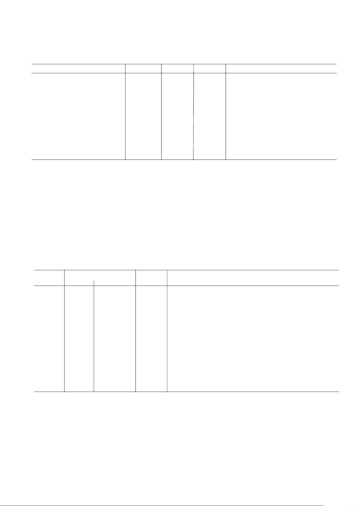
Limit at T
MIN
, T
MAX
Parameter +3V +5V Units Description
f
SCLK
4
10 10 kHz min
15 18 MHz max
t
CONVERT
16 x t
SCLK
16 x t
SCLK
t
SCLK
= 1/f
SCLK
1.07 0.88 µs max SCLK = 15MHz, 18MHz
t
QUIET
50 50 ns min Minimum Quiet Time between the End of a Serial Read and the
Next Falling Edge of CS
t
1
10 10 ns min Minimum CS Pulsewidth
t
2
10 10 ns min CS falling Edge to SCLK Falling Edge Setup Time
t
3
5
20 20 ns max Delay from CS Falling Edge Until SDATA 3-State Disabled
t
4
5
40 40 ns max Data Access Time After SCLK Falling Edge
t
5
0.4 t
SCLK
0.4 t
SCLK
ns min SCLK High Pulse Width
t
6
0.4 t
SCLK
0.4 t
SCLK
ns min SCLK Low Pulse Width
t
7
10 10 ns min SCLK Edge to Data Valid Hold Time
t
8
6
10 10 ns min SCLK Falling Edge to SDATA 3-State Enabled
45 45 ns max SCLK Falling Edge to SDATA 3-State Enabled
t
POWER-UP
7
TBD TBD µs max Power-Up Time from Full Power-Down
NOTES
1
Sample tested at +25°C to ensure compliance. All input signals are specified with tr = tf = 5 ns (10% to 90% of VDD) and timed from a voltage level of 1.6 Volts.
2
See Figure 1 and the “Serial Interface” section.
3
Common Mode Voltage.
4
Mark/Space ratio for the SCLK input is 40/60 to 60/40.
5
Measured with the load circuit of Figure 2 and defined as the time required for the output to cross 0.8 V or 2.4 V with V
DD
= 5 V and time for
an output to cross 0.4 V or 2.0 V for VDD = 3 V.
6
t8 is derived from the measured time taken by the data outputs to change 0.5 V when loaded with the circuit of Figure 2. The measured number is then extrapolated back to remove the effects of charging or discharging the 50 pF capacitor. This means that the time, t
8
, quoted in the
timing characteristics is the true bus relinquish time of the part and is independent of the bus loading.
7
See ‘Power-up Time’ Section.
Specifications subject to change without notice.
Parameter A Version
1
B Version
1
Units Test Conditions/Comments
POWER REQUIREMENTS
V
DD
3/5 3/5 Vmin/max Range: 3 V ± 10%; 5 V ± 5%
I
DD
8,10
Normal Mode(Static) 1 1 mA typ VDD =3 V/5 V. SCLK On or Off
Normal Mode (Operational) 2.6 2.6 mA max V
DD
= 5 V. f
SAMPLE
=1MSPS
2 2 mA max V
DD
= 3 V. f
SAMPLE
=833kSPS
Full Power-Down Mode 1 1 µA max SCLK On or Off
Power Dissipation
Normal Mode (Operational) 13 13 mW max V
DD
=5 V. f
SAMPLE
=1MSPS
6 6 mW max V
DD
=3 V. f
SAMPLE
=833kSPS
Full Power-Down 5 5 µW max V
DD
=5 V. SCLK On or Off
3 3 µW max VDD =3 V. SCLK On or Off
AD7450 - TIMING SPECIFICATIONS
1,2
( VDD = 2.7V to 3.3V, f
SCLK
= 15MHz, fS = 833kHz, V
REF
= 1.25 V;
VDD = 4.75V to 5.25V, f
SCLK
= 18MHz, fS = 1MHz, V
REF
= 2.5 V;
V
CM
3
= V
REF
; TA = T
MIN
to T
MAX
, unless otherwise noted.)
AD7450
NOTES
1
Temperature ranges as follows: A, B Versions: –40°C to +85°C.
2
See ‘Terminology’ section.
3
Common Mode Voltage. The input signal can be centered on any choice of dc Common Mode Voltage as long as this value is in the range
specified in Figure 8.
4
Because the input span of V
IN+
and V
IN-
are both V
REF
, and they are 180° out of phase, the differential voltage is 2 x V
REF
.
5
The reference is functional from 100mV and for 5V supplies it can range up to TBDV (see ‘Reference Section’).
6
The reference is functional from 100mV and for 3V supplies it can range up to 2.2V (see ‘Reference Section’).
7
Sample tested @ +25°C to ensure compliance.
8
See POWER VERSUS THROUGHPUT RATE section.
8
T
CONVERT
+ T
QUIET
(See ‘Serial Interface Section’)
10
Measured with a midscale DC input.
Specifications subject to change without notice.
REV. PrJ
PRELIMINARY TECHNICAL DA T A
–4–
AD7450
CAUTION
ESD (electrostatic discharge) sensitive device. Electrostatic charges as high as 4000 V readily
accumulate on the human body and test equipment and can discharge without detection. Although
the AD7450 features proprietary ESD protection circuitry, permanent damage may occur on devices
subjected to high-energy electrostatic discharges. Therefore, proper ESD precautions are recommended
to avoid performance degradation or loss of functionality.
WARNING!
ESD SENSITIVE DEVICE
ABSOLUTE MAXIMUM RATINGS
1
(TA = +25°C unless otherwise noted)
VDD to GND . . . . . . . . . . . . . . . . . . . . . . . . -0.3 V to +7 V
V
IN+
to GND . . . . . . . . . . . . . . . . . –0.3 V to V
DD
+ 0.3 V
V
IN-
to GND . . . . . . . . . . . . . . . . . –0.3 V to V
DD
+ 0.3 V
Digital Input Voltage to GND . . . -0.3 V to V
DD
+ 0.3 V
Digital Output Voltage to GND . . -0.3 V to V
DD
+ 0.3 V
V
REF
to GND . . . . . . . . . . . . . . . . . . . -0.3 V to V
DD
+0.3 V
Input Current to Any Pin Except Supplies
2
. . . . ±10mA
Operating Temperature Range
Commercial (A, B Version) . . . . . . . . . -40
o
C to +85oC
Storage Temperature Range . . . . . . . . . -65
o
C to +150oC
Junction Temperature . . . . . . . . . . . . . . . . . . . . . . . +150
o
C
SOIC, µSOIC Package, Power Dissipation . . . . 450mW
u
JA
Thermal Impedance . . . . . . . . . . 157°C/W (SOIC)
205.9°C/W (µSOIC)
u
JC
Thermal Impedance . . . . . . . . . . . 56°C/W (SOIC)
43.74°C/W (µSOIC)
Lead Temperature, Soldering
Vapor Phase (60 secs) . . . . . . . . . . . . . . . . . . . +215
o
C
Infared (15 secs) . . . . . . . . . . . . . . . . . . . . . . . +220
o
C
ESD . . . . . . . . . . . . . . . . . . . . . . . . . . . . . . . . . . . . . . . TBD
Linearity Package
Model Range Error (LSB)1Option
4
Branding Information
AD7450AR -40°C to +85°C ±2 LSB SO-8 AD7450AR
AD7450ARM -40°C to +85°C ±2 LSB RM-8 CPA
AD7450BR -40°C to +85°C ±1 LSB SO-8 AD7450BR
AD7450BRM -40°C to +85°C ±1 LSB RM-8 CPB
EVAL-AD7450CB
2
Evaluation Board
EVAL-CONTROL BRD2
3
Controller Board
ORDERING GUIDE
NOTES
1
Linearity error here refers to Integral Linearity Error.
2
This can be used as a stand-alone evaluation board or in conjunction with the EVALUATION BOARD CONTROLLER for evaluation/demonstration purposes.
3
EVALUATION BOARD CONTROLLER. This board is a complete unit allowing a PC to control and communicate with all Analog Devices
evaluation boards ending in the CB designators.
4
S0 = SOIC; RM = µSOIC
NOTES
1
Stresses above those listed under “Absolute Maximum Ratings” may cause permanent
damage to the device. This is a stress rating only and functional operation of the device
at these or any other conditions above those listed in the operational sections of this
specification is not implied. Exposure to absolute maximum rating conditions for
extended periods may affect device reliability.
2
Transient currents of up to 100 mA will not cause SCR latch up.
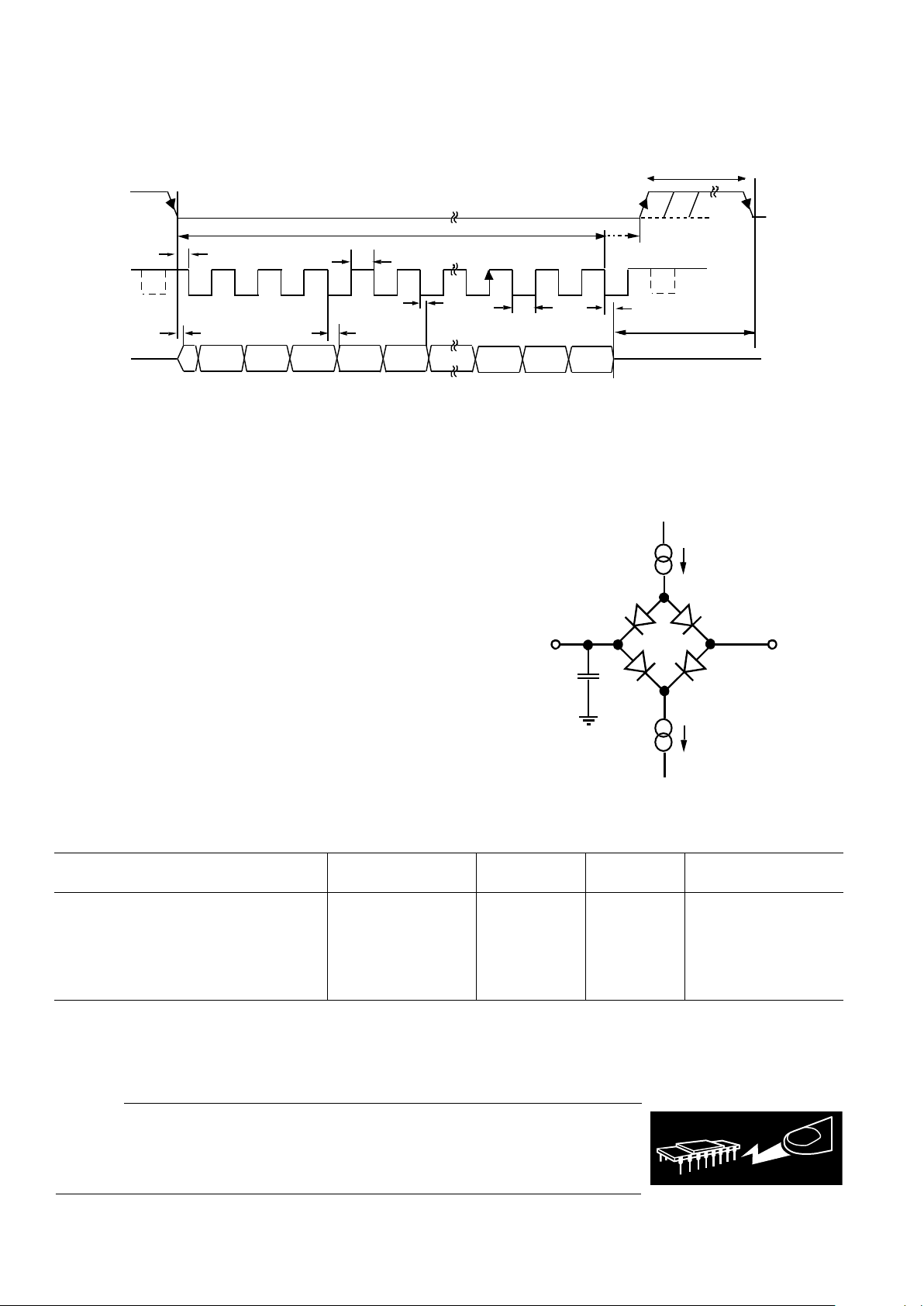
Figure 1. Serial Interface Timing Diagram
Figure 2. Load Circuit for Digital Output Timing Specifications
1 2345 13 161514
t
3
0 0 0 0 DB11 DB10
DB2
DB1 DB0
t
2
4 LEADING ZERO’S
3-STATE
t
4
t
6
t
5
t
7
t
8
t
QUIET
CONV ER T
t
B
C S
SCLK
SDATA
t
1
+1.6V
I
OL
20 0µA
20 0µA
I
OH
TO
OUTPUT
PIN
C
L
50pF
REV. PrJ
PRELIMINARY TECHNICAL DA T A
–5–
AD7450
PIN CONFIGURATION SOIC and µSOIC
PIN FUNCTION DESCRIPTION
Pin No. Pin Mnemonic Function
1V
REF
Reference Input for the AD7450. An external reference must be applied to this input. For a
5 V power supply, the reference is 2.5 V (±1%) and for a 3 V power supply, the reference is
1.25 V (±1%) for specified performance. This pin should be decoupled to GND with a
capacitor of at least 0.1µF. See the ‘Reference Section’ for more details.
2V
IN+
Positive Terminal for Differential Analog Input.
3V
IN-
Negative Terminal for Differential Analog Input.
4 GND Analog Ground. Ground reference point for all circuitry on the AD7450. All analog input
signals and any external reference signal should be referred to this GND voltage.
5 CS Chip Select. Active low logic input. This input provides the dual function of initiating a
conversion on the AD7450 and framing the serial data transfer.
6 SDATA Serial Data. Logic Output. The conversion result from the AD7450 is provided on this
output as a serial data stream. The bits are clocked out on the falling edge of the SCLK
input. The data stream consists of four leading zeros followed by the 12 bits of conversion
data which are provided MSB first. The output coding is two’s complement.
7 SCLK Serial Clock. Logic input. SCLK provides the serial clock for accessing data from the part.
This clock input is also used as the clock source for the AD7450's conversion process.
8V
DD
Power Supply Input. VDD is 3 V (±10%) or 5 V (±5%). This supply should be decoupled to
GND with a 0.1µF Capacitor and a 10µF Tantalum Capacitor.
AD7450
(Not to Scale)
TOP VIEW
1
2
3
4
5
6
7
8
V
REF
V
IN+
V
IN-
GND
CS
SDATA
SCLK
V
DD

REV. PrJ
PRELIMINARY TECHNICAL DA T A
–6–
AD7450
TERMINOLOGY
Signal to (Noise + Distortion) Ratio
This is the measured ratio of signal to (noise + distortion)
at the output of the ADC. The signal is the rms amplitude
of the fundamental. Noise is the sum of all
nonfundamental signals up to half the sampling frequency
(f
S
/2), excluding dc. The ratio is dependent on the number
of quantization levels in the digitization process; the more
levels, the smaller the quantization noise. The theoretical
signal to (noise + distortion) ratio for an ideal N-bit converter with a sine wave input is given by:
Signal to (Noise + Distortion) = (6.02 N + 1.76) dB
Thus for a 12-bit converter, this is 74 dB.
Total Harmonic Distortion
Total harmonic distortion (THD) is the ratio of the rms
sum of harmonics to the fundamental. For the AD7450, it
is defined as:
THD (dB)=20 log
V
2
2
+
V
3
2
+
V
4
2
+
V
5
2
+
V
6
2
V
1
where V1 is the rms amplitude of the fundamental and V2,
V
3
, V4, V5 and V6 are the rms amplitudes of the second to
the sixth harmonics.
Peak Harmonic or Spurious Noise
Peak harmonic or spurious noise is defined as the ratio of
the rms value of the next largest component in the ADC
output spectrum (up to f
S
/2 and excluding dc) to the rms
value of the fundamental. Normally, the value of this
specification is determined by the largest harmonic in the
spectrum, but for ADCs where the harmonics are buried
in the noise floor, it will be a noise peak.
Intermodulation Distortion
With inputs consisting of sine waves at two frequencies, fa
and fb, any active device with nonlinearities will create
distortion products at sum and difference frequencies of
mfa ± nfb where m, n = 0, 1, 2, 3, etc. Intermodulation
distortion terms are those for which neither m nor n are
equal to zero. For example, the second order terms include (fa + fb) and (fa – fb), while the third order terms
include (2fa + fb), (2fa – fb), (fa + 2fb) and (fa – 2fb).
The AD7450 is tested using the CCIF standard where two
input frequencies near the top end of the input bandwidth
are used. In this case, the second order terms are usually
distanced in frequency from the original sine waves while
the third order terms are usually at a frequency close to
the input frequencies. As a result, the second and third
order terms are specified separately. The calculation of the
intermodulation distortion is as per the THD specification
where it is the ratio of the rms sum of the individual distortion products to the rms amplitude of the sum of the
fundamentals expressed in dBs.
Aperture Delay
This is the amount of time from the leading edge of the
sampling clock until the ADC actually takes the sample.
Aperture Jitter
This is the sample to sample variation in the effective
point in time at which the actual sample is taken.
Full Power Bandwidth
The full power bandwidth of an ADC is that input frequency at which the amplitude of the reconstructed
fundamental is reduced by 0.1dB or 3dB for a full scale
input.
Common Mode Rejection Ratio (CMRR)
The Common Mode Rejection Ratio is defined as the
ratio of the power in the ADC output at full-scale frequency, f, to the power of a 200mV p-p sine wave applied
to the Common Mode Voltage of V
IN+
and V
IN-
of fre-
quency fs:
CMRR (dB) = 10log(Pf/Pfs)
Pf is the power at the frequncy f in the ADC output; Pfs is
the power at frequency fs in the ADC output.
Integral Nonlinearity (INL)
This is the maximum deviation from a straight line passing through the endpoints of the ADC transfer function.
Differential Nonlinearity (DNL)
This is the difference between the measured and the ideal 1
LSB change between any two adjacent codes in the ADC.
Zero Code Error
This is the deviation of the midscale code transition (111...111
to 000...000) from the ideal V
IN+-VIN -
(i.e., 0LSB).
Positive Gain Error
This is the deviation of the last code transition (011...110 to
011...111) from the ideal V
IN+-VIN-
(i.e., +V
REF
- 1LSB), after
the Zero Code Error has been adjusted out.
Negative Gain Error
This is the deviation of the first code transition (100...000 to
100...001) from the ideal V
IN+-VIN -
(i.e., -V
REF
+ 1LSB), after
the Zero Code Error has been adjusted out.
Track/Hold Acquisition Time
The track/hold amplifier returns into track mode on the
13th SCLK rising edge (see the “Serial Interface Section”). The track/hold acquisition time is the minimum
time required for the track and hold amplifier to remain in
track mode for its output to reach and settle to within 0.5
LSB of the applied input signal.
Power Supply Rejection (PSR)
The power supply rejection ratio is defined as the ratio of
the power in the ADC output at full-scale frequency, f, to
the power of a 200mV p-p sine wave applied to the ADC
V
DD
supply of frequency fs.
PSRR (dB) = 10 log (Pf/Pfs)
Pf is the power at frequency f in the ADC output; Pfs is
the power at frequency fs in the ADC output.
REV. PrJ
PRELIMINARY TECHNICAL DA T A
–7–
AD7450
PERFORMANCE CURVES
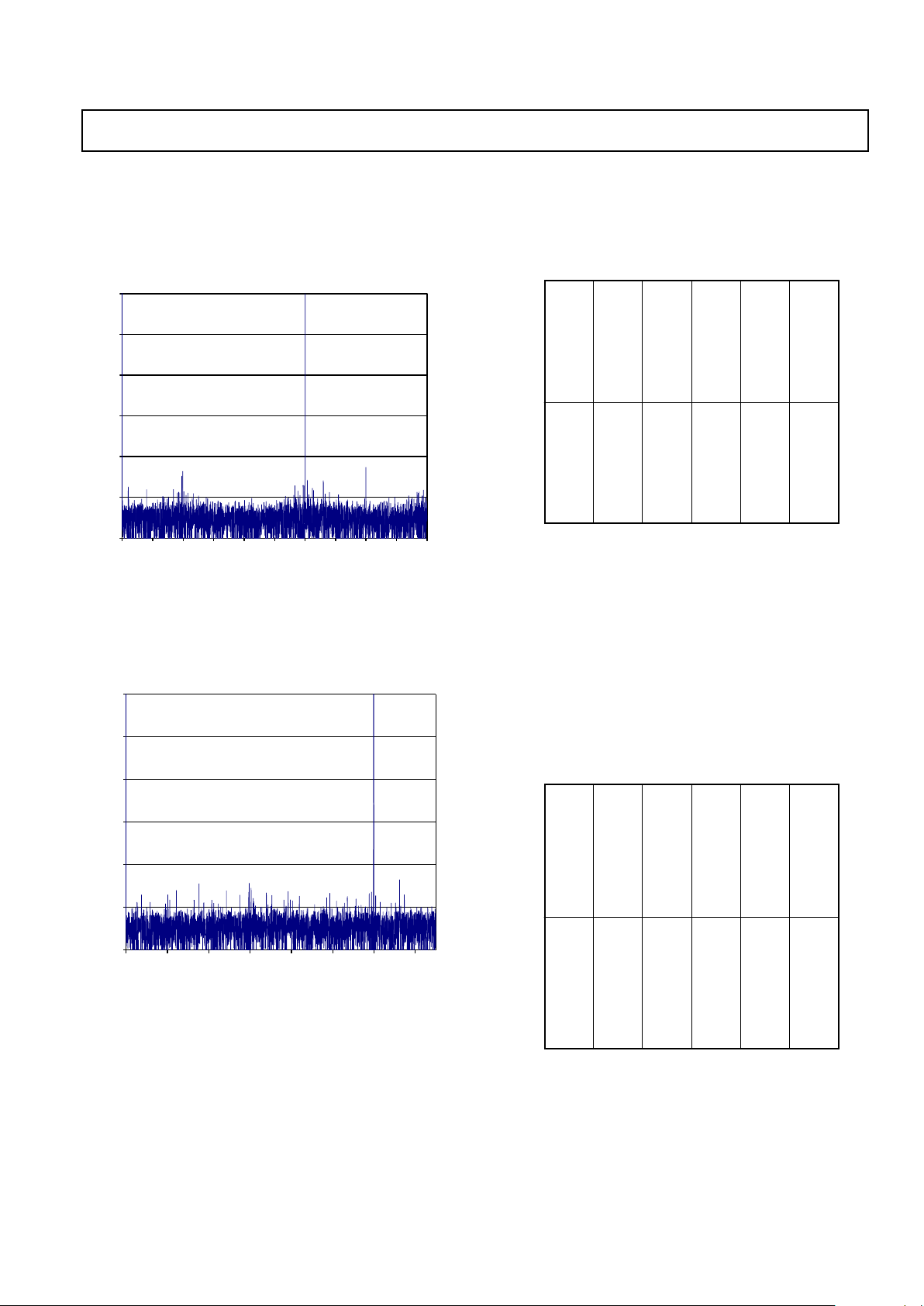
TPC 1 and TPC 2 show the typical FFT plots for the
AD7450 with V
DD
of 5V and 3V, 1MHz and 833kHz sampling frequency respectively and an input frequency of
300kHz.
-120
-100
-80
-60
-40
-20
0
0 50 100 150 200 250 300 350 400 450 500
FREQUENCY (kHz)
SNR (dBs)
8192 POINT FFT
FSAMPLE = 1MSPS
FIN = 300kHz
SINAD = 71.7dB
THD = -82.8dB
SFDR = -85.3dB
TPC 1. AD7450 Dynamic Performance at 1MSPS
with V
DD
=5V
-120
-100
-80
-60
-40
-20
0
0 50 100 150 200 250 300 350
FREQUENCY (kHz)
SNR (dBs)
8192 POINT FFT
f
SAMPLE
= 833ksps
f
IN
= 300kHz
SINAD = 70.2dB
THD = -86dB
SFDR = -87.1dB
TPC 2. AD7450 Dynamic Performance at 833ksps with
V
DD
= 3V
TPC 3 shows the signal-to-(noise+distortion) ratio
performance versus the analog input frequency for
various supply voltages while sampling at 1MSPS
(V
DD
= 5V±5%) and 833kSPS (VDD = 3V±10%).
TITLE
0
0
0
000
T
IT
LE
0000
TPC 3. SINAD vs Analog Input Frequency
for Various Supply Voltages TBD
TPC 4 shows the power supply rejection ratio versus
supply ripple frequency for the AD7450. Here, a
200mV p-p sine wave is coupled onto the V
DD
supply.
A 10nF decoupling capacitor was used on the supply
and a 1µF decoupling capacitor was used on V
REF
.
TITLE
0
0
0
000
T
IT
L
E
0000
TPC 4. Power Supply Rejection (see Terminology Sec-
tion) vs. Supply Ripple Frequency at 5V and 3V TBD
REV. PrJ
PRELIMINARY TECHNICAL DA T A
–8–
AD7450
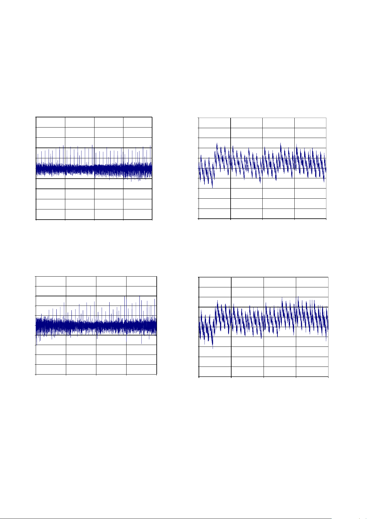
TPC 5 and TPC 6 show typical DNL plots for the
AD7450 with V
DD
of 5V and 3V, 1MHz and 833kHz
sampling frequency respectively and an input frequency of
300kHz.
-1
-0.8
-0.6
-0.4
-0.2
0
0.2
0.4
0.6
0.8
1
0 1024 2048 3072 409 6
CODE
DNL ERROR
(
LSB
)
TPC 5 Typical Differential Nonlinearity (DNL) VDD = 5V
-1
-0.8
-0.6
-0.4
-0.2
0
0.2
0.4
0.6
0.8
1
0 1024 2048 3072 4096
CODE
DNL ERROR
(
LSB
)
TPC 6 Typical Differential Nonlinearity (DNL) VDD = 3V
TPC 7 and TPC 8 show typical INL plots for the
AD7450 with V
DD
of 5V and 3V, 1MHz and 833kHz
sampling frequency respectively and an input frequency of
300kHz.
-1
-0.8
-0.6
-0.4
-0.2
0
0.2
0.4
0.6
0.8
1
0 1024 2048 3072 4096
CODE
INL ERROR
(
LSB
)
TPC 7 Typical Integral Nonlinearity (INL) VDD = 5V
-1
-0.8
-0.6
-0.4
-0.2
0
0.2
0.4
0.6
0.8
1
0 1024 2048 3072 4096
CODE
INL ERROR
(
LSB
)
TPC 8 Typical Integral Nonlinearity (INL) VDD = 3V
 Loading...