Ultralow Noise,
FREQUENCY – Hz
OPEN-LOOP GAIN – dB
PHASE MARGIN – Degrees
120
100
80
60
40
20
0
–20
100 1k 10k 100k 1M
10M 100M
120
100
80
60
40
20
0
–20
PHASE
GAIN
OFFSET
NULL
1
2
3
4
5
6
7
8
AD745
TOP VIEW
NC
OUTPUT
OFFSET
NULL
– IN
+IN
+V
S
–V
S
NC = NO CONNECT
1
2
3
4
5
6
7
89
10
11
12
13
14
16
15
AD745
TOP VIEW
NC
NC
NC
NC NC
NC
NC
NC
NC
OFFSET
NULL
– IN
+IN OUTPUT
OFFSET
NULL
–V
S
+V
S
a
FEATURES
ULTRALOW NOISE PERFORMANCE
2.9 nV/ÏHz at 10 kHz
0.38 mV p-p, 0.1 Hz to 10 Hz
6.9 fA/ÏHz Current Noise at 1 kHz
EXCELLENT AC PERFORMANCE
12.5 V/ms Slew Rate
20 MHz Gain Bandwidth Product
THD = 0.0002% @ 1 kHz
Internally Compensated for Gains of +5 (or –4) or
Greater
EXCELLENT DC PERFORMANCE
0.5 mV max Offset Voltage
250 pA max Input Bias Current
2000 V/mV min Open Loop Gain
Available in Tape and Reel in Accordance with
EIA-481A Standard
APPLICATIONS
Sonar
Photodiode and IR Detector Amplifiers
Accelerometers
Low Noise Preamplifiers
High Performance Audio
PRODUCT DESCRIPTION
The AD745 is an ultralow noise, high speed, FET input
operational amplifier. It offers both the ultralow voltage noise
and high speed generally associated with bipolar input op amps
and the very low input currents of FET input devices. Its 20
MHz bandwidth and 12.5 V/µs slew rate makes the AD745 an
ideal amplifier for high speed applications demanding low noise
and high dc precision. Furthermore, the AD745 does not
exhibit an output phase reversal.
1000
100
R
SOURCE
R
SOURCE
OP37 &
RESISTOR
E
O
( — )
High Speed, BiFET Op Amp
AD745
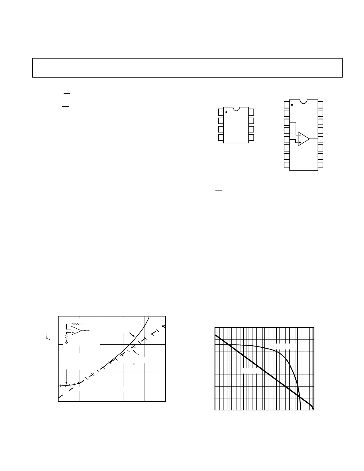
CONNECTION DIAGRAMS
8-Pin Plastic Mini-DIP (N) &
8-Pin Cerdip (Q) Packages
The AD745’s guaranteed, tested maximum input voltage noise
of 4 nV/√
Hz at 10 kHz is unsurpassed for a FET-input monolithic op amp, as is its maximum 1.0 µV p-p noise in a 0.1 Hz to
10 Hz bandwidth. The AD745 also has excellent dc performance with 250 pA maximum input bias current and 0.5 mV
maximum offset voltage.
The internal compensation of the AD745 is optimized for
higher gains, providing a much higher bandwidth and a faster
slew rate. This makes the AD745 especially useful as a
preamplifier where low level signals require an amplifier that
provides both high amplification and wide bandwidth at these
higher gains. The AD745 is available in five performance
grades. The AD745J and AD745K are rated over the
commercial temperature range of 0°C to +70°C. The AD745A
and AD745B are rated over the industrial temperature range of
–40°C to +85°C. The AD745S is rated over the military
temperature range of –55°C to +125°C and is available
processed to MIL-STD-883B, Rev. C.
The AD745 is available in 8-pin plastic mini-DIP, 8-pin cerdip,
16-pin SOIC, or in chip form.
16-Pin SOIC (R) Package
REV. C
Information furnished by Analog Devices is believed to be accurate and
reliable. However, no responsibility is assumed by Analog Devices for its
use, nor for any infringements of patents or other rights of third parties
which may result from its use. No license is granted by implication or
otherwise under any patent or patent rights of Analog Devices.
10
INPUT NOISE VOLTAGE – nV/ Hz
1
100
AD745 & RESISTOR
OR
OP37 & RESISTOR
RESISTOR NOISE ONLY
1k 10k 100k
SOURCE RESISTANCE – Ω
(– – –)
AD745 + RESISTOR
( )
1M 10M
One Technology Way, P.O. Box 9106, Norwood, MA 02062-9106, U.S.A.
Tel: 617/329-4700 Fax: 617/326-8703

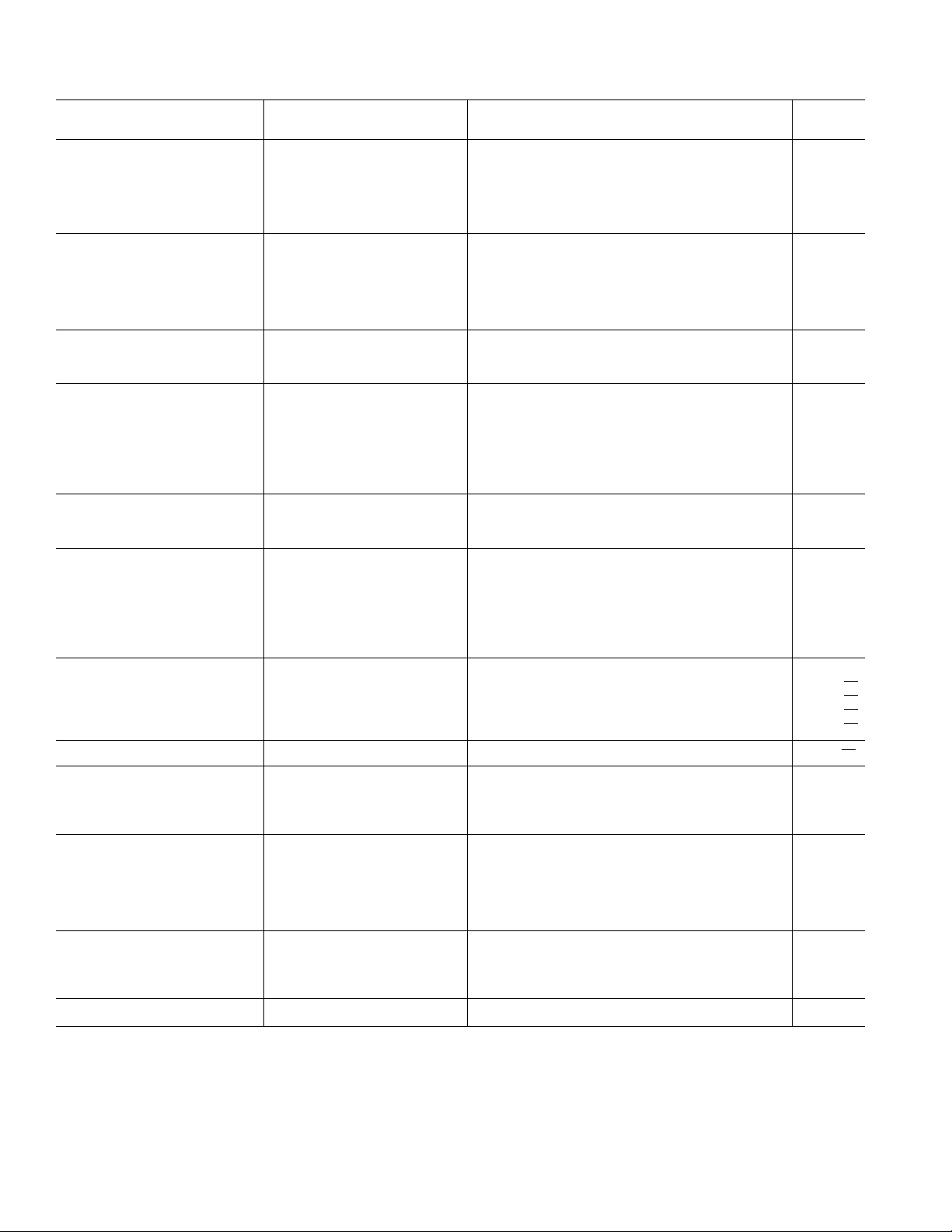
AD745–SPECIFICA TIONS
(@ +258C and 615 V dc, unless otherwise noted)
Model AD745J/A
Conditions Min Typ Max Units
INPUT OFFSET VOLTAGE
1
Initial Offset 0.25 1.0/0.8 mV
Initial Offset T
vs. Temp. T
vs. Supply (PSRR) 12 V to 18 V
vs. Supply (PSRR) T
INPUT BIAS CURRENT
3
MIN
MIN
MIN
to T
to T
to T
MAX
MAX
MAX
2
90 96 dB
2 µV/°C
88 dB
1.5 mV
Either Input VCM = 0 V 150 400 pA
Either Input
@ T
MAX
Either Input VCM = +10 V 250 600 pA
VCM = 0 V 8.8/25.6 nA
Either Input, VS = ±5 V VCM = 0 V 30 200 pA
INPUT OFFSET CURRENT VCM = 0 V 40 150 pA
Offset Current
@ T
MAX
VCM = 0 V 2.2/6.4 nA
FREQUENCY RESPONSE
Gain BW, Small Signal G = –4 20 MHz
Full Power Response VO = 20 V p-p 120 kHz
Slew Rate G = –4 12.5 V/µs
Settling Time to 0.01% 5 µs
Total Harmonic f = 1 kHz
Distortion
4
G = –4 0.0002 %
INPUT IMPEDANCE
Differential 1 × 10¹⁰i20 ΩipF
Common Mode 3 × 10¹¹i18 ΩipF
INPUT VOLTAGE RANGE
Differential
Common-Mode Voltage +13.3, –10.7 V
Over Max Operating Range
5
6
–10 +12 V
±20 V
Common-Mode
Rejection Ratio VCM = ±10 V 80 95 dB
T
MIN
to T
MAX
78 dB
INPUT VOLTAGE NOISE 0.1 to 10 Hz 0.38 µV p-p
f = 10 Hz 5.5 nV/√Hz
f = 100 Hz 3.6 nV/√Hz
f = 1 kHz 3.2 5.0 nV/√Hz
f = 10 kHz 2.9 4.0 nV/√Hz
INPUT CURRENT NOISE f = 1 kHz 6.9 fA/√Hz
OPEN LOOP GAIN VO = ±10 V
R
≥ 2 kΩ 1000 4000 V/mV
LOAD
T
to T
MIN
R
MAX
= 600 Ω 1200 V/mV
LOAD
800 V/mV
OUTPUT CHARACTERISTICS
Voltage R
Current Short Circuit 20 40 mA
≥ 600 Ω +13, –12 V
LOAD
R
≥ 600 Ω +13.6, –12.6 V
LOAD
T
to T
MIN
R
MAX
≥ 2 kΩ±12 +13.8, –13.1 V
LOAD
+12, –10 V
POWER SUPPLY
Rated Performance ±15 V
Operating Range ±4.8 ±18 V
Quiescent Current 8 10.0 mA
TRANSISTOR COUNT # of Transistors 50
NOTES
1
Input offset voltage specifications are guaranteed after 5 minutes of operations at TA = +25°C.
2
Test conditions: +VS = 15 V, –VS = 12 V to 18 V and +VS = 12 V to +18 V, –VS = 15 V.
3
Bias current specifications are guaranteed maximum at either input after 5 minutes of operation at TA = +25°C. For higher temperature, the current doubles every 10°C.
4
Gain = –4, RL = 2 kΩ, CL = 10 pF.
5
Defined as voltagc between inputs, such that neither exceeds ±10 V from common.
6
The AD745 does not exhibit an output phase reversal when the negative common-mode limit is exceeded.
All min and max specifications are guaranteed.
Specifications subject to change without notice.
–2–
REV. C

AD745
ABSOLUTE MAXIMUM RATINGS
Supply Voltage . . . . . . . . . . . . . . . . . . . . . . . . . . . . . . . . ±18 V
Internal Power Dissipation
2
1
Plastic Package . . . . . . . . . . . . . . . . . . . . . . . . . . . . . . 1.3 W
Cerdip Package . . . . . . . . . . . . . . . . . . . . . . . . . . . . . 1.1 W
SOIC Package . . . . . . . . . . . . . . . . . . . . . . . . . . . . . . 1.2 W
Input Voltage . . . . . . . . . . . . . . . . . . . . . . . . . . . . . . . . . . . ±V
S
Output Short-Circuit Duration . . . . . . . . . . . . . . . . Indefinite
Differential Input Voltage . . . . . . . . . . . . . . . . . . +V
and –V
S
S
Storage Temperature Range (Q) . . . . . . . . . –65°C to +150°C
Storage Temperature Range (N, R) . . . . . . . –65°C to +125°C
Operating Temperature Range
AD745J/K . . . . . . . . . . . . . . . . . . . . . . . . . . . 0°C to +70°C
AD745A/B . . . . . . . . . . . . . . . . . . . . . . . . . –40°C to +85°C
AD745S . . . . . . . . . . . . . . . . . . . . . . . . . . –55°C to +125°C
Lead Temperature Range (Soldering 60 sec) . . . . . . . . +300°C
NOTES
1
Stresses above those listed under “Absolute Maximum Ratings” may cause
permanent damage to the device. This is a stress rating only and functional
operation of the device at these or any other conditions above those indicated in the
operational section of this specification is not implied. Exposure to absolute
maximum rating conditions for extended periods may affect device reliability.
2
8-Pin Plastic Package: θJA = 100°C/W, θJC = 50°C/W
8-Pin Cerdip Package: θ
8-Pin Plastic SOIC Package: θJA = 100°C/W, θJC = 30°C/W
= 110°C/W, θJC = 30°C/W
JA
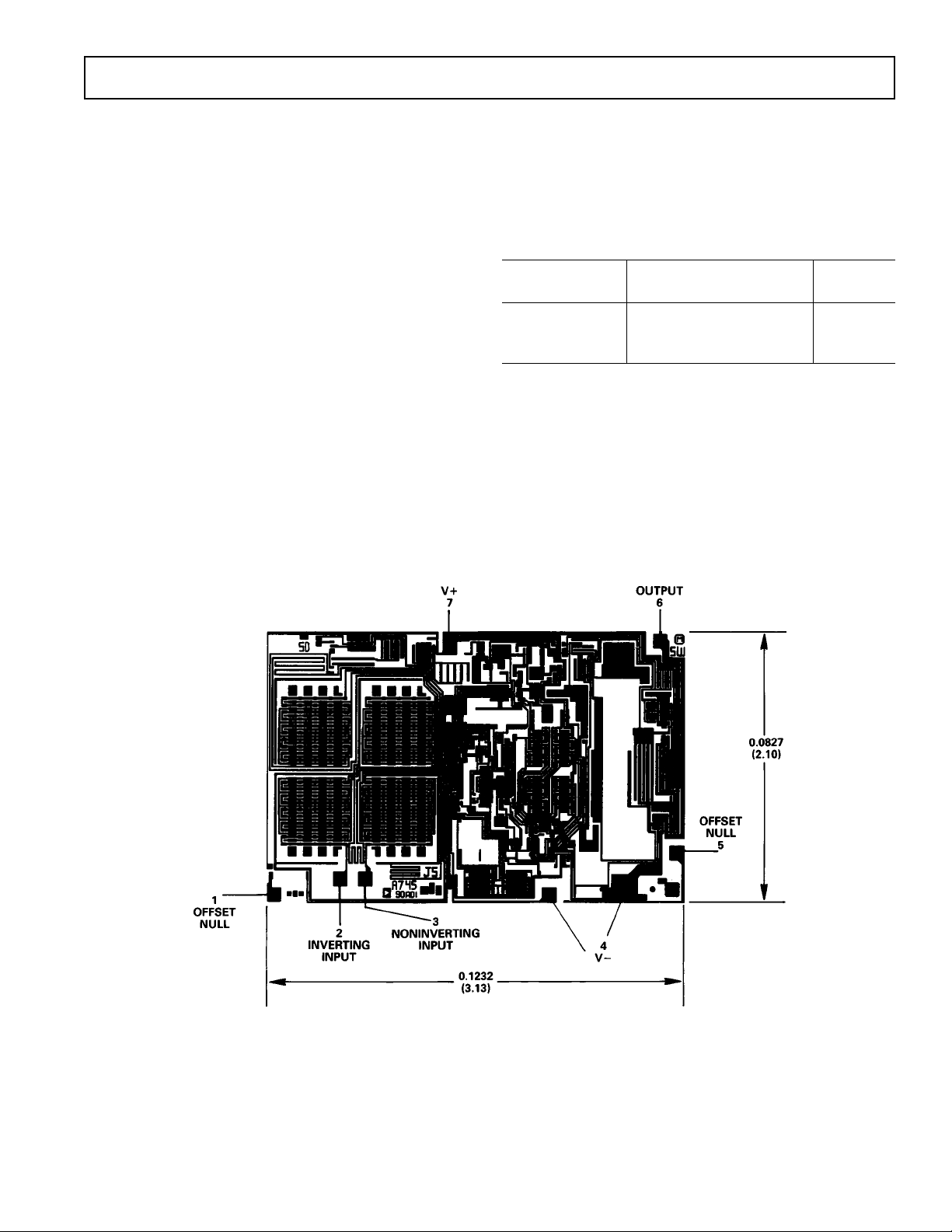
METALIZATION PHOTOGRAPH
Dimensions shown in inches and (mm).
ESD SUSCEPTIBILITY
An ESD classification per method 3015.6 of MIL-STD-883C
has been performed on the AD745, which is a class 1 device.
Using an IMCS 5000 automated ESD tester, the two null pins
will pass at voltages up to 1000 volts, while all other pins will
pass at voltages exceeding 2500 volts.
ORDERING GUIDE
Package
Model Temperature Range Option*
AD745JN 0°C to +70°C N-8
AD745AN –40°C to +85°C N-8
AD745JR-16 0°C to +70°C R-16
*N = Plastic DIP; R = Small Outline IC.
REV. C
–3–

AD745
10
100
1k
10k
LOAD RESISTANCE – Ω
5
10
15
20
25
30
35
0
OUTPUT VOLTAGE SWING – Volts p-p
200
100
10
1
0.1
0.01
10k 100k 1M 10M 100M
FREQUENCY – Hz
OUTPUT IMPEDANCE – Ω
CLOSED-LOOP GAIN = –5
28
26
24
22
20
18
16
14
–60 –40 –20020
40 60 80 100 120 140
GAIN BANDWIDTH PRODUCT – MHz
TEMPERATURE – C
–Typical Characteristics
(@ + 258C, VS = 615 V unless otherwise noted)
20
R = 10kΩ
LOAD
15
10
5
INPUT VOLTAGE SWING – Volts
0
0
5
SUPPLY VOLTAGE VOLTS
+V
IN
–V
IN
10 15 20
+
–
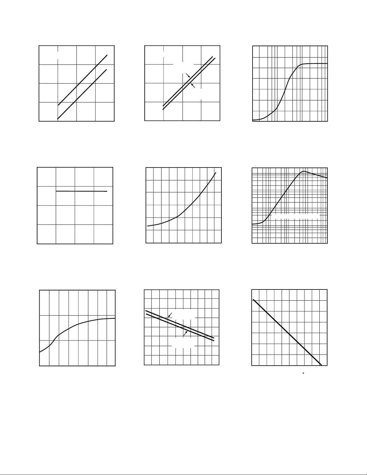
Figure 1. Input Voltage Swing vs.
Supply Voltage
12
9
6
3
QUIESCENT CURRENT – mA
20
R = 10kΩ
LOAD
15
10
5
OUTPUT VOLTAGE SWING – Volts
0
0
POSITIVE
SUPPLY
NEGATIVE
SUPPLY
5101520
SUPPLY VOLTAGE VOLTS
+
–
Figure 2. Output Voltage Swing vs.
Supply Voltage
–6
10
–7
10
–8
10
–9
10
–10
10
–11
INPUT BIAS CURRENT – Amps
10
Figure 3. Output Voltage Swing vs.
Load Resistance
–12
0
0
510
SUPPLY VOLTAGE ± VOLTS
15 20
Figure 4. Quiescent Current vs.
Supply Voltage
300
200
100
INPUT BIAS CURRENT – pA
0
–9 –6 –3 3 6 9
COMMON-MODE VOLTAGE – Volts
Figure 7. Input Bias Current vs.
Common-Mode Voltage
0–12
12
10
–60 –40 –20020 40 60
TEMPERATURE – °C
80 100 120 140
Figure 5. Input Bias Current vs.
Temperature
80
70
60
50
40
30
CURRENT LIMIT – mA
20
10
0
– 60 – 40
+ OUTPUT
CURRENT
– OUTPUT
CURRENT
0 20 40 60 80 100 120 140
– 20
TEMPERATURE – °C
Figure 8. Short Circuit Current Limit
vs. Temperature
Figure 6. Output Impedance vs.
Frequency
Figure 9. Gain Bandwidth Product
vs. Temperature
–4–
REV. C
 Loading...