

Precision, 500 ns Settling
a
FEATURES
AC PERFORMANCE
500 ns Settling to 0.01% for 10 V Step
1.5 s Settling to 0.0025% for 10 V Step
75 V/s Slew Rate
0.0003% Total Harmonic Distortion (THD)
13 MHz Gain Bandwidth – Internal Compensation
>200 MHz Gain Bandwidth (G = 1000)
External Decompensation
>1000 pF Capacitive Load Drive Capability with
10 V/s Slew Rate – External Compensation
DC PERFORMANCE
0.5 mV max Offset Voltage (AD744B)
10 V/ⴗC max Drift (AD744B)
250 V/mV min Open-Loop Gain (AD744B)
Available in Plastic Mini-DIP, Plastic SOIC, Hermetic
Cerdip, Hermetic Metal Can Packages and Chip Form
Surface Mount (SOIC) Package Available in Tape and
Reel in Accordance with EIA-481A Standard
APPLICATIONS
Output Buffers for 12-Bit, 14-Bit and 16-Bit DACs,
ADC Buffers, Cable Drivers, Wideband
Preamplifiers and Active Filters
BiFET Op Amp
AD744
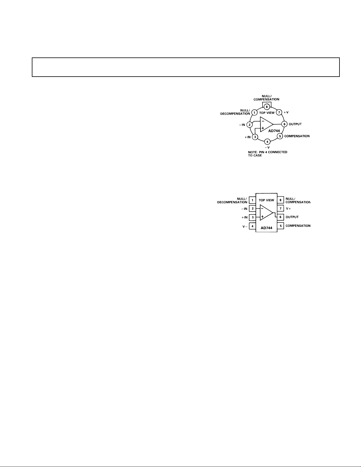
CONNECTION DIAGRAMS
TO-99 (H) Package
8-Lead Plastic Mini-DIP (N)
8-Lead SOIC (R) Package and
8-Lead Cerdip (Q) Packages
PRODUCT DESCRIPTION
The AD744 is a fast-settling, precision, FET input, monolithic
operational amplifier. It offers the excellent dc characteristics
of the AD711 BiFET family with enhanced settling, slew rate,
and bandwidth. The AD744 also offers the option of using
custom compensation to achieve exceptional capacitive load
drive capability.
The single-pole response of the AD744 provides fast settling:
500 ns to 0.01%. This feature, combined with its high dc precision, makes it suitable for use as a buffer amplifier for 12-bit,
14-bit or 16-bit DACs and ADCs. Furthermore, the AD744’s low
total harmonic distortion (THD) level of 0.0003% and gain bandwidth product of 13 MHz make it an ideal amplifier for demanding
audio applications. It is also an excellent choice for use in active
filters in 12-bit, 14-bit and 16-bit data acquisition systems.
The AD744 is internally compensated for stable operation as a
unity gain inverter or as a noninverting amplifier with a gain of
two or greater. External compensation may be applied to the
AD744 for stable operation as a unity gain follower. External
compensation also allows the AD744 to drive 1000 pF capacitive
loads, slewing at 10 V/µs with full stability.
Alternatively, external decompensation may be used to increase
the gain bandwidth of the AD744 to over 200 MHz at high
gains. This makes the AD744 ideal for use as ac preamps in
digital signal processing (DSP) front ends.
The AD744 is available in five performance grades. The AD744J
and AD744K are rated over the commercial temperature range
of 0°C to +70°C. The AD744A and AD744B are rated over
the industrial temperature range of –40°C to +85°C. The AD744T
is rated over the military temperature range of –55°C to +125°C
and is available processed to MIL-STD-883B, Rev. C.
The AD744 is available in an 8-lead plastic mini-DIP, 8-lead
small outline, 8-lead cerdip or TO-99 metal can.
PRODUCT HIGHLIGHTS
1. The AD744 is a high-speed BiFET op amp that offers excellent performance at competitive prices. It outperforms the
OPA602/OPA606, LF356 and LF400.
2. The AD744 offers exceptional dynamic response. It settles to
0.01% in 500 ns and has a 100% tested minimum slew rate
of 50 V/µs (AD744B).
3. The combination of Analog Devices’ advanced processing
technology, laser wafer drift trimming and well-matched
ionimplanted JFETs provide outstanding dc precision. Input
offset voltage, input bias current, and input offset current are
specified in the warmed-up condition; all are 100% tested.
REV. C
Information furnished by Analog Devices is believed to be accurate and
reliable. However, no responsibility is assumed by Analog Devices for its
use, nor for any infringements of patents or other rights of third parties
which may result from its use. No license is granted by implication or
otherwise under any patent or patent rights of Analog Devices.
One Technology Way, P.O. Box 9106, Norwood, MA 02062-9106, U.S.A.
Tel: 781/329-4700 World Wide Web Site: http://www.analog.com
Fax: 781/326-8703 © Analog Devices, Inc., 2000
AD744–SPECIFICATIONS
(@ +25ⴗC and ⴞ15 V dc, unless otherwise noted)
Model Conditions Min Typ Max Min Typ Max Unit
AD744J/A/S AD744K/B/T
INPUT OFFSET VOLTAGE
1
Initial Offset 0.3 1.0 0.25 0.5 mV
Offset T
vs. Temp. 5 20 5 10 µV/°C
vs. Supply
2
vs. Supply T
Long-Term Stability 15 15 µV/month
INPUT BIAS CURRENT
3
MIN
MIN
to T
to T
MAX
MAX
2 1.0 mV
82 95 88 100 dB
82 88 dB
Either Input VCM = 0 V 30 100 30 100 pA
Either Input @ T
J, K 70°C 0.7 2.3 0.7 2.3 nA
=V
MAX
CM
= 0 V
A, B, C 85°C 1.9 6.4 1.9 6.4 nA
S, T 125°C 31 102 31 102 nA
Either Input VCM = +10 V 40 150 40 150 pA
Offset Current VCM = 0 V 20 50 10 50 pA
Offset Current @ T
J, K 70°C 0.4 1.1 0.2 1.1 nA
=V
MAX
CM
= 0 V
A, B, C 85°C 1.3 3.2 0.6 3.2 nA
S, T 125°C20521052nA
FREQUENCY RESPONSE
Gain BW, Small Signal G = –1 8 13 9 13 MHz
Full Power Response V
Slew Rate, Unity Gain G = –1 45 75 50 75 V/µs
Settling Time to 0.01%
4
= 20 V p-p 1.2 1.2 MHz
O
G = –1 0.5 0.75 0.5 0.75 µs
Total Harmonic f = 1 kHz
Distortion R1 ≥ 2 kΩ
VO = 3 V rms 0.0003 0.0003 %
INPUT IMPEDANCE
Differential 3 ⫻ 1012||5.5 3 ⫻ 1012||5.5 Ω||pF
Common Mode 3 ⫻ 1012||5.5 3 ⫻ 1012||5.5 Ω||pF
INPUT VOLTAGE RANGE
Differential
Common-Mode Voltage +14.5, –11.5 +14.5, –11.5 V
Over Max Operating Range
5
6
–11 +13 –11 +13 V
±20 ±20 V
Common-Mode
Rejection Ratio VCM = ±10 V 78 88 82 88 dB
T
to T
MIN
MIN
to T
MAX
MAX
VCM = ±11 V 72 84 78 84 dB
T
76 84 80 84 dB
70 80 74 80 dB
INPUT VOLTAGE NOISE 0.1 to 10 Hz 2 2 µV p-p
f = 10 Hz 45 45 nV/√Hz
f = 100 Hz 22 22 nV/√Hz
f = 1 kHz 18 18 nV/√Hz
f = 10 kHz 16 16 nV/√Hz
INPUT CURRENT NOISE f = 1 kHz 0.01 0.01 pA/√Hz
OPEN LOOP GAIN
7
VO = ±10 V
R
≥ 2 kΩ 200 400 250 400 V/mV
LOAD
T
MIN
to T
MAX
100 100 V/mV
OUTPUT CHARACTERISTICS
Voltage R
Current Short Circuit 25 25 mA
Capacitive Load
8
≥ 2 kΩ +13, –12.5 +13.9, –13.3 +13, –12.5 +13.9, –13.3 V
LOAD
T
MIN
to T
MAX
±12 +13.8, –13.1 ± 12 +13.8, –13.1 V
Gain = –1 1000 1000 pF
POWER SUPPLY
Rated Performance ±15 ±15 V
Operating Range ± 4.5 ± 18 ±4.5 ±18 V
Quiescent Current 3.5 5.0 3.5 4.0 mA
NOTES
1
Input offset voltage specifications are guaranteed after 5 minutes of operation at TA = +25°C.
2
PSRR test conditions: +VS = 15 V, –VS = –12 V to –18 V and +VS = +12 V to +18 V, –VS = –15 V.
3
Bias Current Specifications are guaranteed maximum at either input after 5 minutes of operation at TA = +25°C. For higher temperature, the current doubles every 10°C.
4
Gain = –1, RL = 2 k, CL = 10 pF, refer to Figure 25.
5
Defined as voltage between inputs, such that neither exceeds ±10 V from ground.
6
Typically exceeding –14.1 V negative common-mode voltage on either input results in an output phase reversal.
7
Open-Loop Gain is specified with VOS both nulled and unnulled.
8
Capacitive load drive specified for C
Refer to Table II for optimum compensation while driving a capacitive load.
Specifications subject to change without notice. All min and max specifications are guaranteed.
= 20 pF with the device connected as shown in Figure 32. Under these conditions, slew rate = 14 V/µs and 0.01% settling time = 1.5 µs typical.
COMP
–2–
REV.C
AD744
ABSOLUTE MAXIMUM RATINGS
Supply Voltage . . . . . . . . . . . . . . . . . . . . . . . . . . . . . . . . ±18 V
Internal Power Dissipation
Input Voltage
3
. . . . . . . . . . . . . . . . . . . . . . . . . . . . . . . . ±18 V
2
. . . . . . . . . . . . . . . . . . . . 500 mW
1
Output Short Circuit Duration . . . . . . . . . . . . . . . . Indefinite
Differential Input Voltage . . . . . . . . . . . . . . . . . . +V
and –V
S
S
Storage Temperature Range (Q, H) . . . . . . –65°C to +150°C
Storage Temperature Range (N, R) . . . . . . . –65°C to +125°C
Operating Temperature Range
AD744J/K . . . . . . . . . . . . . . . . . . . . . . . . . . . 0°C to +70°C
AD744A/B . . . . . . . . . . . . . . . . . . . . . . . . . –40°C to +85°C
AD744S/T . . . . . . . . . . . . . . . . . . . . . . . . –55°C to +125°C
Lead Temperature Range (Soldering 60 seconds) . . . . . 300°C
NOTES
1
Stresses above those listed under Absolute Maximum Ratings may cause perma-
nent damage to the device. This is a stress rating only; functional operation of the
device at these or any other conditions above those indicated in the operational
section of this specification is not implied. Exposure to absolute maximum rating
conditions for extended periods may affect device reliability.
2
Thermal Characteristics
8-Lead Plastic Package: θJA = 100°C/Watt, θJC = 33°C/Watt
8-Lead Cerdip Package: θJA = 110°C/Watt, θJC = 22°C/Watt
8-Lead Metal Can Package: θJA = 150°C/Watt, θJC = 65°C/Watt
8-Lead SOIC Package: θJA = 160°C/Watt, θJC = 42°C/Watt
3
For supply voltages less than ± 18 V, the absolute maximum input voltage is equal
to the supply voltage.
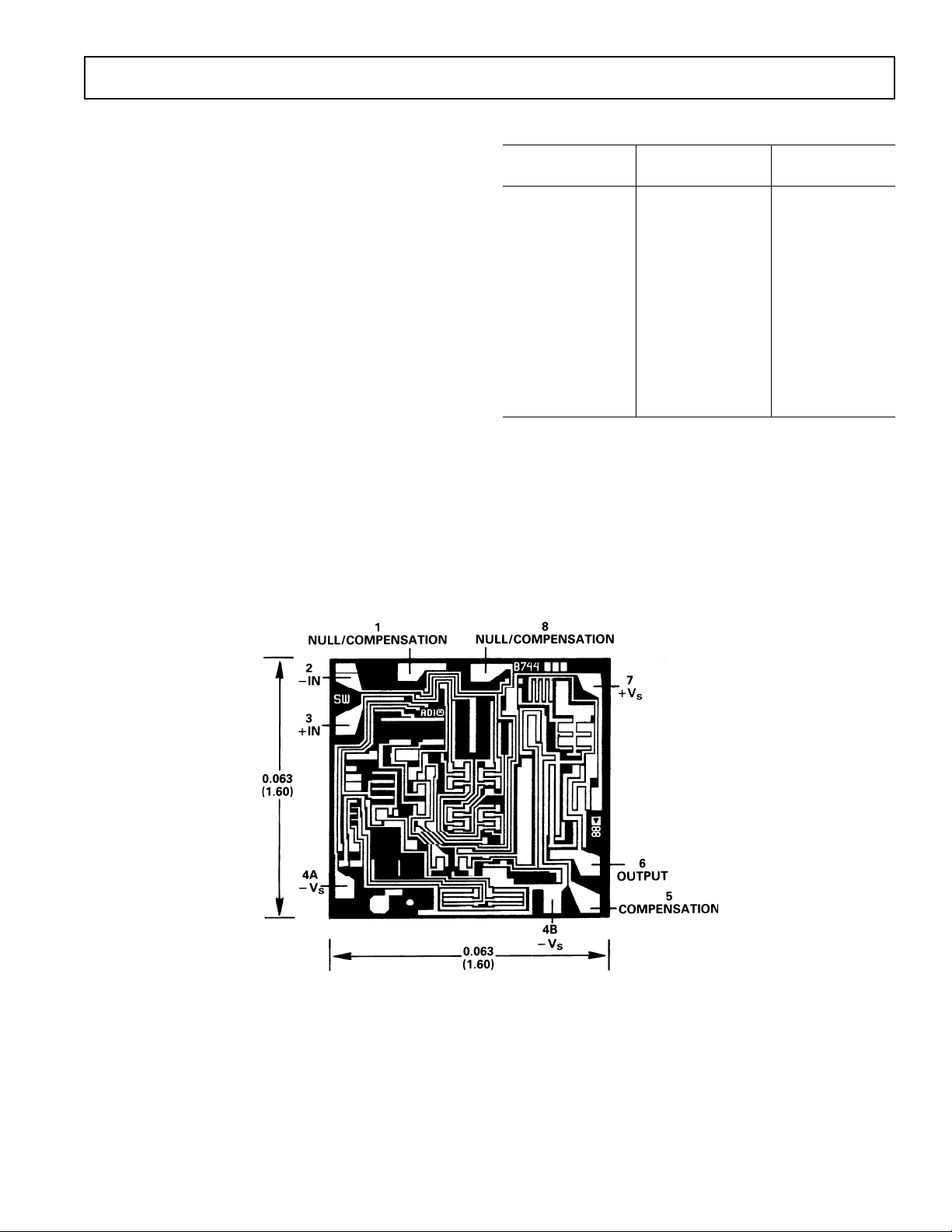
METALIZATION PHOTOGRAPH
Contact factory for latest dimensions.
Dimensions shown in inches and (mm).
ORDERING GUIDE
Temperature Package
Model Range Option*
AD744JN 0°C to +70°C N-8
AD744KN 0°C to +70°C N-8
AD744JR 0°C to +70°C SO-8
AD744KR 0°C to +70°C SO-8
AD744AQ –40°C to +85°C Q-8
AD744BQ –40°C to +85°C Q-8
AD744AH –40°C to +85°C H-08A
AD744JCHIPS 0°C to +70°CDie
AD744JR-REEL 0°C to +70°C Tape/Reel 13"
AD744JR-REEL 7 0°C to +70°C Tape/Reel 7"
AD744KR-REEL 0°C to +70°C Tape/Reel 13"
AD744KR-REEL 7 0°C to +70°C Tape/Reel 7"
AD744TA/883B –55°C to +125°C H-08
*N = Plastic DIP; SO = Small Outline IC; Q = Cerdip; H = TO-99 Metal Can.
REV. C
–3–
AD744
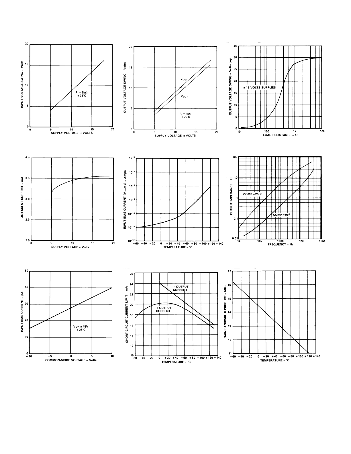
–Typical Characteristics
Figure 1. Input Voltage Swing
vs. Supply Voltage
Figure 4. Quiescent Current vs.
Supply Voltage
Figure 2. Output Voltage Swing
vs. Supply Voltage
Figure 5. Input Bias Current vs.
Temperature
Figure 3. Output Voltage Swing vs.
Load Resistance
Figure 6. Output Impedance vs.
Frequency
Figure 7. Input Bias Current vs.
Common-Mode Voltage
Figure 8. Short Circuit Current
Limit vs. Temperature
–4–
Figure 9. Gain Bandwidth
Product vs. Temperature
REV. C

AD744
Figure 10. Open-Loop Gain and
Phase Margin vs. Frequency
= 0 pF
C
COMP
Figure 13. Common-Mode and
Power Supply Rejection vs.
Frequency
Figure 11. Open Loop Gain and
Phase Margin vs. Frequency
C
= 25 pF
COMP
Figure 14. Large Signal Frequency
Response
Figure 12. Open-Loop Gain vs.
Supply Voltage
Figure 15. Output Swing and Error
vs. Settling Time
Figure 16. Total Harmonic Distortion
vs. Frequency, Circuit of Figure 20
(G = 10)
REV. C
Figure 17. Input Noise Voltage
Spectral Density
–5–
Figure 18. Slew Rate vs. Input
Error Signal

AD744
–Typical Characteristics
Figure 19. Settling Time vs. Closed
Loop Voltage Gain
Figure 22a. Unity-Gain Follower
Figure 20. THD Test Circuit
Figure 22b. Unity-Gain Follower
Large Signal Pulse Response,
C
= 5 pF
COMP
Figure 21. Offset Null Configuration
Figure 22c. Unity-Gain Follower
Small Signal Pulse Response,
C
= 5 pF
COMP
Figure 23a. Unity-Gain Inverter
Figure 23b. Unity-Gain Inverter Large
Signal Pulse Response, C
COMP
= 5 pF
–6–
Figure 23c. Unity-Gain Inverter Small
Signal Pulse Response, C
COMP
= 0 pF
REV. C

AD744
POWER SUPPLY BYPASSING
The power supply connections to the AD744 must maintain a
low impedance to ground over a bandwidth of 10 MHz or more.
This is especially important when driving a significant resistive
or capacitive load, since all current delivered to the load comes
from the power supplies. Multiple high quality bypass capacitors
are recommended for each power supply line in any critical
application. A 0.1 µF ceramic and a 1 µF electrolytic capacitor
as shown in Figure 24 placed as close as possible to the amplifier (with short lead lengths to power supply common) will
assure adequate high frequency bypassing, in most applications. A minimum bypass capacitance of 0.1 µF should be used
for any application.
+V
S
1F
0.1F
AD744
1F
–V
S
0.1F
Figure 24. Recommended Power Supply Bypassing
MEASURING AD744 SETTLING TIME
The photos of Figures 26 and 27 show the dynamic response of
the AD744 while operating in the settling time test circuit of
Figure 25. The input of the settling time fixture is driven by a
flat-top pulse generator. The error signal output from the false
summing node of A1, the AD744 under test, is clamped, amplified by op amp A2 and then clamped again.
The error signal is thus clamped twice: once to prevent overloading
amplifier A2 and then a second time to avoid overloading the
oscilloscope preamp. A Tektronix oscilloscope preamp type
7A26 was carefully chosen because it recovers from the
approximately 0.4 V overload quickly enough to allow accurate
measurement of the AD744’s 500 ns settling time. Amplifier A2
is a very high-speed FET-input op amp; it provides a voltage
gain of 10, amplifying the error signal output of the AD744
under test.
Figure 26. Settling Characteristics 0 to +10 V Step
Upper Trace: Output of AD744 Under Test (5 V/div.)
Lower Trace: Amplified Error Voltage (0.01%/div.)
+15V
COM
–15V
2X
HP2835
FLAT-TOP
PULSE
GENERATOR
DATA
DYNAMICS
5109
OR
EQUIVALENT
TO
+V
S
–V
S
A2
AD3554
0.47F
1.1k⍀
–V
S
4.99k⍀
V
10k⍀
IN
1F
0.1F
NOTE: USE CIRCUIT BOARD WITH GROUND PLANE
TEKTRONIX
7A26
OSCILLOSCOPE
PREAMP
INPUT SECTION
5pF
(VIA LESS THAN 1 FT 50⍀
COAXIAL CABLE)
0.47F
+V
S
10k⍀
0.2pF – 0.8pF
NULL
200⍀
5pF – 18pF
AD744
A1
+V
–V
S
206⍀
4.99k⍀
10k⍀
S
5k⍀
1F
1M⍀ 20pF
V
ERROR
2X
HP2835
0.1F
Figure 25. Settling Time Test Circuit
ⴛ 10
Figure 27. Settling Characteristics 0 to –10 V Step
Upper Trace: Output of AD744 Under Test (5 V/div.)
Lower Trace: Amplified Error Voltage (0.01%/div.)
10pF
REV. C
–7–

AD744
EXTERNAL FREQUENCY COMPENSATION
Even though the AD744 is useable without compensation in
most applications, it may be externally compensated for even
more flexibility. This is accomplished by connecting a capacitor
between Pins 5 and 8. Figure 28, a simplified schematic of the
AD744, shows where this capacitor is connected. This feature is
useful because it allows the AD744 to be used as a unity gain
voltage follower. It also enables the amplifier to drive capacitive
loads up to 2000 pF and greater.
+V
S
OUTPUT
COMPENSATION
–V
S
–IN
COMPENSATION
DECOMPENSATION
NULL /
NULL /
300⍀
300⍀
1k⍀1k⍀ 8k⍀
+IN
2mA400A
5pF
Figure 28. AD744 Simplified Schematic
The slew rate and gain bandwidth product of the AD744 are inversely proportional to the value of the compensation capacitor,
. Therefore, when trying to maximize the speed of the
C
COMP
amplifier, the value of C
should be minimized. C
COMP
COMP
can
also be used to slow the amplifier to a point where the slew rate
is perfectly symmetrical and well controlled. Figure 29 summarizes the effect of external compensation on slew rate and
bandwidth.
0.2
GAIN BANDWIDTH – MHz
20
2
100
10
1.0
SLEW RATE – V/s
The following section provides tables to show what C
COMP
values
will provide the necessary compensation for given circuit configurations
and capacitive loads. In each case, the recommended C
minimum value. A larger C
can always be used, but slew rate
COMP
COMP
is a
and bandwidth performance will be degraded.
Figure 30 shows the AD744 configured as a unity gain voltage
follower. In this case, a minimum compensation capacitor of
5 pF is necessary for stable operation. Larger compensation capacitors can be used for driving larger capacitive loads. Table I
outlines recommended minimum values for C
COMP
based on
the desired capacitive load. It also gives the slew rate and bandwidth that will be achieved for each case.
+V
S
1F 0.1F
AD744
V
IN
–V
S
C
COMP
1F 0.1F
5pF
V
OUT
Figure 30. AD744 Connected as a Unity Gain
Voltage Follower
Table I. Recommended Values of C
COMP
vs.
Various Capacitive Loads
Max –3 dB
C
LOAD
C
COMP
Slew Rate Bandwidth
Gain (pF) (pF) (V/s) (MHz)
1 50 5 37 6.5
1 150 10 25 4.3
1 2000 25 12.5 2.0
Figures 31 and 32 show the AD744 as a voltage follower
with gain and as an inverting amplifier. In these cases, external
compensation is not necessary for stable operation. However, compensation may be applied to drive capacitive loads
above 50 pF. Table II gives recommended C
values, along
COMP
with expected slew rates and bandwidths for a variety of load
conditions and gains for the circuits in Figures 31 and 32.
0.02
0
10 100 1000
C
– pF
COMP
Figure 29. Gain Bandwidth and Slew Rate vs. C
0.1
COMP
C
*
LEAD
R1*
R2*
+V
S
1F
0.1F
AD744
1F
C
COMP
OPTIONAL
0.1F
V
IN
*SEE TABLE II
–V
S
Figure 31. AD744 Connected as a Voltage Follower
Operating at Gains of 2 or Greater
–8–
V
OUT
REV. C

AD744
Table II. Recommended Values of C
vs. Various Load Conditions for the Circuits of
COMP
Figures 31 and 32.
Max Slew –3 dB
R1 R2 Gain Gain C
LOAD
(⍀)(⍀) Follower Inverter (pF) (pF) (pF) (V/s) (MHz)
4.99 k 4.99 k 2 1 50 0 7 75 2.5
4.99 k 4.99 k 2 1 150 5 7 37 2.3
4.99 k 4.99 k 2 1 1000 20 – 14 1.2
4.99 k 4.99 k 2 1 >2000 25 – 12.5
499 Ω 4.99 k 11 10 270 0 – 75 1.2
499 Ω 4.99 k 11 10 390 2 – 50 0.85
499 Ω 4.99 k 11 10 1000 5 – 37
NOTES
1
Bandwidth with C
2
Into large capacitive loads the AD744’s 25 mA output current limit sets the slew rate of the amplifier, in V/ µs, equal to 0.025
amps divided by the value of C
specified with a 50 pF. load.
C
LEAD
R1*
V
IN
AD744
*SEE TABLE II
–V
S
adjusted for minimum settling time.
LEAD
in µF. Slew rate is specified into rated max C
LOAD
*
R2*
+V
S
1F
C
1F
COMP
0.1F
OPTIONAL
0.1F
V
OUT
Figure 32. AD744 Connected as an Inverting Amplifier
Operating at Gains of 1 or Greater
Using Decompensation to Extend the Gain Bandwidth
Product
When the AD744 is used in applications where the closed-loop
gain is greater than 10, gain bandwidth product may be enhanced
by connecting a small capacitor between Pins 1 and 5 (Figure
33). At low frequencies, this capacitor cancels the effects of the
chip’s internal compensation capacitor, C
, effectively dec-
COMP
ompensating the amplifier.
C
COMPCLEAD
except for cases marked 2, which are
LOAD
Rate Bandwidth
1
1
2
2
1.0
0.60
Due to manufacturing variations in the value of the internal
, it is recommended that the amplifier’s response be
C
COMP
optimized for the desired gain by using a 2 to 10 pF trimmer
capacitor rather than using a fixed value.
R1*
AD744
V
IN
\
–V
S
R2*
+V
S
1F
2 – 10pF
1F
0.1F
NOT CONNECTED
*SEE TABLE III
0.1F
V
OUT
Figure 33. Using the Decompensation Connection to
Extend Gain Bandwidth
Table III. Performance Summary for the Circuit of Figure 33
R1 R2 Gain Gain –3 dB Gain/BW
(⍀)(⍀) Follower Inverter Bandwidth Product
1 k 10 k 11 10 2.5 MHz 25 MHz
100 10 k 101 100 760 kHz 76 MHz
100 100 k 1001 1000 225 kHz 225 MHz
REV. C
–9–

AD744
GAIN
ADJUST
100⍀
REF
REF
GND
BIPOLAR
OFFSET
0.1F
V
10V
20k⍀
CC
AD565A
REF
OUT
19.95k⍀
IN
100⍀
9.96k⍀
ADJUST
5k⍀
5k⍀
8k⍀
20V SPAN
10V SPAN
DAC OUT
C
10pF
LEAD
+15V
AD744
1F
1F
0.1F
POWER
GND
–V
EE
MSB
LSB
Figure 34.±10 V Voltage Output Bipolar DAC Using the AD744 as an Output Buffer
HIGH-SPEED OP AMP APPLICATIONS AND TECHNIQUES
DAC Buffers (I-to-V Converters)
Digital-to-analog converters which use bipolar transistors to
switch currents into (or out of) their outputs can achieve very
fast settling times. The AD565A, for example, is specified to
settle to 12 bits in less than 250 ns, with a current output. However, in many applications, a voltage output is desirable, and it
would be useful – perhaps essential – that this I-to-V conversion
be accomplished without increasing the settling time or without
degrading the accuracy of the DAC.
Figure 34 is a schematic of an AD565A DAC using an AD744
output buffer. The 10 pF C
capacitor compensates for the
LEAD
DAC’s output capacitance, plus the 5.5 pF amplifier input
capacitance.
Figure 35 is an oscilloscope photo of the AD744’s output voltage with a +10 V to 0 V step applied; this corresponds to an all
“1s” to all “0s” code change on the DAC. Since the DAC is
–15V
A HIGH-SPEED, 3 OP AMP INSTRUMENTATION AMPLIFIER CIRCUIT
The instrumentation amplifier circuit shown in Figure 36 can
provide a range of gains from unity up to 1000 and higher. The
circuit bandwidth is 4 MHz at a gain of 1 and 750 kHz at a gain
of 10; settling time for the entire circuit is less than 2 µs
to within 0.01% for a 10 V step, (G = 10).
While the AD744 is not stable with 100% negative feedback (as
when connected as a standard voltage follower), phase margin
and therefore stability at unity gain may be increased to an acceptable level by placing the parallel combination of a resistor and a
small lead capacitor between each amplifier’s output and its
inverting input terminal.
The only penalty associated with this method is a small bandwidth reduction at low gains. The optimum value for C
LEAD
may be determined from the graph of Figure 41. This technique
can be used in the circuit of Figure 36 to achieve stable operation at gains from unity to over 1000.
20,000
R
G
*1.5pF – 20pF
(TRIM FOR BEST SETTLING TIME)
**10k⍀
**10k⍀
**10k⍀
5pF
A3
AD744
**10k⍀
SENSE
–IN
CIRCUIT GAIN = + 1
AD744
A1
7.5pF
7.5pF
R
G
10k⍀
10k⍀
Figure 35. Upper Trace: AD744 Output Voltage for
a +10 V to 0 V Step, Scale: 5 mV/div.
Lower Trace: Logic Input Signal, Scale: 5 V/div.
connected in the 20 V span mode, 1 LSB is equal to 4.88 mV.
Output settling time for the AD565/AD744 combination is less
than 500 ns to within a 2.44 mV, 1/2 LSB error band.
–10–
+IN
A2
AD744
*VOLTRONICS SP20 TRIMMER CAPACITOR OR EQUIVALENT
**RATIO MATCHED 1% METAL FILM RESISTORS
+15V
COMM
–15V
FOR OPTIONAL OFFSET ADJUSTMENT:
TRIM A1, A3 USING TRIM PROCEDURE SHOWN IN FIGURE 21.
1F
1F
+V
S
–V
S
1F
1F
0.1F
0.1F
Figure 36. A High Performance, 3 Op Amp
Instrumentation Amplifier Circuit
REFERENCE
PIN 7
EACH
AMPLIFIER
PIN 4
REV. C

AD744
Table IV. Performance Summary for the 3 Op Amp
Instrumentation Amplifier Circuit
Gain RG Bandwidth T Settle (0.01%)
1 NC 3.5 MHz 1.5 µs
2 20 kΩ 2.5 MHz 1.0 µs
10 2.22 kΩ 1 MHz 2 µs
100 202 Ω 290 kHz 5 µs
Figure 37. The Pulse Response of the 3 Op Amp
Instrumentation Amplifier. Gain = 1, l Horizontal Scale:
0.5 µV/div., Vertical Scale: 5 V/div. (Gain= 10)
Equation 1 would completely describe the output of the system
if not for the op amp’s finite slew rate and other nonlinear
effects. Even considering these effects, the fine scale settling to
<0.1% will be determined by the op amp’s small signal behavior. Equation 1.
V
O
=
I
RC
+ C
()
IN
L
2πF
O
–R
s2+
G
2πF
N
O
X
+ RC
s +1
L
Where FO = the op amp’s unity gain crossover frequency
GN= the “noise” gain of the circuit 1 +
R
R
O
This Equation May Then Be Solved for CL:
Equation 2.
CL=
2 − G
R 2πF
2 RC
N
+
O
2πFO+ 1− G
X
R 2πF
O
()
N
In these equations, capacitance CX is the total capacitance appearing at the inverting terminal of the op amp. When modeling an
I-to-V converter application, the Norton equivalent circuit of
Figure 39 can be used directly. Capacitance C
is the total capaci-
X
tance of the output of the current source plus the input capacitance
of the op amp, which includes any stray capacitance at the op
amp’s input.
Figure 38. Settling Time of the 3 Op Amp Instrumentation
Amplifier. Horizontal Scale: 500 ns/div., Vertical Scale,
Pulse Input: 5 V/div., Output Settling: 1 mV/div.
Minimizing Settling Time in Real-World Applications
An amplifier with a “single pole” or “ideal” integrator open-loop
frequency response will achieve the minimum possible settling
time for any given unity-gain bandwidth. However, when this
“ideal” amplifier is used in a practical circuit, the actual settling
time is increased above the minimum value because of added
time constants which are introduced due to additional capacitance
on the amplifier’s summing junction. The following discussion
will explain how to minimize this increase in settling time by the
selection of the proper value for feedback capacitor, C
.
L
If an op amp is modeled as an ideal integrator with a unity gain
crossover frequency, f
, Equation 1 will accurately describe the
O
small signal behavior of the circuit of Figure 39. This circuit
models an op amp connected as an I-to-V converter.
C
(OPTIONAL)
COMP
AD744
R
R
I
O
C
O
X
C
L
R
L
C
LOAD
V
OUT
Figure 39. A Simplified Model of the AD744 Used as a
Current-to-Voltage Converter
When RO and IO are replaced with their Thevenin VIN and R
IN
equivalents, the general purpose inverting amplifier model of
Figure 40 is created. Here capacitor C
represents the input
X
capacitance of the AD744 (5.5 pF) plus any stray capacitance
due to wiring and the type of IC package employed.
C
(OPTIONAL)
COMP
AD744
R
IN
V
IN
C
R
X
C
L
R
L
C
LOAD
V
OUT
Figure 40. A Simplified Model of the AD744 Used
as an Inverting Amplifier
REV. C
–11–

AD744
In either case, the capacitance CX causes the system to go from
a one-pole to a two-pole response; this additional pole increases
settling time by introducing peaking or ringing in the op amp’s
output. If the value of C
can be estimated with reasonable accu-
X
racy, Equation 2 can be used to choose the correct value for
a small capacitor, C
the value of C
As an aid to the designer, the optimum value of C
, which will optimize amplifier response. If
L
is not known, CL should be a variable capacitor.
X
for one spe-
L
cific amplifier connection can be determined from the graph of
Figure 41. This graph has been produced for the case where the
AD744 is connected as in Figures 39 and 40 with a practical
minimum value for C
The approximate value of C
of 2 pF and a total CX value of 7.5 pF.
STRAY
can be determined for almost any
L
application by solving Equation 2. For example, the AD565/
AD744 circuit of Figure 34 constrains all the variables of Equation 2 (G
Therefore, under these conditions, C
= 3.25, R = 10 kΩ, FO = 13 MHz, and CX = 32.5 pF)
N
= 10.5 pF.
L
OUTLINE DIMENSIONS
Dimensions shown in inches and (mm).
TO-99 (H) Package
35
30
– pF
25
LEAD
20
15
10
IN THIS REGION
VALUE OF CAPACITOR C
C
5
GN = 1 TO
0
100
LEAD
= 0pF
GN = 1
GN = 1.5
GN = 2
GN = 3
1k 10k 100k
VALUE OF RESISTOR – ⍀
Figure 41. Practical Values of CL vs. Resistance of R
for Various Amplifier Noise Gains
Cerdip (Q) Package
C00833a-0-7/00 (rev. C)
0.370 (9.40)
0.335 (8.50)
0.335 (8.50)
0.305 (7.75)
0.165 ⴞ 0.01
(4.19 ⴞ 0.25)
0.125 (3.18)
0.185 (4.70)
0.165 (4.19)
0.04 (1.0) MAX
INSULATION
0.05 (1.27) MAX
0.39 (9.91)
8
0.31
(7.87)
14
PIN 1
0.10 (2.54)
MIN
0.018 ⴞ 0.003
(0.46 ⴞ 0.08)
REFERENCE PLANE
0.5 (12.70)
MIN
EQUALLY
SPACED
8 LEADS
0.019 (0.48)
0.016 (0.41)
SEATING PLANE
DIA
0.034 (0.86)
0.028 (0.71)
Mini-DIP (N) Package
MAX
5
0.25
(6.35)
TYP
0.033
(0.84)
NOM
0.035 ⴞ 0.01
(0.89 ⴞ 0.25)
0.18 ⴞ 0.03
(4.57 ⴞ 0.76)
SEATING
PLANE
0-15ⴗ
45°
0.30 (7.62)
0.2 (5.1) TYP
3
2
1
8
7
0.045 (1.1)
0.020 (0.51)
BOTTOM VIEW
REF
0.011 ⴞ 0.003
(0.28 ⴞ 0.08)
0.005 (0.13)
4
5
6
PIN 1
0.20 (5.08)
MAX
0.200 (5.08)
0.125 (3.18)
0.023 (0.58)
0.014 (0.36)
0.055 (1.35)
MIN
0.1 (2.54) BSC
0.405 (10.29) MAX
MAX
85
1
4
0.07 (1.78)
0.03 (0.76)
0.310 (7.87)
0.220 (5.59)
0.06 (1.52)
0.015 (0.38)
0.15
(3.81)
MIN
SEATING
PLANE
15°
0°
0.32 (8.13)
0.29 (7.37)
0.015 (0.38)
0.008 (0.20)
Small Outline (SO-8) Package
0.193 ⴞ 0.008
(4.90 ⴞ 0.10)
PIN 1
PLANE
85
0.050 (1.27)
41
BSC
0.017 ⴞ 0.003
(0.42 ⴞ 0.07)
0.236 ⴞ 0.012
(6.00 ⴞ 0.20)
0.098 ⴞ 0.006
(2.49 ⴞ 0.23)
0.011 ⴞ 0.002
(0.269 ⴞ 0.03)
0.033 ⴞ 0.017
(0.83 ⴞ 0.43)
PRINTED IN U.S.A.
0.154 ⴞ 0.004
(3.91 ⴞ 0.10)
0.008 ⴞ 0.004
(0.203 ⴞ 0.075)
SEATING
–12–
REV.C
 Loading...