Analog Devices AD7441 51 b Datasheet

Pseudo Differential Input, 1 MSPS,
10- and 12-Bit ADCs in an 8-Lead SOT-23
FEATURES
Fast throughput rate: 1 MSPS
Specified for V
of 2.7 V to 5.25 V
DD
Low power at max throughput rate:
4 mW max at 1 MSPS with V
9.25 mW max at 1 MSPS with V
= 3 V
DD
DD
= 5 V
Pseudo differential analog input
Wide input bandwidth:
70 dB SINAD at 100 kHz input frequency
Flexible power/serial clock speed management
No pipeline delays
High speed serial interface:
SPI®-/QSPI™-/MICROWIRE™-/DSP-compatible
Power-down mode: 1 µA max
8-lead SOT-23 and MSOP packages
APPLICATIONS
Transducer interface
Battery-powered systems
Data acquisition systems
Portable instrumentation
GENERAL DESCRIPTION
The AD7441/AD74511 are, respectively, 10-bit and 12-bit high
speed, low power, successive approximation (SAR) analog-todigital converters that feature a pseudo differential analog input.
These parts operate from a single 2.7 V to 5.25 V power supply
and achieve very low power dissipation at high throughput rates
of up to 1 MSPS.
The AD7441/AD7451 contain a low noise, wide bandwidth,
differential track-and-hold (T/H) amplifier that handles input
frequencies up to 3.5 MHz. The reference voltage for these
devices is applied externally to the V
100 mV to V
, depending on the power supply and what suits
DD
the application.
The conversion process and data acquisition are controlled
CS
using
and the serial clock, allowing the device to interface
with microprocessors or DSPs. The input signals are sampled
on the falling edge of CS when the conversion is initiated.
The SAR architecture of these parts ensures that there are no
pipeline delays.
1
Protected by U.S. Patent Number 6,681,332.
Rev. B
Information furnished by Analog Devices is believed to be accurate and reliable.
However, no responsibility is assumed by Analog Devices for its use, nor for any
infringements of patents or other rights of third parties that may result from its use.
Specifications subject to change without notice. No license is granted by implication
or otherwise under any patent or patent rights of Analog Devices. Trademarks and
registered trademarks are the property of their respective owners.
pin and can range from
REF
AD7441/AD7451
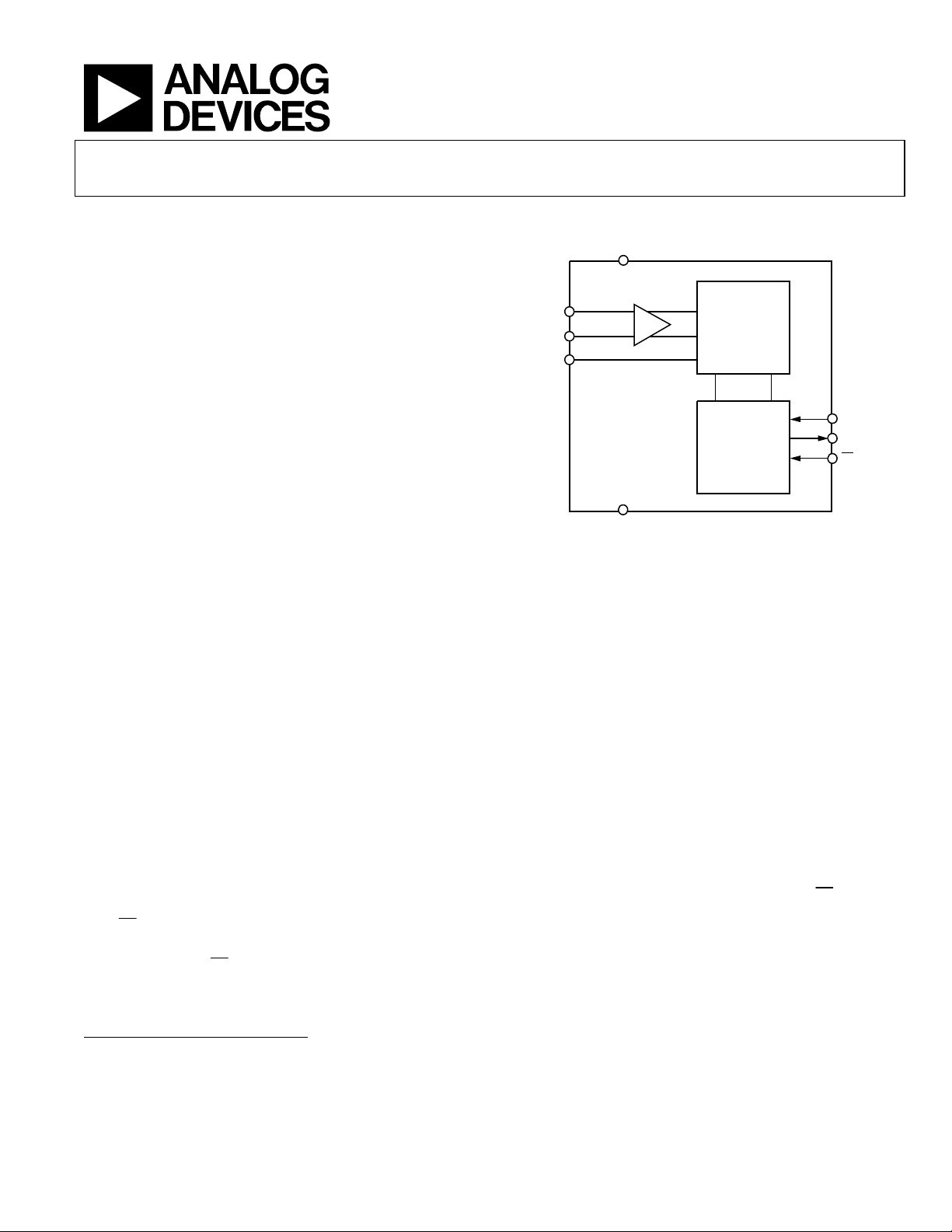
FUNCTIONAL BLOCK DIAGRAM
V
DD
V
IN+
V
IN–
V
REF
AD7441/AD7451
T/H
GND
PRODUCT HIGHLIGHTS
1. Operation with 2.7 V to 5.25 V power supplies.
2. High throughput with low power consumption. With a 3 V
supply, the AD7441/AD7451 offer 4 mW maximum power
consumption for a 1 MSPS throughput rate.
3. Pseudo differential analog input.
4. Flexible power/serial clock speed management. The
conversion rate is determined by the serial clock, allowing
the power to be reduced as the conversion time is reduced
through the serial clock speed increase. These parts also
feature a shutdown mode to maximize power efficiency at
lower throughput rates.
5. Variable voltage reference input.
6. No pipeline delays.
7. Accurate control of the sampling instant via a
once-off conversion control.
8. ENOB > 10 bits typically with 500 mV reference.
One Technology Way, P.O. Box 9106, Norwood, MA 02062-9106, U.S.A.
Tel: 781.329.4700
Fax: 781.326.8703
www.analog.com
© 2005 Analog Devices, Inc. All rights reserved.
12-BIT
SUCCESSIVE
APPROXIMATION
ADC
CONTROL LOGIC
Figure 1.
SCLK
SDATA
CS
CS
input and
03153-A-001

AD7441/AD7451
TABLE OF CONTENTS
AD7451 Specifications..................................................................... 3
Analog Input Structure.............................................................. 14
AD7441 Specifications..................................................................... 5
Timing Specifications....................................................................... 7
Absolute Maximum Ratings............................................................ 8
ESD Caution.................................................................................. 8
Pin Configurations and Function Descriptions ........................... 9
Terminology .................................................................................... 10
Typical Performance Characteristics ........................................... 11
Theory of Operation ...................................................................... 13
Circuit Information.................................................................... 13
Converter Operation.................................................................. 13
ADC Transfer Function............................................................. 13
Typical Connection Diagram ................................................... 14
Analog Input............................................................................... 14
REVISION HISTORY
2/05—Rev. A to Rev. B
Changes to Ordering Guide...............................................................24
Digital Inputs .............................................................................. 15
Reference ..................................................................................... 15
Serial Interface............................................................................ 16
Modes of Operation ....................................................................... 18
Normal Mode.............................................................................. 18
Power-Down Mode.................................................................... 18
Power vs. Throughput Rate....................................................... 20
Microprocessor and DSP Interfacing ...................................... 20
Grounding and Layout Hints.................................................... 22
Evaluating Performance ............................................................ 22
Outline Dimensions....................................................................... 23
Ordering Guide .......................................................................... 24
2/04—Rev. 0 to Rev. A
Updated Format.................................................................... Universal
Changes to General Description .......................................................1
Changes to Table 1 Footnotes ............................................................4
Changes to Table 2 Footnotes ............................................................6
Changes to Table 3 Footnotes ............................................................7
Changes to Table 5 .............................................................................. 9
Updated Figures 7, 8, and 9.............................................................. 13
Changes to Figure 23.........................................................................16
Changes to Reference Section..........................................................17
Rev. B | Page 2 of 24

AD7441/AD7451
AD7451 SPECIFICATIONS
VDD = 2.7 V to 5.25 V; f
versions: −40°C to +85°C.
Table 1.
Parameter Test Conditions/Comments A Version B Version Unit
DYNAMIC PERFORMANCE fIN = 100 kHz
Signal-to-Noise Ratio (SNR)1 VDD = 2.7 V to 5.25 V 70 70 dB min
Signal to (Noise + Distortion) (SINAD)1 VDD = 2.7 V to 3.6 V 69 69 db min
V
Total Harmonic Distortion (THD)1 V
V
Peak Harmonic or Spurious Noise1 V
V
Intermodulation Distortion (IMD)1 fa = 90 kHz; fb = 110 kHz
Second-Order Terms −80 −80 dB typ
Third-Order Terms −80 −80 dB typ
Aperture Delay1 5 5 ns typ
Aperture Jitter1 50 50 ps typ
Full-Power Bandwidth
@ −0.1 dB 2.5 2.5 MHz typ
DC ACCURACY
Resolution 12 12 Bits
Integral Nonlinearity (INL)1 ±1.5 ±1 LSB max
Differential Nonlinearity (DNL)1 Guaranteed no missed codes to 12 bits ±0.95 ±0.95 LSB max
Offset Error1 ±3.5 ±3.5 LSB max
Gain Error1 ±3 ±3 LSB max
ANALOG INPUT
Full-Scale Input Span V
Absolute Input Voltage
V
V
IN+
3
V
VDD = 2.7 V to 3.6 V −0.1 to +0.4 −0.1 to +0.4 V
IN–
V
DC Leakage Current ±1 ±1 µA max
Input Capacitance When in track and hold 30/10 30/10 pF typ
REFERENCE INPUT
V
Input Voltage
REF
DC Leakage Current ±1 ±1 µA max
V
Input Capacitance When in track and hold 10/30 10/30 pF typ
REF
LOGIC INPUTS
Input High Voltage, V
Input Low Voltage, V
Input Current, IIN Typically 10 nA, VIN = 0 V or VDD ±1 ±1 µA max
Input Capacitance, C
LOGIC OUTPUTS
Output High Voltage, VOH VDD = 4.75 V to 5.25 V; I
V
Output Low Voltage, VOL I
Floating-State Leakage Current ±1 ±1 µA max
Floating-State Output Capacitance5 10 10 pF max
Output Coding
= 18 MHz; fS = 1 MSPS; V
SCLK
= 4.75 V to 5.25 V 70 70 dB min
DD
= 2.7 V to 3.6 V; −78 dB typ −73 −73 dB max
DD
= 4.75 V to 5.25 V; −80 dB typ −75 −75 dB max
DD
= 2.7 V to 3.6 V; −80 dB typ −73 −73 dB max
DD
= 4.75 V to 5.25 V; −82 dB typ −75 −75 dB max
DD
1, 2
@ −3 dB 20 20 MHz typ
− V
IN+
= 4.75 V to 5.25 V −0.1 to +1.5 −0.1 to +1.5 V
DD
±1% tolerance for specified
performance
2.4 2.4 V min
INH
0.8 0.8 V max
INL
5
IN
10 10 pF max
= 2.7 V to 3.6 V; I
DD
= 200 µA 0.4 0.4 V max
SINK
= 2.5 V; TA = T
REF
V
IN–
SOURCE
to T
MIN
= 200 µA 2.8 2.8 V min
SOURCE
, unless otherwise noted. Temperature ranges for A, B
MAX
= 200 µA 2.4 2.4 V min
V
REF
V
REF
4
2.54 V
2.5
Straight
(natural) binary
V
REF
V
REF
Straight
(natural) binary
Rev. B | Page 3 of 24

AD7441/AD7451
Parameter Test Conditions/Comments A Version B Version Unit
CONVERSION RATE
Conversion Time 888 ns with an 18 MHz SCLK 16 16 SCLK cycles
Track-and-Hold Acquisition Time1 Sine wave input 250 250 ns max
Full-scale step input 290 290 ns max
Throughput Rate 1 1 MSPS max
POWER REQUIREMENTS
VDD 2.7/5.25 2.7/5.25 V min/max
6, 7
I
DD
Normal Mode (Static) SCLK on or off 0.5 0.5 mA typ
Normal Mode (Operational) VDD = 4.75 V to 5.25 V 1.95 1.95 mA max
V
Full Power-Down Mode SCLK on or off 1 1 µA max
Power Dissipation
Normal Mode (Operational) VDD = 5 V; 1.55 mW typ for 100 ksps6 9.25 9.25 mW max
V
Full Power-Down VDD = 5 V; SCLK on or off 5 5 µW max
V
1
See section. Terminology
2
Analog inputs with slew rates exceeding 27 V/µs (full-scale input sine wave > 3.5 MHz) within the acquisition time could cause the converter to return an incorrect
result.
3
A small dc input is applied to V
4
The AD7451 is functional with a reference input in the range of 100 mV to VDD.
5
Guaranteed by characterization.
6
See the Power vs. Throughput section.
7
Measured with a full-scale dc input.
to provide a pseudo ground for V
IN–
= 2.7 V to 3.6 V 1.45 1.45 mA max
DD
= 3 V; 0.6 mW typ for 100 ksps6 4 4 mW max
DD
= 3 V; SCLK on or off 3 3 µW max
DD
.
IN+
Rev. B | Page 4 of 24

AD7441/AD7451
AD7441 SPECIFICATIONS
VDD = 2.7 V to 5.25 V; f
B version: −40°C to +85°C.
Table 2.
Parameter Test Conditions/Comments B Version Unit
DYNAMIC PERFORMANCE fIN = 100 kHz
Signal to (Noise + Distortion) (SINAD)1 61 dB min
Total Harmonic Distortion (THD)1 2.7 V to 3.6 V; −77 dB typ −72 dB max
4.75 V to 5.25 V; −79 dB typ −73 dB max
Peak Harmonic or Spurious Noise1 2.7 V to 3.6 V; −80 dB typ −72 dB max
4.75 V to 5.25 V; −82 dB typ −74 dB max
Intermodulation Distortion (IMD)
Second-Order Terms −80 dB typ
Third-Order Terms −80 dB typ
Aperture Delay1 5 ns typ
Aperture Jitter1 50 ps typ
Full-Power Bandwidth1, 2 @ −3 dB 20 MHz typ
@ −0.1 dB 2.5 MHz typ
DC ACCURACY
Resolution 10 Bits
Integral Nonlinearity (INL)
Differential Nonlinearity (DNL)1 Guaranteed no missed codes to 10 bits ±0.5 LSB max
Offset Error1 ±1 LSB max
Gain Error1 ±1 LSB max
ANALOG INPUT
Full-Scale Input Span V
Absolute Input Voltage
V
V
IN+
3
V
VDD = 2.7 V to 3.6 V −0.1 to +0.4 V
IN–
V
DC Leakage Current ±1 µA max
Input Capacitance When in track and hold 30/10 pF typ
REFERENCE INPUT
V
Input Voltage
REF
DC Leakage Current ±1 µA max
V
Input Capacitance When in track and hold 10/30 pF typ
REF
LOGIC INPUTS
Input High Voltage, V
Input Low Voltage, V
Input Current, I
IN
Input Capacitance, C
LOGIC OUTPUTS
Output High Voltage, VOH VDD = 4.75 V to 5.25 V ; I
V
Output Low Voltage, VOL I
Floating-State Leakage Current ±1 µA max
Floating-State Output Capacitance5 10 pF max
Output Coding Straight (natural) binary
= 18 MHz; fS = 1 MSPS; V
SCLK
1
1
fa = 90 kHz, fb = 110 kHz
±0.5 LSB max
− V
IN+
= 4.75 V to 5.25 V −0.1 to +1.5 V
DD
±1% tolerance for specified
performance
2.4 V min
INH
0.8 V max
INL
Typically 10 nA, VIN = 0 V or V
5
10 pF max
IN
= 2.7 V to 3.6 V; I
DD
= 200 µA 0.4 V max
SINK
= 2.5 V; TA = T
REF
V
IN–
SOURCE
to T
MIN
DD
= 200 µA 2.8 V min
SOURCE
, unless otherwise noted. Temperature range for
MAX
= 200 µA 2.4 V min
V
REF
V
REF
4
V
2.5
±1 µA max
Rev. B | Page 5 of 24

AD7441/AD7451
Parameter Test Conditions/Comments B Version Unit
CONVERSION RATE
Conversion Time 888 ns with an 18 MHz SCLK 16 SCLK cycles
Track-and-Hold Acquisition Time1 Sine wave input 250 ns max
Step input 290 ns max
Throughput Rate 1 MSPS max
POWER REQUIREMENTS
VDD 2.7/5.25 V min/max
6, 7
I
DD
Normal Mode (Static) SCLK on or off 0.5 mA typ
Normal Mode (Operational) VDD = 4.75 V to 5.25 V 1.95 mA max
V
Full Power-Down Mode SCLK on or off 1 µA max
Power Dissipation
Normal Mode (Operational) VDD = 5 V; 1.55 mW typ for 100 ksps6 9.25 mW max
V
Full Power-Down VDD = 5 V; SCLK on or off 5 µW max
V
1
See the Terminology section.
2
Analog inputs with slew rates exceeding 27 V/µs (full-scale input sine wave > 3.5 MHz) within the acquisition time may cause the converter to return an incorrect
result.
3
A small dc input is applied to V
4
The AD7441 is functional with a reference input in the range 100 mV to VDD.
5
Guaranteed by characterization.
6
See the Power vs. Throughput section.
7
Measured with a full-scale dc input.
to provide a pseudo ground for V
IN–
= 2.7 V to 3.6 V 1.25 mA max
DD
= 3 V; 0.6 mW typ for 100 ksps6 4 mW max
DD
= 3 V; SCLK on or off 3 µW max
DD
.
IN+
Rev. B | Page 6 of 24

AD7441/AD7451
S
A
TIMING SPECIFICATIONS
VDD = 2.7 V to 5.25 V; f
Table 3.
Parameter Limit at T
2
f
10 kHz min
SCLK
t
CONVERT
t
60 ns min
QUIET
18 MHz max
16 × t
888 ns max
t1 10 ns min
t2 10 ns min
3
t
20 ns max
3
t4 40 ns max Data access time after SCLK falling edge
t5 0.4 t
t6 0.4 t
SCLK
SCLK
t7 10 ns min SCLK edge to data valid hold time
4
t
8
t
POWER-UP
10 ns min SCLK falling edge to SDATA three-state enabled
35 ns max SCLK falling edge to SDATA three-state enabled
5
1 µs max Power-up time from full power-down
1
Guaranteed by characterization. All input signals are specified with tr = tf = 5 ns (10% to 90% of VDD) and timed from a voltage level of 1.6 V. See , , and
the section.
Serial Interface
2
Mark/space ratio for the SCLK input is 40/60 to 60/40.
3
Measured with the load circuit of and defined as the time required for the output to cross 0.8 V or 2.4 V with VDD = 5 V and the time required for an output to
cross 0.4 V or 2.0 V for V
4
t8 is derived from the measured time taken by the data outputs to change 0.5 V when loaded with the circuit of Figure 4. The measured number is then extrapolated
back to remove the effects of charging or discharging the 25 pF capacitor. This means that the time, t
time of the part and is independent of the bus loading.
5
See section. Power-Up Time
= 18 MHz; fS = 1 MSPS; V
SCLK
, T
MIN
MAX
SCLK
ns min SCLK high pulse width
ns min SCLK low pulse width
Figure 4
= 3 V.
DD
1
= 2.5 V; TA = T
REF
Unit Description
t
= 1/f
SCLK
SCLK
Minimum quiet time between the end of a serial read and the next falling edge of
Minimum
CS
CS
falling edge to SCLK falling edge set-up time
Delay from
MIN
to T
, unless otherwise noted.
MAX
pulse width
CS
falling edge until SDATA three-state disabled
, quoted in the timing characteristics, is the true bus relinquish
8
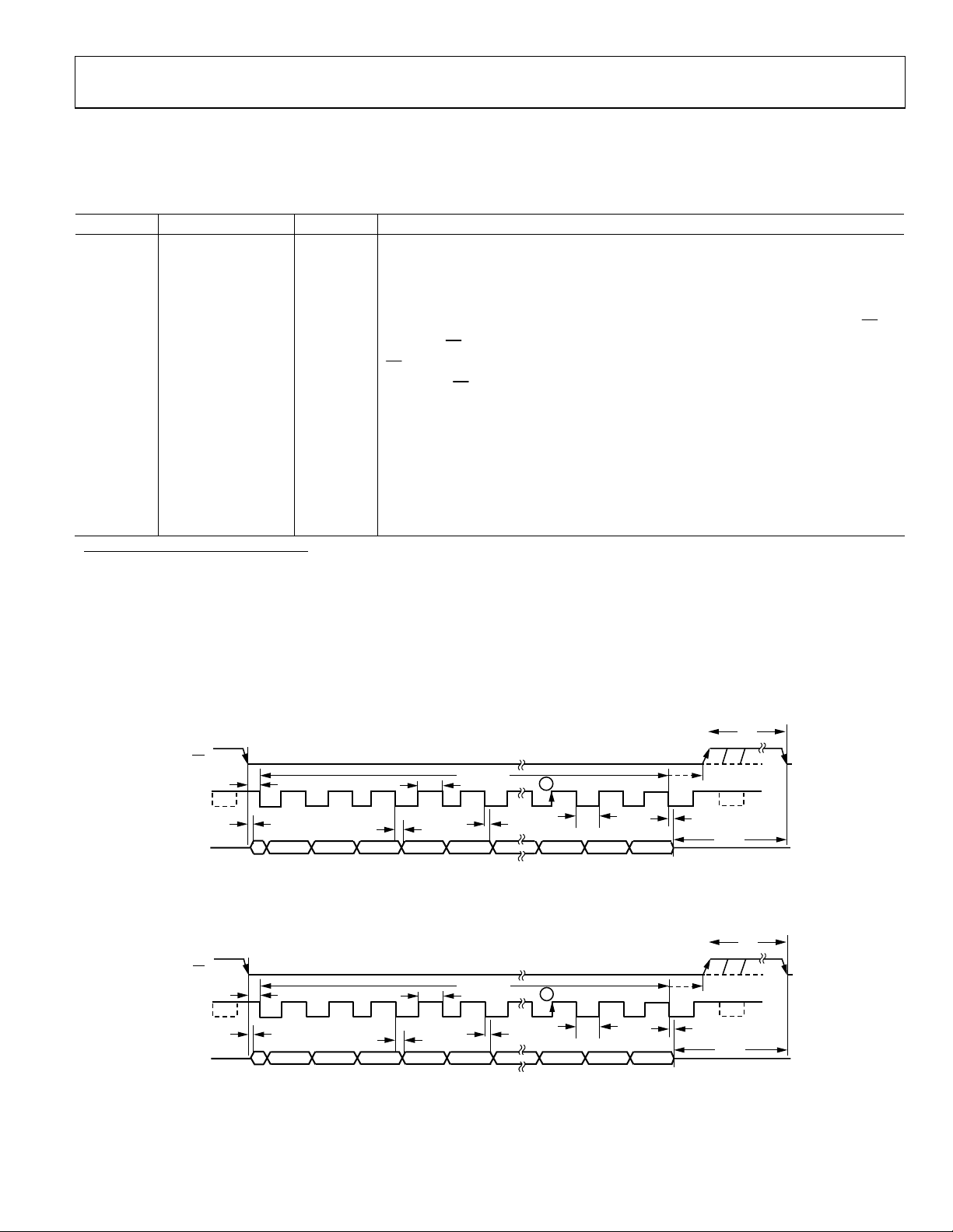
Figure 2 Figure 3
CS
t
1
CS
SCLK
DAT
t
2
12345 13141516
t
3
0 0 0 0 DB11 DB10 DB2 DB1 DB0
4 LEADING ZEROS THREE-STATE
t
4
t
CONVERT
t
5
t
7
B
t
6
t
8
t
QUIET
03153-A-002
Figure 2. AD7451 Serial Interface Timing Diagram
t
1
CS
SCLK
SDATA
t
2
12345 13141516
t
3
0 0 0 0 DB9 DB8 DB0 0 0
4 LEADING ZEROS 2 TRAILING ZEROS
t
4
Figure 3. AD7441 Serial Interface Timing Diagram
t
CONVERT
t
5
t
7
Rev. B | Page 7 of 24
B
t
6
t
8
t
QUIET
THREE-STATE
03153-A-003

AD7441/AD7451
ABSOLUTE MAXIMUM RATINGS
Table 4. TA = 25°C, unless otherwise noted.
Parameter Rating
VDD to GND −0.3 V to +7 V
V
to GND −0.3 V to VDD + 0.3 V
IN+
V
to GND −0.3 V to VDD + 0.3 V
IN–
Digital Input Voltage to GND −0.3 V to +7 V
Digital Output Voltage to GND −0.3 V to VDD + 0.3 V
V
to GND −0.3 V to VDD + 0.3 V
REF
Input Current to any Pin Except Supplies1±10 mA
Operating Temperature Range
−40°C to +85°C
Commercial (A, B Version)
Storage Temperature Range −65°C to +150°C
Junction Temperature 150°C
θJA Thermal Impedance 205.9°C/W (MSOP)
211.5°C/W (SOT-23)
θJC Thermal Impedance 43.74°C/W (MSOP)
Lead Temperature, Soldering
91.99°C/W (SOT-23)
Vapor Phase (60 sec) 215°C
Infrared (15 sec) 220°C
ESD 1 kV
1
Transient currents of up to 100 mA do not cause SCR latch-up.
Stresses above those listed under Absolute Maximum Ratings
may cause permanent damage to the device. This is a stress
rating only; functional operation of the device at these or any
other conditions above those listed in the operational sections
of this specification is not implied. Exposure to absolute
maximum rating conditions for extended periods may affect
device reliability.
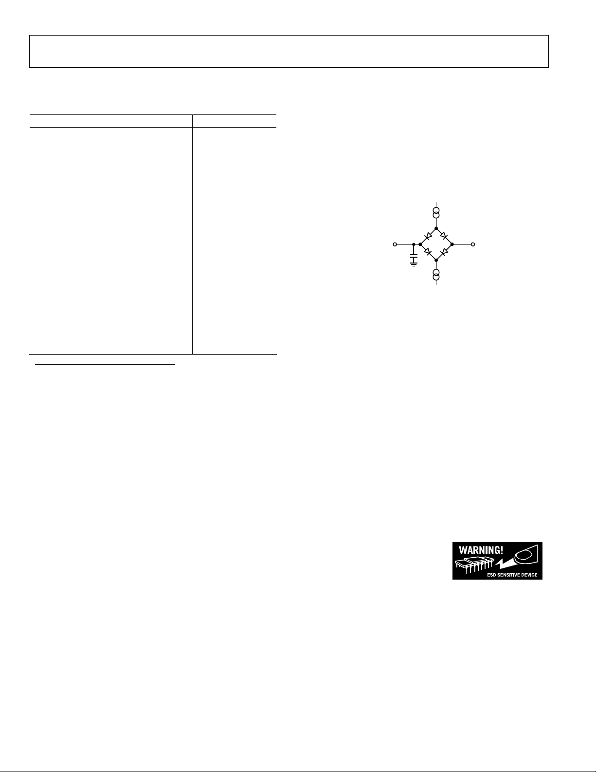
Figure 4. Load Circuit for Digital Output Timing Specifications
TO OUTPUT
PIN
25pF
C
L
1.6mA I
200µAI
OL
OH
1.6V
03153-A-004
ESD CAUTION
ESD (electrostatic discharge) sensitive device. Electrostatic charges as high as 4000 V readily accumulate on
the human body and test equipment and can discharge without detection. Although this product features
proprietary ESD protection circuitry, permanent damage may occur on devices subjected to high energy
electrostatic discharges. Therefore, proper ESD precautions are recommended to avoid performance
degradation or loss of functionality.
Rev. B | Page 8 of 24
 Loading...