Ultralow Noise
BiFET Op Amp
AD743
FEATURES
Ultralow Noise Performance
√
2.9 nV/
Hz at 10 kHz
0.38 V p-p, 0.1 Hz to 10 Hz
6.9 fA/
√
Hz Current Noise at 1 kHz
Excellent DC Performance
0.5 mV Max Offset Voltage
250 pA Max Input Bias Current
1000 V/mV Min Open-Loop Gain
AC Performance
2.8 V/s Slew Rate
4.5 MHz Unity-Gain Bandwidth
THD = 0.0003% @ 1 kHz
Available in Tape and Reel in Accordance with
EIA-481A Standard
APPLICATIONS
Sonar Preamplifiers
High Dynamic Range Filters (>140 dB)
Photodiode and IR Detector Amplifiers
Accelerometers
GENERAL DESCRIPTION
The AD743 is an ultralow noise, precision, FET input, monolithic
operational amplifier. It offers a combination of the ultralow voltage noise generally associated with bipolar input op amps and
the very low input current of a FET input device. Furthermore,
the AD743 does not exhibit an output phase reversal when the
negative common-mode voltage limit is exceeded.
The AD743’s guaranteed, maximum input voltage noise of
4.0 nV/√Hz at 10 kHz is unsurpassed for a FET input monolithic op amp, as is the maximum 1.0 µV p-p, 0.1 Hz to 10 Hz
noise. The AD743 also has excellent dc performance with 250 pA
maximum input bias current and 0.5 mV maximum offset voltage.
The AD743 is specifically designed for use as a preamp in capacitive sensors, such as ceramic hydrophones. The AD743J is rated
over the commercial temperature range of 0°C to 70°C.
The AD743 is available in a 16-lead SOIC and 8-lead PDIP.
PRODUCT HIGHLIGHTS
1. The low offset voltage and low input offset voltage drift of the
AD743 coupled with its ultralow noise performance mean
that the AD743 can be used for upgrading many applications
now using bipolar amplifiers.
CONNECTION DIAGRAMS
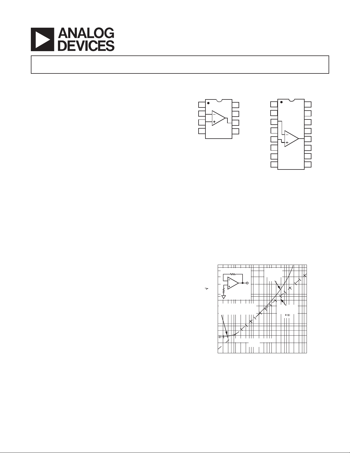
8-Lead PDIP (N) 16-Lead SOIC (R)
NULL
–IN
+IN
–V
1
2
3
4
S
AD743
TOP VIEW
NC = NO CONNECT
1
8
8
NC
+V
7
S
6
OUT
NULL
5
NC
OFFSET
NULL
–IN
NC
+IN
–V
NC
NC
AD743
2
3
4
5
6
S
7
TOP VIEW
8
NC = NO CONNECT
8
16
15
14
13
12
11
10
9
NC
NC
NC
+V
S
OUTPUT
OFFSET
NULL
NC
NC
2. The combination of low voltage and low current noise make
the AD743 ideal for charge sensitive applications such as
accelerometers and hydrophones.
3. The low input offset voltage and low noise level of the AD743
provide >140 dB dynamic range.
4. The typical 10 kHz noise level of 2.9 nV/√Hz permits a three
op amp instrumentation amplifier, using three AD743s, to be
built which exhibits less than 4.2 nV/√Hz noise at 10 kHz
and which has low input bias currents.
1000
)
z
H
/
(nV
E
IS
O
N
E
G
LTA
O
T V
U
P
IN
R
SOURCE
E
O
R
100
SOURCE
AD743 AND RESISTOR
OR
OP27 AND RESISTOR
10
RESISTOR NOISE ONLY
(– – –)
1
100 1k 10k 100k
SOURCE RESISTANCE (⍀)
OP27 AND
RESISTOR
( — )
AD743 AND
RESISTOR
(
)
1M 10M
Figure 1. Input Voltage Noise vs. Source Resistance
REV. E
Information furnished by Analog Devices is believed to be accurate and
reliable. However, no responsibility is assumed by Analog Devices for its
use, nor for any infringements of patents or other rights of third parties that
may result from its use. No license is granted by implication or otherwise
under any patent or patent rights of Analog Devices. Trademarks and
registered trademarks are the property of their respective companies.
One Technology Way, P.O. Box 9106, Norwood, MA 02062-9106, U.S.A.
Tel: 781/329-4700 www.analog.com
Fax: 781/326-8703 © 2003 Analog Devices, Inc. All rights reserved.

AD743–SPECIFICATIONS
(@ 25ⴗC and ⴞ15 V dc, unless otherwise noted.)
Parameter Conditions Min Typ Max Unit
INPUT OFFSET VOLTAGE
1
Initial Offset 0.25 1.0 mV
Initial Offset T
vs. Temperature T
MIN
MIN
to T
to T
vs. Supply (PSRR) 12 V to 18 V
vs. Supply (PSRR) T
INPUT BIAS CURRENT
3
MIN
to T
MAX
MAX
MAX
2
90 96 dB
2 µV/°C
88 dB
1.5 mV
Either Input VCM = 0 V 150 400 pA
Either Input @ T
MAX
Either Input V
VCM = 0 V 8.8 nA
= 10 V 250 600 pA
CM
Either Input, VS = ±5 V VCM = 0 V 30 200 pA
INPUT OFFSET CURRENT V
Offset Current @ T
MAX
= 0 V 40 150 pA
CM
VCM = 0 V 2.2 nA
FREQUENCY RESPONSE
Gain BW, Small Signal G = –1 4.5 MHz
Full Power Response V
= 20 V p-p 25 kHz
O
Slew Rate, Unity Gain G = –1 2.8 V/µs
Settling Time to 0.01% 6 µs
Total Harmonic Distortion
4
f = 1 kHz
(TPC 16) G = –1 0.0003 %
INPUT IMPEDANCE
Differential 1 10
10
储20 Ω储pF
Common Mode 3 1011储18 Ω储pF
INPUT VOLTAGE RANGE
Differential
Common-Mode Voltage +13.3, –10.7 V
Over Maximum Operating Range
Common-Mode Rejection Ratio V
5
6
= ±10 V 80 95 dB
CM
T
to T
MIN
MAX
–10 +12 V
78 dB
±20 V
INPUT VOLTAGE NOISE 0.1 Hz to 10 Hz 0.38 µV p-p
f = 10 Hz 5.5 nV/√Hz
f = 100 Hz 3.6 nV/√Hz
f = 1 kHz 3.2 5.0 nV/√Hz
f = 10 kHz 2.9 4.0 nV/√Hz
INPUT CURRENT NOISE f = 1 kHz 6.9 fA/√Hz
OPEN-LOOP GAIN V
= ±10 V,
O
≥ 2 kΩ 1000 4000 V/mV
R
LOAD
to T
T
R
MIN
LOAD
MAX
= 600 Ω 1200 V/mV
800 V/mV
OUTPUT CHARACTERISTICS
Voltage R
≥ 600 Ω +13, –12 V
LOAD
≥ 600 Ω +13.6, –12.6 V
R
LOAD
to T
T
R
MIN
LOAD
MAX
≥ 2 kΩ±12 +13.8, –13.1 V
+12, –10 V
Current Short Circuit 20 40 mA
POWER SUPPLY
Rated Performance ±15 V
Operating Range ±4.8 ± 18 V
Quiescent Current 8.1 10.0 mA
TRANSISTOR COUNT No. of Transistors 50
NOTES
1
Input offset voltage specifications are guaranteed after five minutes of operation at TA = 25°C.
2
Test conditions: +VS = 15 V, –VS = 12 V to 18 V; and +VS = 12 V to 18 V, –VS = 15 V.
3
Bias current specifications are guaranteed maximum at either input after 5 minutes of operation at TA = 25°C. For higher temperature, the current doubles every 10°C.
4
Gain = –1, RL = 2 kΩ, CL = 10 pF.
5
Defined as voltage between inputs, such that neither exceeds ±10 V from common.
6
The AD743 does not exhibit an output phase reversal when the negative common-mode limit is exceeded.
All min and max specifications are guaranteed.
Specifications subject to change without notice.
REV. E–2–

AD743
ABSOLUTE MAXIMUM RATINGS
Supply Voltage . . . . . . . . . . . . . . . . . . . . . . . . . . . . . . . . ±18 V
Internal Power Dissipation
2
Input Voltage . . . . . . . . . . . . . . . . . . . . . . . . . . . . . . . . . . . ±V
Output Short Circuit Duration . . . . . . . . . . . . . . . . Indefinite
Differential Input Voltage . . . . . . . . . . . . . . . . . . +V
Storage Temperature Range (N, R) . . . . . . . –65°C to +125°C
Operating Temperature Range
AD743J . . . . . . . . . . . . . . . . . . . . . . . . . . . . . . . 0°C to 70°C
Lead Temperature Range (Soldering 60 sec) . . . . . . . . . 300°C
NOTES
1
Stresses above those listed under Absolute Maximum Ratings may cause permanent damage to the device. This is a stress rating only; and functional operation
of the device at these or any other conditions above those indicated in the
operational section of this specification is not implied. Exposure to absolute
maximum rating conditions for extended periods may affect device reliability.
2
8-lead PDIP: JA = 100°C/W, JC = 30°C/W.
16-lead SOIC: JA = 100°C/W, JC = 30°C/W.
1
ORDERING GUIDE
Temperature Package
Model Range Option*
S
AD743JN 0°C to 70°C N-8
and –V
S
S
AD743JR-16 0°C to 70°C R-16
AD743JR-16-REEL 0°C to 70°CTape and Reel
AD743JR-16-REEL7 0°C to 70°CTape and Reel
*N = PDIP; R = SOIC.
ESD SUSCEPTIBILITY
An ESD classification per method 3015.6 of MIL-STD-883C has
been performed on the AD743. The AD743 is a Class 1 device,
passing at 1000 V and failing at 1500 V on null Pins 1 and 5,
when tested, using an IMCS 5000 automated ESD tester. Pins
other than null pins fail at greater than 2500 V.
CAUTION
ESD (electrostatic discharge) sensitive device. Electrostatic charges as high as 4000 V readily
accumulate on the human body and test equipment and can discharge without detection. Although the
AD743 features proprietary ESD protection circuitry, permanent damage may occur on devices
subjected to high energy electrostatic discharges. Therefore, proper ESD precautions are recommended
to avoid performance degradation or loss of functionality.
REV. E
–3–

AD743–Typical Performance Characteristics
0
(ⴞV)
0
k
(Hz)
0
(@ 25ⴗC, VS = 15 V)
20
R
= 10k⍀
LOAD
15
10
5
INPUT VOLTAGE SWING (V)
0
0510
SUPPLY VOLTAGE (ⴞV)
+V
IN
–V
IN
15 2
TPC 1. Input Voltage Swing vs.
Supply Voltage
12
9
6
3
QUIESCENT CURRENT (mA)
20
R
= 10k⍀
LOAD
15
10
50
OUTPUT VOLTAGE SWING (V)
0
0510
POSITIVE
SUPPLY
NEGATIVE
SUPPLY
SUPPLY VOLTAGE (ⴞV)
TPC 2. Output Voltage Swing
vs. Supply Voltage
–6
10
–7
10
–8
10
–9
10
–10
10
INPUT BIAS CURRENT (A)
–11
10
15 20
35
30
25
20
15
10
5
OUTPUT VOLTAGE SWING (V p-p)
0
10 100 1k
LOAD RESISTANCE (⍀)
TPC 3. Output Voltage Swing
vs. Load Resistance
200
100
10
1
0.1
OUTPUT IMPEDANCE (⍀)
10
0
0510
SUPPLY VOLTAGE
15 20
TPC 4. Quiescent Current vs.
Supply Voltage
300
200
100
INPUT BIAS CURRENT (pA)
0
–12 –9 3 6 9 12–6
–3 0
COMMON-MODE VOLTAGE (V)
TPC 7. Input Bias Current vs.
Common-Mode Voltage
–12
10
–60 –40 –20 0 20 40 60 80 100 120 140
TEMPERATURE (ⴗC)
TPC 5. Input Bias Current vs.
Temperature
80
70
60
50
40
30
CURRENT LIMIT (mA)
20
10
0
–60 –40 –20 0 20 40 60 80 100 120 14
+ OUTPUT
CURRENT
– OUTPUT
CURRENT
TEMPERATURE (ⴗC)
TPC 8. Short Circuit Current
Limit vs. Temperature
0.01
10k 100k 1M
FREQUENCY
10M 100M
TPC 6. Output Impedance vs.
Frequency (Closed-Loop Gain = –1)
7.0
6.0
5.0
4.0
3.0
GAIN BANDWIDTH PRODUCT (MHz)
2.0
–60 –40 –20 0 20 40 60 80 100 120 14
TEMPERATURE (ⴗC)
TPC 9. Gain Bandwidth Product
vs. Temperature
REV. E–4–
 Loading...