Low Cost, Low Power
=
Preliminary Technical Data
FEATURES
2.5V Stereo Audio Codec with 3.3 V Tolerant Digital
Interface
Supports 96 kHz Sample Rates
Supports 16/18 /20/24-Bit Word Lengths
Multibit Sigma Delta Modulators with
“Perfect Differential Linearity Restoration” for
Reduced Idle Tones and Noise Floor
Data Directed Scrambling DACs - Least Sensitive to Jitter
Performance (20 Hz to 20 kHz)
90 dB ADC and DAC SNR
Digitally Programmable Input/Output Gain
On-chip Volume Controls Per Output Channel
Hardware and Software Controllable Clickless Mute
Supports 256xFs, 512xF
Master Clock Pre-Scaler for use with DSP master clocks
Flexible Serial Data Port with Right-Justified, LeftJustified, I
2
S-Compatible and DSP Serial Port Modes
Supports Packed Data Mode (“TDM”) for cascading
devices.
On-Chip Reference
16, 20 and 24-Lead SOIC, SSOP and TSSOP Package
options.
APPLICATIONS
Digital Video Camcorders (DVC)
Portable Audio Devices (Walkman etc)
Audio Processing
Voice Processing
Conference Phones
General Purpose Analog I/O
and 768xFs Master Mode Clocks
s
PRELIMINARY
TECHNICAL
Stereo Audio Analog Front End
DVDD1(EXT)
CDIN
CDOUT
CCLK
CLATCH
ASDATA/SDO
DSDATA/SDI
LRCLK/SDIFS
SDOFS
BCLK/SCLK
CDIN
CDOUT
CCLK
CLATCH
ASDATA
DATA
DSDATA
LRCLK
BCLK
SPI
Port
I2S
Port
DGND
DVDD1(EXT)
SPI
Port
I2S
Port
AD74322
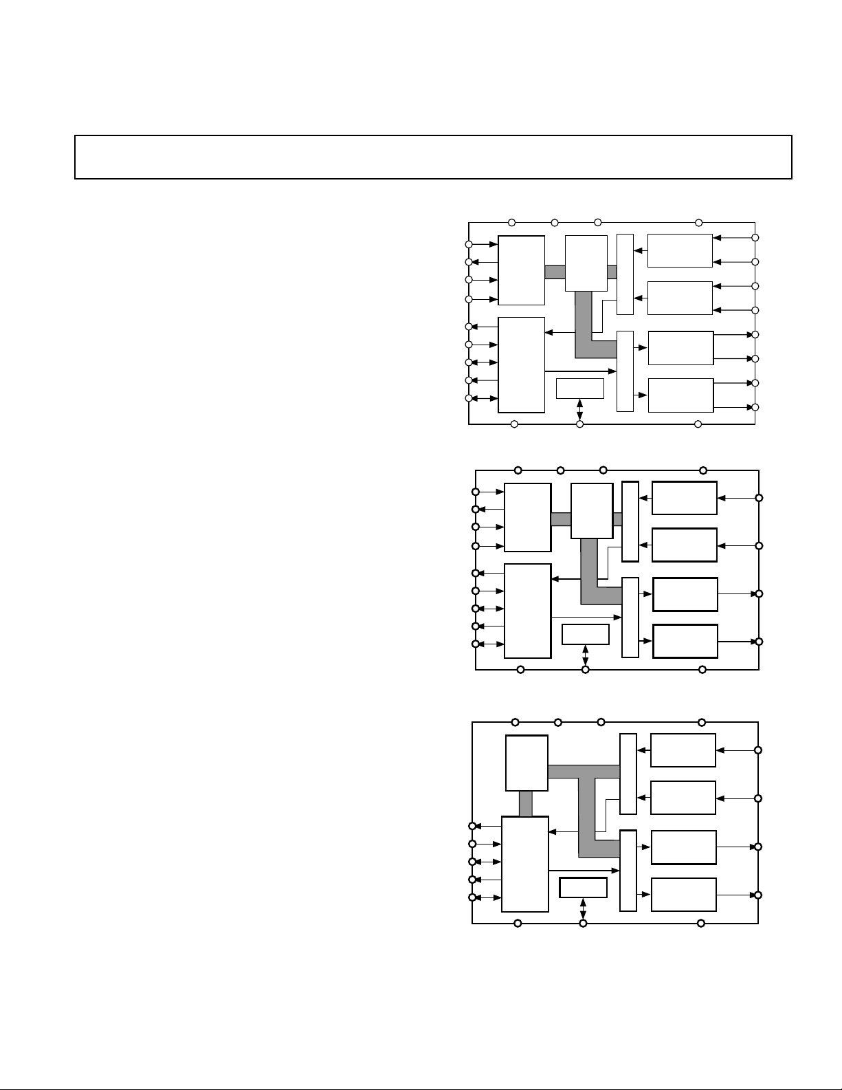
FUNCTIONAL BLOCK DIAGRAM
CLKINDVDD2(INT)
Control
Block
Reference
CLKINDVDD2(INT)
Control
Block
Reference
AVDD
ADC
CHANNEL 1
ADC
CHANNEL 2
DAC
CHANNEL 1
DAC
CHANNEL 2
AGNDREFCAP
AVDD
ADC
CHANNEL 1
ADC
CHANNEL 2
DAC
CHANNEL 1
DAC
CHANNEL 2
VIN1P
VIN1N
VIN2P
VIN2N
VOUT1P
VOUT1N
VOUT2P
VOUT2N
VIN1
VIN2
VOUT1
VOUT2
GENERAL DESCRIPTION
The AD74322 is a front-end processor for general purpose
audio and voice applications. It features two multi-bit Σ∆
A/D conversion channels and two multi-bit Σ∆ D/A
conversion channels. Each ADC channel provides >85 dB
signal-to-noise ratio while each DAC channel provides
>90 dB, both over an audio signal bandwidth.
The AD74322 is particularly suitable for a variety of applications where stereo input and output channels are
required, including audio sections of Digital Video
Camcorder, portable personal audio devices and the
analog front ends of conference phones . Its high quality
performance also make it suitable for speech and telephony
applications such as speech recognition and synthesis and
modern feature phones.
REV. Pr D 03/00
Information furnished by Analog Devices is believed to be accurate and
reliable. However, no responsibility is assumed by Analog Devices for its
use, nor for any infringements of patents or other rights of third parties
which may result from its use. No license is granted by implication or
otherwise under any patent or patent rights of Analog Devices.
DGND
DVDD1(EXT)
Control
Block
SDO
SDI
SDIFS
SDOFS
SCLK
One T echnolog y Way, P .O . Box 91 06, Norwood, MA 02062-9106, U.S.A.
T e l: 781/329-4700 World Wide W eb Site: http://www .analog.com
Fax: 781/326-8703 Analog Devices, Inc., 1998
Data
Port
DGND
CLKINDVDD2(INT)
Reference
AGNDREFCAP
AVDD
ADC
CHANNEL 1
ADC
CHANNEL 2
DAC
CHANNEL 1
DAC
CHANNEL 2
AGNDREFCAP
VIN1
VIN2
VOUT1
VOUT2

AD74322
An on-chip reference voltage is included but can be
bypassed if required for use with an external reference
source.
The AD74322 offers sampling rates which, depending on
MCLK selection and MCLK divider ratio, range from 8
kHz in the voiceband range to 96 kHz in the audio range.
The digital interface to the AD74322 is configured as two
separate ports which allow separation of device control
and data streams. Control and status are monitored using
®
an SPI
data streams are controlled using an I
2
I
Left/Right Clock pins. There is also a DSP mode
available on the audio data port which will also allow both
control and data to be streamed through the same interface
where controller resources are limited.
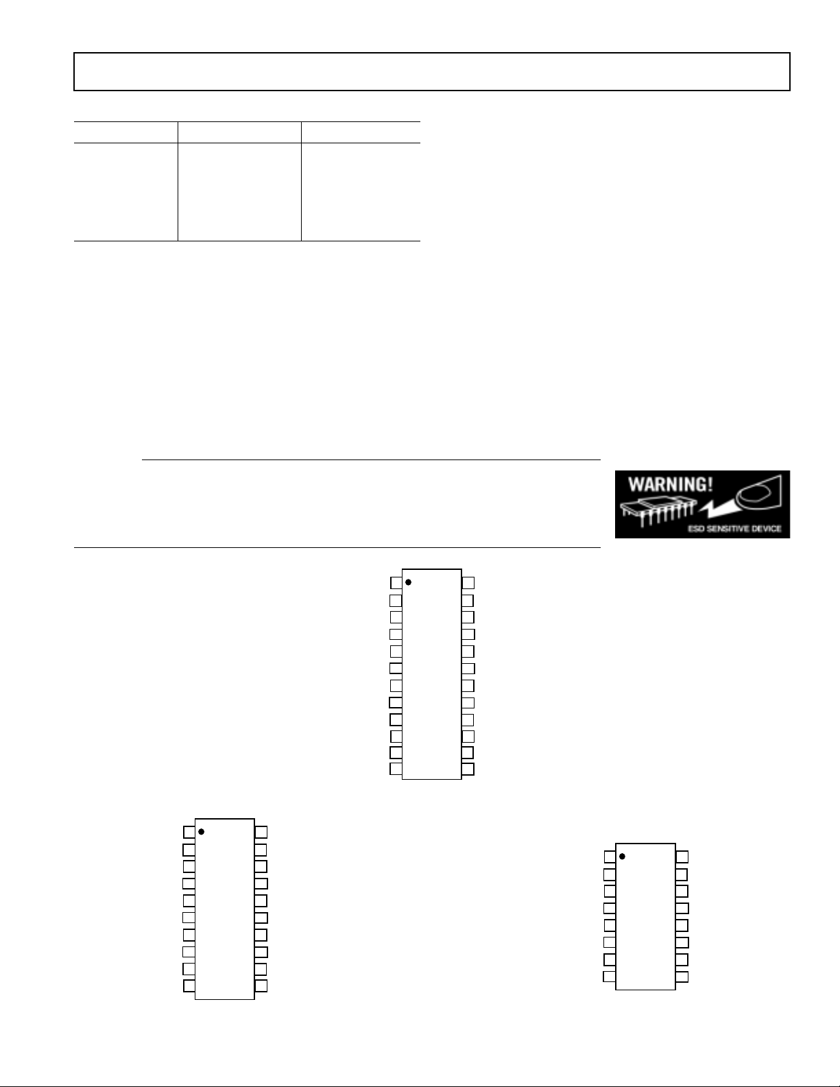
The AD74322 is available in various lead count package
options. These range from a 16-pin variant with singleended inputs/outputs and no SPI port through a 20-pin
variant with single-ended inputs/outputs and an SPI port
to a 24-pin variant with differential inputs/outputs and an
SPI port. These devices will be available in SOIC, SSOP
and TSSOP package options and are specified for the
industrial temperature range of -40°C to +85°C.
compatible serial port while the input and output
S streams are controlled by a common Bit-Clock and
2S®
port. The two
PRELIMINARY TECHNICAL DA TA
PRELIMINARY
TECHNICAL
DATA
– 2 – Pr D 03/00

PRELIMINARY TECHNICAL DA TA
AD74322A
PARAMETER Min Ty p Max Units Test Conditions
ANALOG-TO-DIGITAL CONVERTERS
ADC Resolution (all ADCs) 24 Bits
Dynamic Range (20 Hz to 20 kHz, -60 dB Input)
No Filter 9 0 d B
With A-Weighted Filter 9 2 d B
Total Harmonic Distortion + Noise -85(0.0056) dB(%)
Interchannel Isolation TBD d B
Interchannel Gain Mismatch TBD d B
Programmable Input Gain 12 dB
Gain Step Size 3 d B
Offset Error 0 LSB
Full Scale Input Voltage At Each Pin 0.5 (1.414) Vrms (Vpp) Single Ended
Automatic Level Control
Attack Time Resolution TBD Bits
Attack Time T BD µs/Bit
Decay Time Resolution TBD Bits
Decay Time TB D µs/Bit
Gain Drift TBD ppm/°C
Input Resistance 10 kΩ
Input Capacitance 15 p F
Common Mode Input Volts 1.1V V
DIGITAL-TO-ANALOG CONVERTERS
Dynamic Range (20 Hz to 20 kHz, -60 dB Input)
No Filter 9 0 d B
With A-Weighted Filter 9 2 d B
Total Harmonic Distortion + Noise -85(0.0056) dB(%)
Interchannel Isolation TBD d B
Interchannel Gain Mismatch TBD dB(%)
DC Accuracy
Gain Error T B D %
Interchannel Gain Mismatch TBD ppm/°C
Gain Drift T BD d B
Interchannel Crosstalk (EIAJ method) TBD d B
Interchannel Phase Deviation TBD Degrees
Volume Control Step Size (1023 Linear Steps) 0.098 %
Volume Control Range (Max Attenuation) 60 dB
Mute Attenuation -100 d B
De-emphasis Gain Error +/- 0.1 d B
Full Scale Output Voltage At Each Pin 0.5 (1.414) Vrms(Vpp) Single Ended
Output Resistance At Each Pin ?? ?? Ω
Common Mode Output Volts 2.25 V
REFERENCE (Internal)
Absolute Voltage, V
V
TC T BD ppm/°C
REF
ADC DECIMATION FILTER
Pass Band 0.xxxFs Hz
Pass Band Ripple ±0.00xx d B
Transition Band 0.xxFs 0.xxFs Hz
Stop Band 0.xxFs H z
Stop Band Attenuation 7 0 d B
Group Delay lll/Fs nnn/Fs mmm/Fs m s
DAC INTERPOLATION FILTER
Pass Band 0.xxxFs Hz
Pass Band Ripple ±0.00xx d B
Transition Band 0.xxFs 0.xxFs Hz
Stop Band 0.xxFs H z
Stop Band Attenuation 7 0 d B
Group Delay lll/Fs nnn/Fs mmm/Fs m s
PR D 03/00
REF
PRELIMINARY
TECHNICAL
DATA
1.1 V
–3–
AD74322

AD74322–SPECIFICA TIONS
PARAMETER Min Typ Max Units Test Conditions
LOGIC INPUT
V
, Input High Voltage DVDD1 - 0.8 DVDD1 V
INH
, Input Low Voltage 0 0. 8 V
V
INL
Input Current -10 +10 µA
Input Capacitance 10 p F
LOGIC OUTPUT
VOH, Output High Voltage DVDD1 - 0.4 DVDD1 V
, Output Low Voltage 0 0.4 V
V
OL
Three-State Leakage Current -10 +10 µA
POWER SUPPLIES
AVDD, DVDD2 2.25 2.5 2.75 V
DVDD1 2.7 3.0 3.3 V
POWER CONSUMPTION
All Sections On TBD m A
ADCs On Only TB D mA
DACs On Only TB D mA
Reference On Only TBD m A
Powerdown Mode TBD µA
(AVDD = DVDD2 = +2.5V ±10%, DVDD1 = 3.0V ±10%, f
f
= 48 kHz, TA = T
SAMP
AD74322A
MIN
to T
, unless otherwise noted)
MAX
CLKIN
= 12.288 MHz,
PRELIMINARY
TECHNICAL
DATA
–4–
Pr D 03/00

PRELIMINARY TECHNICAL DA TA
ORDERING GUIDE
Model Range Package
AD74322DAR -40 C to +85 C R-16
AD74322DARU -40 C to +85 C RU-16
AD74322AAR -40 C to +85 C R-20
AD74322AARU -40 C to +85 C RU-20
AD74322AAR -40 C to +85 C R-24
AD74322AARU -40 C to +85 C RU-24
CAUTION
ESD (electrostatic discharge) sensitive device. Electrostatic charges as high as 4000 V readily
accumulate on the human body and test equipment and can discharge without detection.
Although the XX0000 features proprietary ESD protection circuitr y, permanent damage may
occur on devices subjected to high energy electrostatic discharges. Therefore, proper ESD
precautions are recommended to avoid performance degradation or loss of functionality.
PRELIMINARY
AD74322
VOUTP2VINP2
1
VINP1
VINP1
2
3
AGND
4
DGND
5
DVDD2
6
CIN
TOP VIEW
7
(Not to Scale)
8
9
10
DVDD1
MCLK SCLK
CCLK
20
19
18
17
16
15
14
13
12
11
VOUTP1
VOUTP1
AVDDREFCAP
RESET
SDO
SDFS
SDI
COUT
CLATCH
TECHNICAL
VINN1
1
VINN2
VINP1
AGND
DGND
DVDD2
DVDD1
MCLK SCLK
CCLK
CIN
DATA
2
3
4
5
6
7
8
TOP VIEW
9
(Not to Scale)
10
11
12
24
23
22
21
20
19
18
17
16
15
14
13
VOUTN1
VOUTN2
VOUTN1VINN1
VOUTP1
AVDDREFCAP
RESET
SDO
SDFS
SDI
COUT
CLATCH
1
VINP1
VINP1
2
3
AGND
4
DGND
5
DVDD2
6
DVDD1
7
MCLK SCLK
8
TOP VIEW
(Not to Scale)
16
15
14
13
12
11
10
9
VOUTP2VINP2
VOUTP1
VOUTP1
AVDDREFCAP
RESET
SDO
SDFS
SDI
–5–Pr D 03/00

AD74322
PIN FUNCTION DESCRIPTION (SINGLE-ENDED I/O ; NO SPI PORT)
Mnemonic I/O Function
VIN1 I Analog Input - Channel 1
VIN2 I Analog Input - Channel 2
VOUT1 O Analog Output - Channel 1
VOUT2 O Analog Output - Channel 2
REFCAP I/O Internal Reference - Can also be used for connection of an external reference
AVDD Analog Power Supply Connection
AGND Analog Ground/Substrate Connection
DVDD1 Digital Power Supply Connection (Interface)
DVDD2 Digital Power Supply Connection (Core)
DGND Digital Ground/Substrate Connection
MCLK I External Clock Connection
SDO O ADC Serial Data Out - DSP Mode
SDI I DAC Serial Data In - DSP Mode
SDFS I/O Serial Data Input Frame Sync - DSP Mode
4-5-6 I Powerdown/Reset Input
SCLK I/O Serial Clock - DSP Mode
PIN FUNCTION DESCRIPTION (SINGLE-ENDED I/O WITH SPI PORT)
Mnemonic I/O Function
VIN1 I Analog Input - Channel 1
VIN2 I Analog Input - Channel 2
VOUT1 O Analog Output - Channel 1
VOUT2 O Analog Output - Channel 2
REFCAP I/O Internal Reference - Can also be used for connection of an external reference
AVDD Analog Power Supply Connection
AGND Analog Ground/Substrate Connection
DVDD1 Digital Power Supply Connection (Interface)
DVDD2 Digital Power Supply Connection (Core)
DGND Digital Ground/Substrate Connection
MCLK I External Clock Connection
CDIN I Serial Data In on SPI Control Port
CDOUT O Serial Data Out on SPI Control Port
CCLK I Serial Clock on SPI Control Port
CLATCH I Serial Data Latch on SPI Control Port
ASDATA O ADC Serial Data Out - I
DSDATA I DAC Serial Data In - I
LRCLK/ I/O Left/Right Channel Select - I
BCLK I/O Bit Clock - I
RESET I Powerdown/Reset Input
PRELIMINARY
TECHNICAL
DATA
2
S
2
S
2
S
2
S
PRELIMINARY TECHNICAL DA TA
– 6 – Pr D 03/00
 Loading...