查询AD7416-7418供应商
10-Bit Digital Temperature Sensor (AD7416) and
Four Single-Channel ADCs (AD7417/AD7418)
AD7416/AD7417/AD7418
FEATURES
10-Bit ADC with 15 s and 30 s Conversion Times
Single and Four Single-Ended Analog Input Channels
On-Chip Temperature Sensor: –40ⴗC to +125ⴗC
On-Chip Track-and-Hold
Overtemperature Indicator
Automatic Power-Down at the End of a Conversion
Wide Operating Supply Range: 2.7 V to 5.5 V
2C®
Compatible Serial Interface
I
Selectable Serial Bus Address Allows Connection of up
to Eight AD7416/AD7417s to a Single Bus
AD7416 Is a Superior Replacement for LM75
APPLICATIONS
Data Acquisition with Ambient Temperature Monitoring
Industrial Process Control
Automotive
Battery-Charging Applications
Personal Computers
GENERAL DESCRIPTION
The AD7417 and AD7418 are 10-bit, 4-channel and singlechannel ADCs with an on-chip temperature sensor that
can operate from a single 2.7 V to 5.5 V power supply. The
devices contain a 15 µs successive approximation converter, a
5-channel multiplexer, a temperature sensor, a clock oscillator, a track-and-hold, and a reference (2.5 V). The AD7416
is a temperature-monitoring only device in an 8-lead package.
The temperature sensor on the parts can be accessed via multiplexer Channel 0. When Channel 0 is selected and a conversion
is initiated, the resulting ADC code at the end of the conversion
gives a measurement of the ambient temperature (±1°C @ 25°C).
On-chip registers can be programmed with high and low temperature limits, and an open-drain overtemperature indicator
(OTI) output is provided, which becomes active when a programmed limit is exceeded.
A configuration register allows programming of the sense of the
OTI output (active high or active low) and its operating mode
(comparator or interrupt). A programmable fault queue counter
allows the number of out-of-limit measurements that must occur
before triggering the OTI output to be set to prevent spurious
triggering of the OTI output in noisy environments.
(continued on page 7)
ADDRESS
REGISTER
A0
A1
A2
A
IN1
A
IN2
A
IN3
A
IN4
NC = NO CONNECT
A
IN1
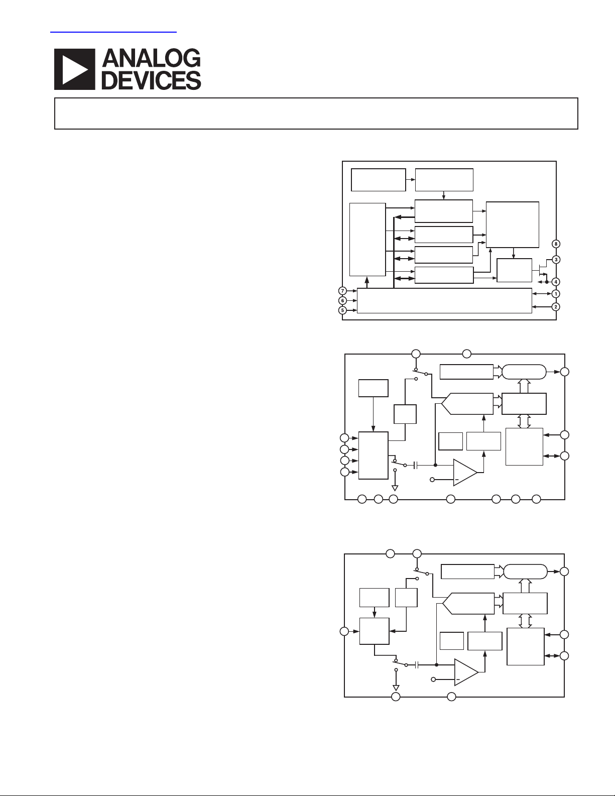
FUNCTIONAL BLOCK DIAGRAMS
BAND GAP
TEMPERATURE
SENSOR
POINTER
TEMP
SENSOR
MUX
NC NC GND
V
DD
TEMP
SENSOR
MUX
REF
2.5V
SAMPLING
CAPACITOR
REF
2.5V
SAMPLING
CAPACITOR
10-BIT
ANALOG-DIGITAL
CONVERTER
TEMPERATURE
VALUE
REGISTER
T
SETPOINT
OTI
REGISTER
T
SETPOINT
HYST
REGISTER
CONFIGURATION
REGISTER
SERIAL BUS
INTERFACE
REF
IN
OVERTEMP REG
CLOCK
V
BALANCE
CONVST
REF
IN
OVERTEMP REG
CLOCK
V
DD
CHARGE
DISTRIBUTION
DAC
CONTROL
LOGIC
+
CHARGE
DISTRIBUTION
DAC
CONTROL
LOGIC
+
COMPARATOR
AD7416
SETPOINT
FAULT
QUEUE
COUNTER
A > B
B
DATA OUT
INTERFACE
AD7417
B
DATA OUT
INTERFACE
A
I2C
A > B
A
I2C
V
DD
OTI
GND
SDA
SCL
OTI
SCL
SDA
A2A1A0
OTI
SCL
SDA
REV. G
Information furnished by Analog Devices is believed to be accurate and
reliable. However, no responsibility is assumed by Analog Devices for its
use, nor for any infringements of patents or other rights of third parties that
may result from its use. No license is granted by implication or otherwise
under any patent or patent rights of Analog Devices. Trademarks and
registered trademarks are the property of their respective owners.
AD7418
GND
V
BALANCE
CONVST
One Technology Way, P.O. Box 9106, Norwood, MA 02062-9106, U.S.A.
Tel: 781/329-4700 www.analog.com
Fax: 781/326-8703 © 2004 Analog Devices, Inc. All rights reserved.

AD7416/AD7417/AD7418
AD7417/AD7418–SPECIFICATIONS
(VDD = 2.7 V to 5.5 V, GND = 0 V, REFIN = 2.5 V, unless otherwise noted.)
Parameter A Version B Version1Unit Test Conditions/Comments
DC ACCURACY Any Channel.
Resolution 10 10 Bits
Minimum Resolution for Which No
Missing Codes Are Guaranteed 10 10 Bits
Relative Accuracy
Differential Nonlinearity
Gain Error
Gain Error Match
Offset Error
2
2
2
2
2
± 1 ±1LSB max This Specification Is Typical for VDD of
3.6 V to 5.5 V.
± 1 ±1LSB max This Specification Is Typical for VDD of
3.6 V to 5.5 V.
± 3 ±3LSB max External Reference.
± 10 ± 10 LSB max Internal Reference.
± 0.6 ± 0.6 LSB max AD7417 Only.
± 4 ±4LSB max
Offset Error Match ± 0.7 ± 0.7 LSB max AD7417 Only.
ANALOG INPUTS
Input Voltage Range V
Input Leakage Current
3
REF
00 V min
± 1 ±1 µA max
V
REF
V max
Input Capacitance 10 10 pF max
TEMPERATURE SENSOR
1
Measurement Error
Ambient Temperature 25°C ± 2 ±1 °C max
to T
T
MIN
MAX
± 3 ±2 °C max
Temperature Resolution 1/4 1/4 °C/LSB
CONVERSION RATE
Track-and-Hold Acquisition Time
4
400 400 ns max Source Impedance < 10 Ω.
Conversion Time
Temperature Sensor 30 30 µs max Typically 27 µs.
Channels 1 to 4 15 15 µs max Typically 10 µs.
REFERENCE INPUT
REFIN Input Voltage Range
5, 6
6
2.625 2.625 V max 2.5 V + 5%.
2.375 2.375 V min 2.5 V – 5%.
Input Impedance 40 40 kΩ min
Input Capacitance 10 10 pF max
ON-CHIP REFERENCE Nominal 2.5 V.
Reference Error
Temperature Coefficient
6
6
± 25 ± 25 mV max
80 80 ppm/°C typ
DIGITAL INPUTS
Input High Voltage, V
Input Low Voltage, V
IL
IH
VDD × 0.7 VDD × 0.7 V min
VDD × 0.3 VDD × 0.3 V max
Input Leakage Current 1 1 µA max
DIGITAL OUTPUTS
Output Low Voltage, V
OL
0.4 0.4 V max IOL = 3 mA.
Output High Current 1 1 µA max VOH = 5 V.
POWER REQUIREMENTS
V
DD
5.5 5.5 V max For Specified Performance.
2.7 2.7 V min
I
DD
Logic Inputs = 0 V or V
DD.
Normal Operation 600 600 µA max
Power-Down 1 1 µA max 50 nA Typically.
Auto Power-Down Mode V
= 3 V. See Operating Modes.
DD
10 SPS Throughput Rate 6 6 µW typ
1 kSPS Throughput Rate 60 60 µW typ
10 kSPS Throughput Rate 600 600 µW typ
Power-Down 3 3 µW max Typically 0.15 µW.
REV. G–2–

AD7416/AD7417/AD7418
NOTES
1
B Version applies to AD7417 only with temperature range of –40°C to +85°C. A Version temperature range is –40°C to +125°C. For VDD = 2.7 V, TA = 85°C max
and temperature sensor measurement error = ± 3°C.
2
See Terminology.
3
Refers to the input current when the part is not converting. Primarily due to reverse leakage current in the ESD protection diodes.
4
Sample tested during initial release and after any redesign or process change that may affect this parameter.
5
On-chip reference shuts down when external reference is applied.
6
The accuracy of the temperature sensor is affected by reference tolerance. The relationship between the two is explained in the Temperature Sensor section.
Specifications subject to change without notice.
AD7416–SPECIFICATIONS
(VDD = 2.7 V to 5.5 V, GND = 0 V, REFIN = 2.5 V, unless otherwise noted.)
Parameter Min Typ Max Unit Test Conditions/Comments
TEMPERATURE SENSOR AND ADC
Accuracy ± 2.0 °CT
± 3.0 °CT
= –25°C to +100°C
A
(V
= 3 V min)
DD
= –40°C to +125°C
A
= 3 V min)
(V
DD
1
1
Resolution 10 Bits
Temperature Conversion Time 40 µs
Update Rate, t
OTI Delay 1 × t
R
R
Supply Current 1.0 mA I
400 µs
6 × t
R
350 600 µAI
ms Depends on Fault Queue Setting
2
C Active
2
C Inactive
0.2 1.5 µA Shutdown Mode
T
Default Temperature 80 °C
OTI
T
Default Temperature 75 °C
HYST
DIGITAL INPUTS
Input High Voltage, V
Input Low Voltage, V
IL
Input High Current, I
Input Low Current, I
Input Capacitance, C
IL
IN
IH
IH
VDD × 0.7 VDD + 0.5 V
–0.3 VDD × 0.3 V
+0.005 +1.0 µAV
–0.005 –1.0 µAV
20 pF All Digital Inputs
= 5 V
IN
= 0 V
IN
DIGITAL OUTPUTS
Output Low Voltage, V
OL
Output High Current 1 µAV
Output Fall Time, t
OS Output Low Voltage, V
AC ELECTRICAL CHARACTERISTICS
Serial Clock Period, t
Data In Setup Time to SCL High, t
Data Out Stable after SCL Low, t
f
OL
2
1
2
3
2.5 µs See Figure 1
50 ns See Figure 1
0nsSee Figure 1
0.4 V IOL = 3 mA
= 5 V
OH
250 ns CL = 400 pF, IO = 3 mA
0.8 V I
OUT
= 4 mA
AD7416/AD7417/AD7418
SDA Low Setup Time to SCL Low
(Start Condition), t
4
50 ns See Figure 1
SDA High Hold Time after SCL High
(Stop Condition), t
SDA and SCL Fall Time, t
NOTES
1
For VDD = 2.7 V to 3 V, TA max = 85°C and accuracy = ± 3°C.
2
Sample tested during initial release and after any redesign or process change that may affect this parameter.
Specifications subject to change without notice.
5
6
50 ns See Figure 1
300 ns See Figure 1
REV. G
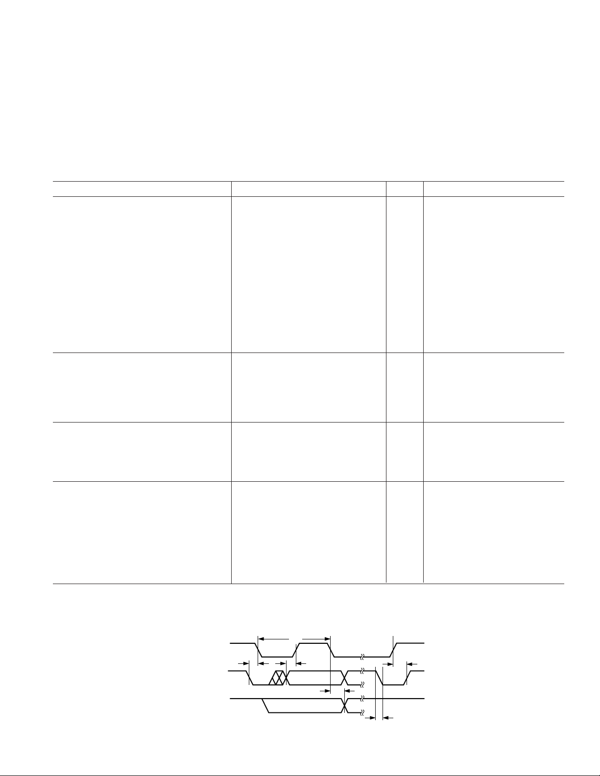
SCL
SDA
DATA IN
SDA
DATA OUT
t
1
t
4
t
2
t
3
t
6
Figure 1. Diagram for Serial Bus Timing
–3–
t
5

AD7416/AD7417/AD7418
AD7417 PIN FUNCTION DESCRIPTION
Pin No. Mnemonic Description
1, 16 NC No Connection. Do not connect anything to this pin.
2 SDA Digital I/O. Serial bus bidirectional data. Push-pull output.
3 SCL Digital Input. Serial bus clock.
4 OTI This is a logic output. The overtemperature indicator (OTI) is set if the result of a conversion on
Channel 0 (temperature sensor) is greater than an 8-bit word in the overtemperature register (OTR).
The signal is reset at the end of a serial read operation. Open-drain output.
5 REF
IN
6GND Ground reference for track-and-hold, comparator and capacitor DAC, and digital circuitry.
7–10 A
IN1
to A
11 A2 Digital Input. The highest programmable bit of the serial bus address.
12 A1 Digital Input. The middle programmable bit of the serial bus address.
13 A0 Digital Input. The lowest programmable bit of the serial bus address.
14 V
DD
15 CONVST Logic Input Signal. Convert start signal. The rising edge of this signal fully powers up the part. The
Reference Input. An external 2.5 V reference can be connected to the AD7417 at this pin. To enable the
on-chip reference, the REFIN pin should be tied to GND. If an external reference is connected to the
AD7417, the internal reference will shut down.
Analog Input Channels. The AD7417 has four analog input channels. The input channels are single-ended
IN4
with respect to GND. The input channels can convert voltage signals in the range 0 V to V
. A chan-
REF
nel is selected by writing to the configuration register of the AD7417. (See Control Byte section.)
Positive Supply Voltage, 2.7 V to 5.5 V.
power-up time for the part is 4 µs. If the CONVST pulse is greater than 4 µs, the falling edge of CONVST
places the track-and-hold mode into hold mode and initiates a conversion. If the pulse is less than 4 µs,
an internal timer ensures that the track-and-hold does not go into hold and conversion is not initiated
until the power-up time has elapsed. The track-and-hold goes into track mode again at the end of conversion. (See Operating Mode section.)
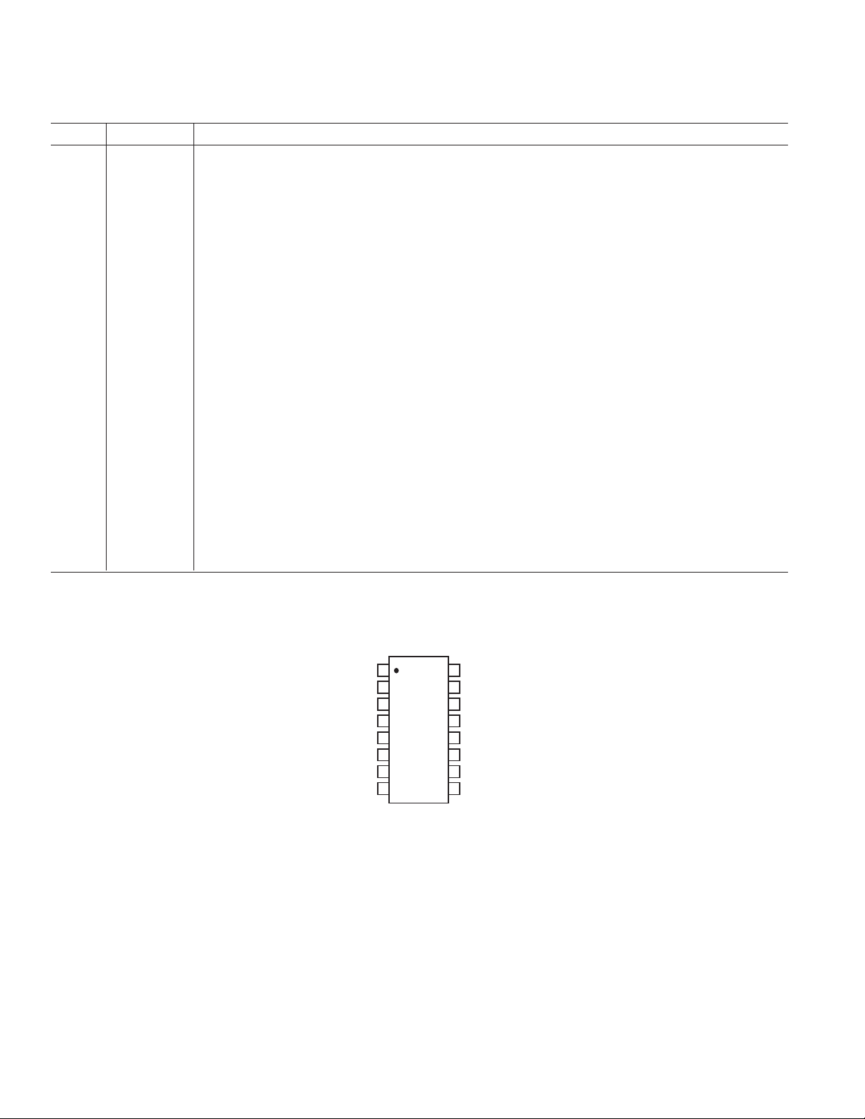
AD7417 PIN CONFIGURATION
SOIC/TSSOP
1
NC
2
SDA
3
SCL
4
OTI
5
REF
IN
6
GND
7
A
IN1
8
A
IN2
NC = NO CONNECT
AD7417
TOP VIEW
(Not to Scale)
16
15
14
13
12
11
10
9
NC
CONVST
V
DD
A0
A1
A2
A
IN4
A
IN3
REV. G–4–

AD7416/AD7417/AD7418
TOP VIEW
(Not to Scale)
8
7
6
5
1
2
3
4
SDA
SCL
OTI
GND
CONVST
V
DD
REF
IN
A
IN
AD7418
AD7416 PIN FUNCTION DESCRIPTION
Pin No. Mnemonic Description
1 SDA Digital I/O. Serial bus bidirectional data. Push-pull output.
2 SCL Digital Input. Serial bus clock.
3 OTI This is a logic output. The OTI is set if the result of a conversion on Channel 0 (temperature sensor) is
greater that an 8-bit word in the OTR. The signal is reset at the end of a serial read operation. Opendrain output.
4GND Ground reference for track-and-hold, comparator and capacitor DAC, and digital circuitry.
5A2Digital Input. The highest programmable bit of the serial bus address.
6A1Digital Input. The middle programmable bit of the serial bus address.
7A0Digital Input. The lowest programmable bit of the serial bus address.
8VDDPositive Supply Voltage, 2.7 V to 5.5 V.
AD7418 PIN FUNCTION DESCRIPTION
Pin No. Mnemonic Description
1 SDA Digital I/O. Serial bus bidirectional data. Push-pull output.
2 SCL Digital Input. Serial bus clock.
3 OTI This is a logic output. The OTI is set if the result of a conversion on Channel 0 (temperature sensor) is
greater that an 8-bit word in the OTR. The signal is reset at the end of a serial read operation. Opendrain output.
4GND Ground reference for track-and-hold, comparator and capacitor DAC, and digital circuitry.
5A
6 REF
7V
IN
IN
DD
8 CONVST Logic Input Signal. Convert start signal. The rising edge of this signal fully powers up the part. The
Analog Input Channel. The input channel is single-ended with respect to GND. The input channel can
convert voltage signals in the range 0 V to V
. The analog input channel is selected by writing to the
REF
configuration register of the AD7418 and choosing Channel 4. (See Control Byte section.)
Reference Input. An external 2.5 V reference can be connected to the AD7418 at this pin. To enable the
on-chip reference, the REF
pin should be tied to GND. If an external reference is connected to the
IN
AD7418, the internal reference will shut down.
Positive Supply Voltage, 2.7 V to 5.5 V.
power-up time for the part is 4 µs. If the CONVST pulse is greater than 4 µs, the falling edge of
CONVST places the track-and-hold mode into hold mode and initiates a conversion. If the pulse is less
than 4 µs, an internal timer ensures that the track-and-hold does not go into hold and conversion is not
initiated until the power-up time has elapsed. The track-and-hold goes into track mode again at the end
of conversion. (See Operating Mode section.)
REV. G
AD7416 PIN CONFIGURATION
SOIC/MSOP
1
SDA
2
OTI
AD7416
TOP VIEW
3
(Not to Scale)
4
SCL
GND
AD7418 PIN CONFIGURATION
SOIC/MSOP
8
V
DD
7
A0
6
A1
5
A2
–5–

AD7416/AD7417/AD7418
ABSOLUTE MAXIMUM RATINGS
1
(TA = 25°C, unless otherwise noted.)
to AGND . . . . . . . . . . . . . . . . . . . . . . . . . –0.3 V to +7 V
V
DD
to DGND . . . . . . . . . . . . . . . . . . . . . . . . . –0.3 V to +7 V
V
DD
Analog Input Voltage to AGND
A
to A
IN1
Reference Input Voltage to AGND
Digital Input Voltage to DGND . . . . . –0.3 V to V
Digital Output Voltage to DGND . . . . –0.3 V to V
. . . . . . . . . . . . . . . . . . . –0.3 V to VDD + 0.3 V
IN4
2
. . –0.3 V to VDD + 0.3 V
DD
DD
+ 0.3 V
+ 0.3 V
Operating Temperature Range
A Version . . . . . . . . . . . . . . . . . . . . . . . . . –40°C to +125°C
B Version . . . . . . . . . . . . . . . . . . . . . . . . . . –40°C to +85°C
Storage Temperature Range . . . . . . . . . . . . –65°C to +150°C
Junction Temperature . . . . . . . . . . . . . . . . . . . . . . . . . . 150°C
TSSOP, Power Dissipation . . . . . . . . . . . . . . . . . . . . 450 mW
Thermal Impedance . . . . . . . . . . . . . . . . . . . . . 120°C/W
JA
Lead Temperature, Soldering . . . . . . . . . . . . . . . . . . 260°C
Vapor Phase (60 sec) . . . . . . . . . . . . . . . . . . . . . . . 215°C
Infrared (15 sec) . . . . . . . . . . . . . . . . . . . . . . . . . . . 220°C
16-Lead SOIC Package, Power Dissipation . . . . . . . . 450 mW
Thermal Impedance . . . . . . . . . . . . . . . . . . . . . 100°C/W
JA
Lead Temperature, Soldering
Vapor Phase (60 sec) . . . . . . . . . . . . . . . . . . . . . . . 215°C
Infrared (15 sec) . . . . . . . . . . . . . . . . . . . . . . . . . . . 220°C
8-Lead SOIC Package, Power Dissipation . . . . . . . . . 450 mW
Thermal Impedance . . . . . . . . . . . . . . . . . . . . . 157°C/W
JA
Lead Temperature, Soldering
Vapor Phase (60 sec) . . . . . . . . . . . . . . . . . . . . . . . 215°C
Infrared (15 sec) . . . . . . . . . . . . . . . . . . . . . . . . . . . 220°C
MSOP Package, Power Dissipation . . . . . . . . . . . . . . 450 mW
Thermal Impedance . . . . . . . . . . . . . . . . . . . . . 206°C/W
JA
Lead Temperature, Soldering
Vapor Phase (60 sec) . . . . . . . . . . . . . . . . . . . . . . . 215°C
Infrared (15 sec) . . . . . . . . . . . . . . . . . . . . . . . . . . . 220°C
NOTES
1
Stresses above those listed under Absolute Maximum Ratings may cause permanent damage to the device. This is a stress rating only; functional operation of the
device at these or any other conditions above those listed in the operational
sections of this specification is not implied. Exposure to absolute maximum rating
conditions for extended periods may affect device reliability.
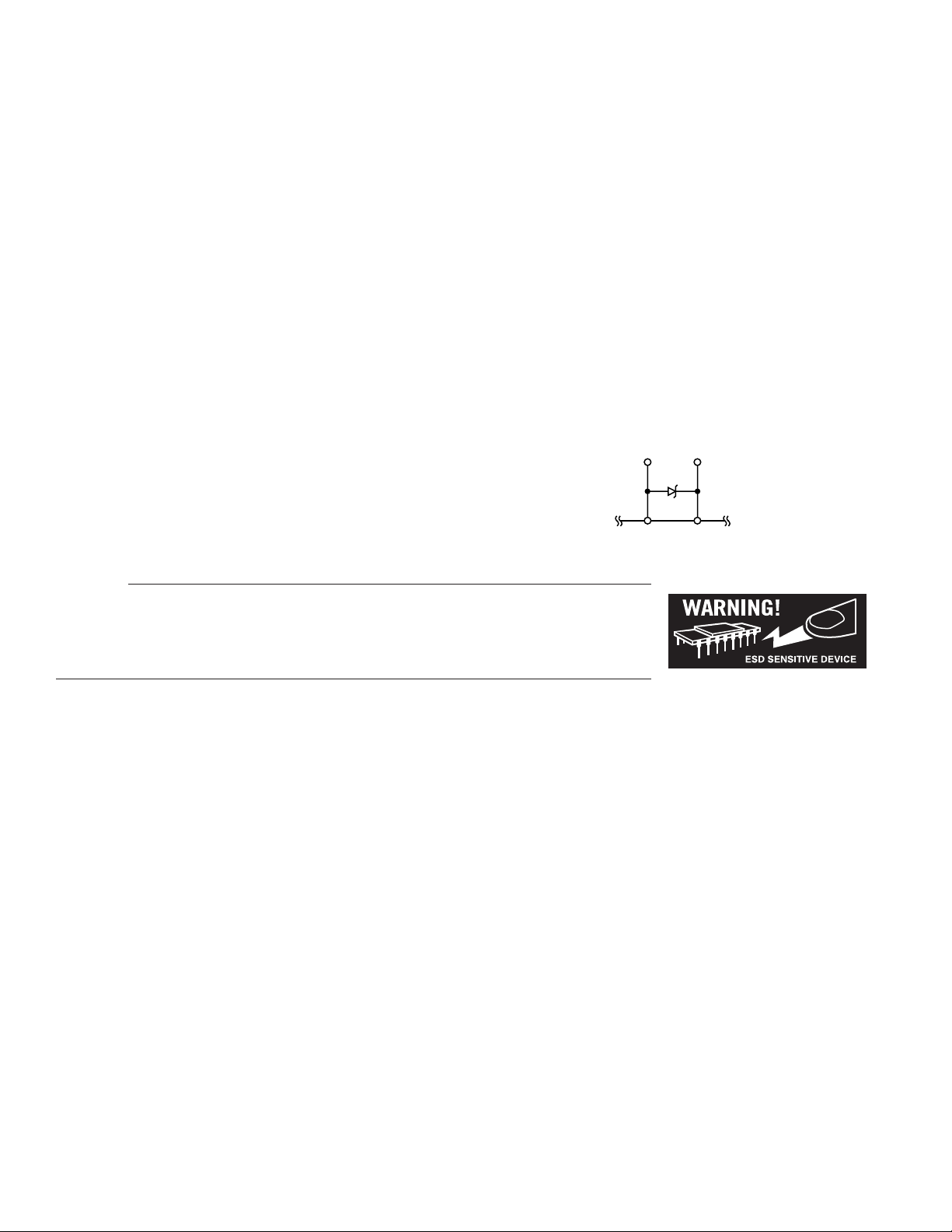
2
If the reference input voltage is likely to exceed VDD by more than 0.3 V (e.g.,
during power-up) and the reference is capable of supplying 30 mA or more, it is
recommended to use a clamping diode between the REFIN pin and VDD pin. The
diagram below shows how the diode should be connected.
REF
IN
BAT81
AD7417
V
DD
CAUTION
ESD (electrostatic discharge) sensitive device. Electrostatic charges as high as 4000 V readily
accumulate on the human body and test equipment and can discharge without detection. Although the
AD7416/AD7417/AD7418 features proprietary ESD protection circuitry, permanent damage may
occur on devices subjected to high energy electrostatic discharges. Therefore, proper ESD precautions
are recommended to avoid performance degradation or loss of functionality.
REV. G–6–
 Loading...