Low Cost, Low Power
Mono Audio Codec
AD74111
FEATURES
2.5 V Mono Audio Codec with 3.3 V Tolerant
Digital Interface
Supports 8 kHz to 48 kHz Sample Rates
Supports 16-/20-/24-Bit Word Lengths
Multibit - Modulators with
“Perfect Differential Linearity Restoration” for
Reduced Idle Tones and Noise Floor
Data Directed Scrambling DAC – Least Sensitive to Jitter
Performance (20 Hz to 20 kHz)
85 dB ADC Dynamic Range
93 dB DAC Dynamic Range
Programmable ADC Gain
On-Chip Volume Control for DAC Channel
Software Controllable Clickless Mute
Supports 256 f
, 512 fS, and 768 fS Master Mode
S
Clocks
Master Clock Prescaler for Use with DSP Master Clocks
On-Chip Reference
16-Lead TSSOP Package
APPLICATIONS
Digital Video Camcorders (DVC)
®
Portable Audio Devices (Walkman
, PDAs, and so on)
Audio Processing
Voice Processing
Telematic Systems
General-Purpose Analog I/O
GENERAL DESCRIPTION
The AD74111 is a front-end processor for general-purpose audio
and voice applications. It features a multibit ⌺-⌬ A/D conversion
channel and a multibit ⌺-⌬ D/A conversion channel. The ADC
channel provides >67 dB THD+N and the DAC channel provides >88 dB THD+N, both over an audio signal bandwidth.
The AD74111 is particularly suitable for a variety of applications
where mono input and output channels are required, including
audio sections of digital video camcorders, portable personal
audio devices, and telematic applications. Its high quality
performance also makes it suitable for speech and telephony
applications such as speech recognition and synthesis, and modern
feature phones.
An on-chip reference voltage is included but can be powered
down and bypassed by an external reference source if required.
The AD74111 offers sampling rates that, depending on MCLK
selection and MCLK divider ratio, range from 8 kHz in the
voiceband range to 48 kHz in the audio range.
The AD74111 is available in a 16-lead TSSOP package option
and is specified for the automotive temperature range of –40°C
to +105°C.
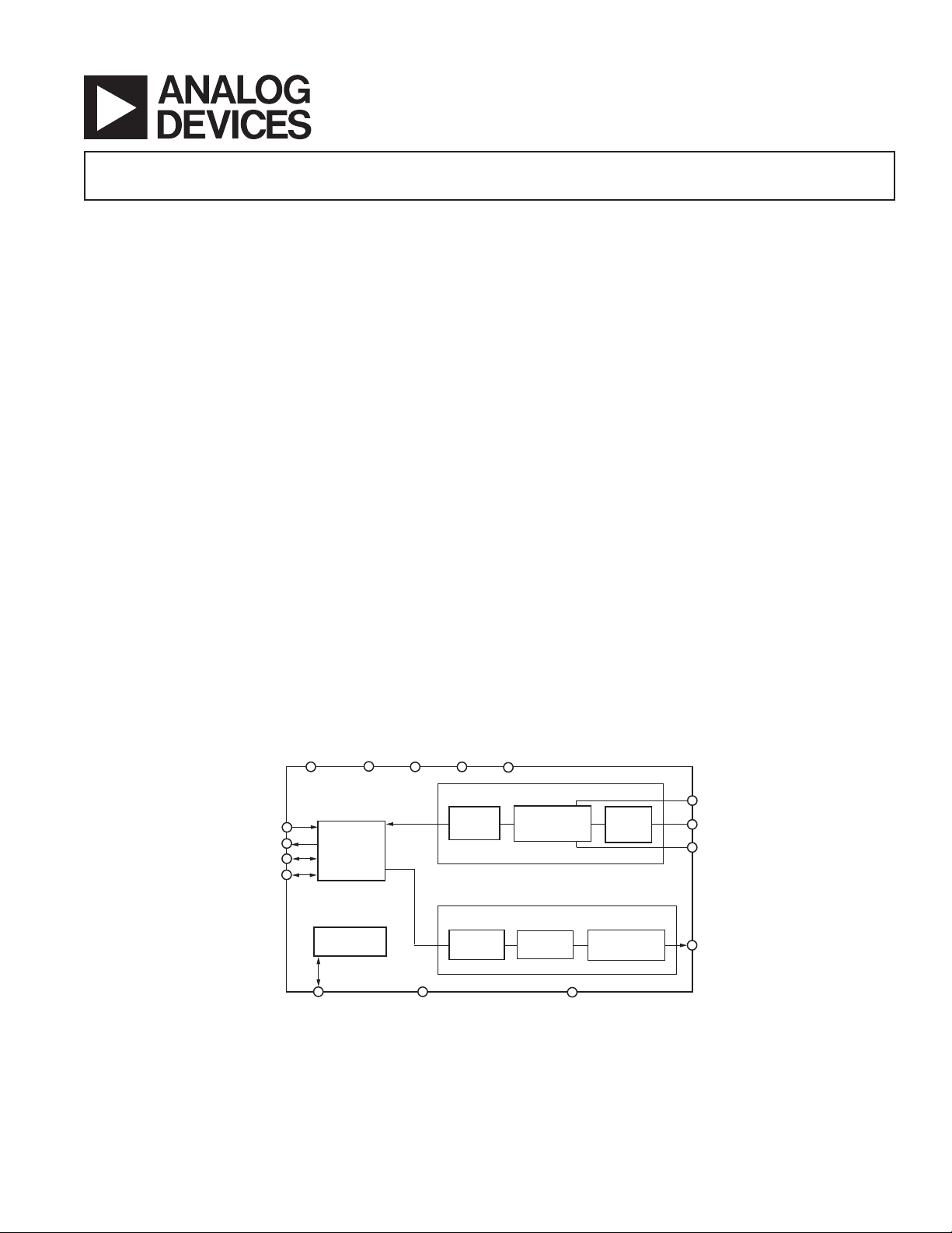
FUNCTIONAL BLOCK DIAGRAM
RESET
DIN
DOUT
DFS
DCLK
REFCAP
MCLK
SERIAL
DATA
PORT
REFERENCE
DGND
DVDD2 AVDDDVDD1
DIGITAL
FILTER
DIGITAL
FILTER
REV. 0
Information furnished by Analog Devices is believed to be accurate and
reliable. However, no responsibility is assumed by Analog Devices for its
use, nor for any infringements of patents or other rights of third parties that
may result from its use. No license is granted by implication or otherwise
under any patent or patent rights of Analog Devices. Trademarks and
registered trademarks are the property of their respective companies.
ADC
AGND
GAIN
STAGE
- DAC
MODULATOR
-
MODULATOR
DAC CHANNEL
VOLUME
CONTROL
One Technology Way, P.O. Box 9106, Norwood, MA 02062-9106, U.S.A.
Tel: 781/329-4700 www.analog.com
Fax: 781/326-8703 © 2003 Analog Devices, Inc. All rights reserved.
CAPP
VIN
CAPN
VOUT

AD74111–SPECIFICATIONS
(AVDD = 2.5 V ± 5%, DVDD2 = 2.5 V ± 5%, DVDD1 = 2.5 V ± 5%, f
fS = 48 kHz, TA = T
MIN
to T
, unless otherwise noted.)
MAX
= 12.288 MHz,
MCLK
Parameter Conditions Min Typ Max Unit
ANALOG-TO-DIGITAL CONVERTERS
ADC Resolution 24 Bits
Signal to Noise Ratio (SNR) f
= 16 kHz 70 77 dB
S
Dynamic Range
(20 Hz to 20 kHz, –60 dB Input)
No Filter fS = 48 kHz 85 dB
f
= 16 kHz 78 85 dB
With A-Weighted Filter f
Total Harmonic Distortion + Noise f
S
= 48 kHz 87 dB
S
= 48 kHz, PGA = 0 dB –67 dB
S
f
= 16 kHz –75 dB
S
Programmable Input Gain 12 dB
Gain Step Size 3dB
Offset Error –55 +30 +80 mV
Full-Scale Input Voltage 0.5 V rms
Input Resistance 4kΩ
Input Capacitance 15 pF
Common-Mode Input Volts 1.125 V
Crosstalk
ADC Input Signal = 1.0 kHz,
100 dB
0 dB; DAC Output = DC
DIGITAL-TO-ANALOG CONVERTERS
DAC Resolution 24 Bits
Signal to Noise Ratio (SNR) f
= 16 kHz 80 89 dB
S
Dynamic Range
(20 Hz to 20 kHz, –60 dB Input)
No Filter f
With A-Weighted Filter f
Total Harmonic Distortion + Noise
= 48 kHz 93 dB
S
= 16 kHz 84 93 dB
f
S
= 48 kHz 95 dB
S
fS = 48 kHz –88 dB
f
= 16 kHz –88 –81 dB
S
dB
DC Accuracy
Offset Error –75 –10 +50 mV
Gain Error –0.9 +0.175 +0.8 dB
Volume Control Step Size
(1024 Linear Steps) 0.098 %
Volume Control Range (Max Attenuation) –60 dB
Mute Attenuation –100 dB
De-emphasis Gain Error ± 0.1 dB
Full-Scale Output Voltage 0.5 V rms
Output Resistance 145 Ω
Common Mode Output Volts 1.125 V
Crosstalk
Signal Input ADC = AGND; 95 dB
DAC Output
Level = 1.0 kHz, 0 dB
REFERENCE (Internal)
Absolute Voltage, V
V
TC 50 ppm/°C
REF
REF
1.125 V
REV. 0–2–

AD74111
Parameter Conditions Min Typ Max Unit
ADC DECIMATION FILTER* f
Pass Band 21.5 kHz
Pass-Band Ripple 0.2 mdB
Transition Band 5 kHz
Stop Band 26.5 kHz
Stop-Band Attenuation 120 dB
Group Delay 910 µs
Low Group Delay Mode 87 µs
DAC INTERPOLATION FILTER* f
Pass Band 21.5 kHz
Pass-Band Ripple 10 mdB
Transition Band 5 kHz
Stop Band 26.5 kHz
Stop-Band Attenuation 75 dB
Group Delay 505 µs
Low Group Delay Mode 55 µs
LOGIC INPUT
, Input High Voltage DVDD1 – 0.8 DVDD1 V
V
INH
V
, Input Low Voltage 0 0.8 V
INL
Input Current –10 +10 µA
Input Capacitance 10 pF
LOGIC OUTPUT
VOH, Output High Voltage DVDD1 – 0.4 DVDD1 V
V
, Output Low Voltage 0 0.4 V
OL
Three-State Leakage Current –10 +10 µA
POWER SUPPLIES
AVDD 2.375 2.625 V
DVDD2 2.375 2.625 V
DVDD1 2.375 3.6 V
Power Supply Rejection Ratio
1 kHz, 300 mV p-p Signal at Analog
Supply Pins 72 dB
50/60 Hz, 300 mV p-p Signal at Analog
Supply Pins 73 dB
*Guaranteed by design.
Specifications subject to change without notice.
= 48 kHz
S
= 48 kHz
S
REV. 0
Table I. Current Summary (AVDD = 2.5 V, DVDD1 = 2.5 V, DVDD2 = 2.5 V)
1, 2, 3
AVDD DVDD1 DVDD2 Total Current
Conditions Current (mA) Current (mA) Current (mA) (Max)(mA)
ADC, Reference, Ref-Amp On 6.11 (6.11) 0.15 (0.43) 0.72 (2.10)
DAC, Reference, Ref-Amp On 3.80 (4.0) 0.15 (0.43) 0.85 (2.23)
Reference, Ref-Amp On 0.60 (0.60) 0.15 (0.43) 0.27 (0.50)
All Sections On 8.60 0.15 (0.43) 1.72 (4.80) 15.35
Power-Down Mode 0.035 0.15 (0.43) 0.49 (0.49) 2.6
NOTES
1
All values are typical, unless otherwise noted.
2
Max values are quoted with DVDD1 = 3.6 V.
3
Sample rates quoted are for 16 kHz and (48 kHz).
–3–

AD74111
(AVDD = 2.5 V ± 5%, DVDD2 = 2.5 V ± 5%, DVDD1 = 3.3 V ± 10%, f
TIMING CHARACTERISTICS
TA = T
MIN
to T
, unless otherwise noted.)
MAX
Parameter Min Max Unit Comments
MASTER CLOCK AND RESET
t
MH
t
ML
t
RES
t
RS
t
RH
SERIAL PORT
t
CH
t
CL
t
FD
t
FS
t
FH
t
DD
t
DS
t
DH
t
DT
NOTES
1
Determines Master/Slave mode operation.
2
Applies in Slave mode only.
3
Applies in Master mode only.
4
Applies in Multiframe-Sync mode only.
MCLK High 25 ns
MCLK Low 25 ns
RESET Low 10 ns
DIN Setup Time 5 MCLKS To RESET Rising Edge
DIN Setup Time 5 MCLKS To RESET Rising Edge
DCLK High
DCLK Low
2
2
20 ns
20 ns
DFS Delay 5 ns From DCLK Rising Edge
DFS Setup Time 5 ns To DCLK Falling Edge
DFS Hold Time 15 ns From DCLK Falling Edge
DOUT Delay 30 ns From DCLK Rising Edge
DIN Setup Time 5 ns To DCLK Falling Edge
DIN Hold Time 15 ns From DCLK Falling Edge
DOUT Three-State 40 ns From DCLK Rising Edge
t
MH
MCLK
= 12.288 MHz, fS = 48 kHz,
MCLK
1
1
3
4
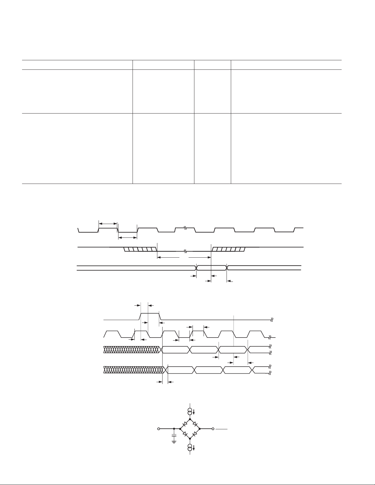
RESET
DIN
DFS
DCLK
DIN
DOUT
t
ML
Figure 1. MCLK and
t
FS
t
FH
t
FD
t
DD
Figure 2. Serial Port Timing
t
RES
t
RS
t
RH
RESET
Timing
t
CH
t
CL
MSB MSB–1
MSB MSB–2
100A
MSB–1
I
OL
MSB–2
t
DS
t
DH
TO OUTPUT
PIN
50pF
C
L
100A
I
OH
DVDD1
2
Figure 3. Load Circuit for Digital Output Timing Specifications
REV. 0–4–

AD74111
ABSOLUTE MAXIMUM RATINGS*
(TA = 25°C, unless otherwise noted.)
AVDD, DVDD2 to AGND, DGND . . . . . . . –0.3 V to +3.0 V
DVDD1 to AGND, DGND . . . . . . . . . . . . . –0.3 V to +4.5 V
AGND to DGND . . . . . . . . . . . . . . . . . . . . . –0.3 V to +0.3 V
Digital I/O Voltage to DGND . . . . . . –0.3 V to DVDD1 + 0.3 V
Operating Temperature Range
Automotive (Y Version) . . . . . . . . . . . . . . –40°C to +105°C
Storage Temperature Range . . . . . . . . . . . . . –65°C to +150°C
Junction Temperature . . . . . . . . . . . . . . . . . . . . . . . . . . 150°C
TEMPERATURE RANGE
Parameter Min Max Unit
Specifications Guaranteed –40 +105 ºC
Storage –65 +150 ºC
16-Lead TSSOP, θ
Thermal Impedance . . . . . . . .150.4°C/W
JA
Lead Temperature, Soldering
Vapor Phase (60 sec) . . . . . . . . . . . . . . . . . . . . . . . . . 215°C
Infrared (15 sec) . . . . . . . . . . . . . . . . . . . . . . . . . . . . 220°C
*Stresses above those listed under Absolute Maximum Ratings may cause perma-
nent damage to the device. This is a stress rating only; functional operation of the
device at these or any other conditions above those listed in the operational
sections of this specification is not implied. Exposure to absolute maximum rating
conditions for extended periods may affect device reliability.
ORDERING GUIDE
Model Range Package
AD74111YRU –40ºC to +105ºC RU-16
CAUTION
ESD (electrostatic discharge) sensitive device. Electrostatic charges as high as 4000 V readily
accumulate on the human body and test equipment and can discharge without detection. Although the
AD74111 features proprietary ESD protection circuitry, permanent damage may occur on devices
subjected to high energy electrostatic discharges. Therefore, proper ESD precautions are recommended
to avoid performance degradation or loss of functionality.
REV. 0
–5–

AD74111
R
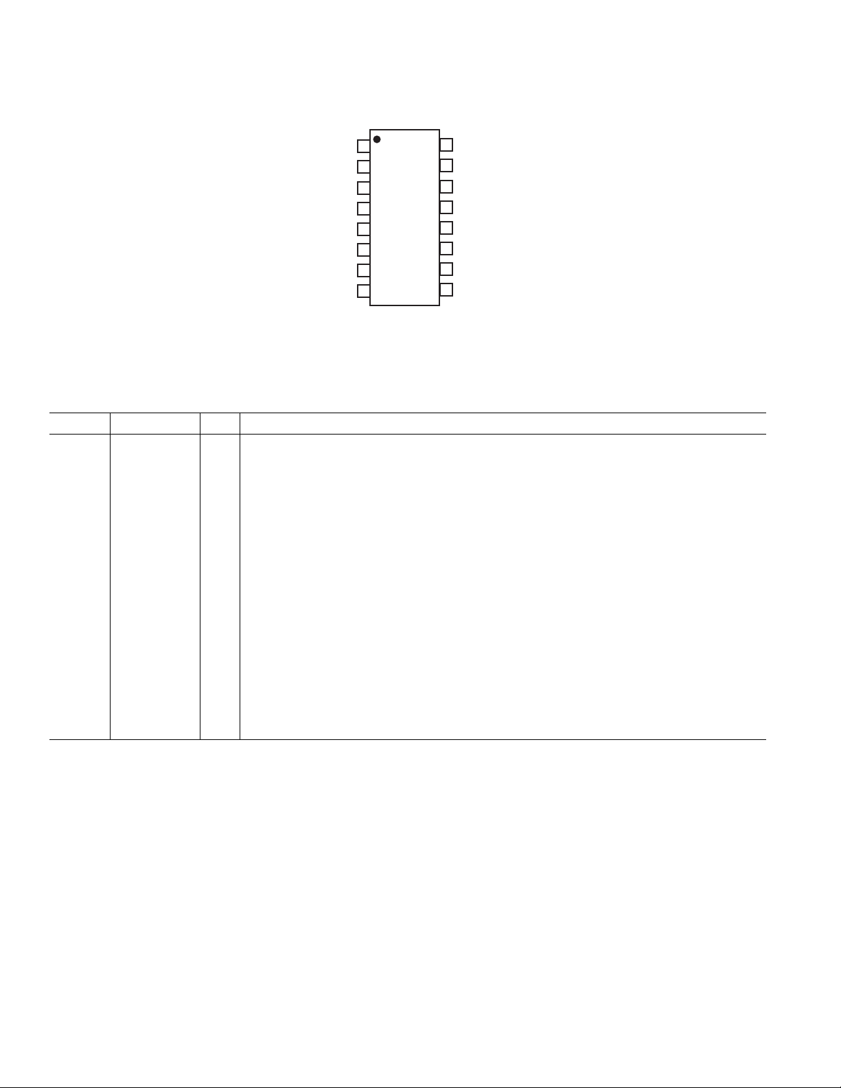
PIN CONFIGURATION
16
15
14
13
12
11
10
9
MCLK
DVDD1
DVDD2
DGND
AGND
REFCAP
CAPP
VIN
DCLK
1
DIN
2
DFS
3
DOUT
ESET
AVDD
CAPN
VOUT
AD74111
4
TOP VIEW
(NOT TO SCALE)
5
6
7
8
PIN FUNCTION DESCRIPTIONS
Pin No. Mnemonic I/O Description
1 DCLK I/O Serial Clock
2DIN I Serial Data Input. The state of DIN on the rising edge of RESET determines the operating mode
of the interface. See the Selecting Master or Slave Mode section for more information.
3 DFS I/O Frame Synchronization Signal
4 DOUT O Serial Data Output
5 RESET IPower-Down/Reset Input
6 AVDD Analog 2.5 V Power Supply Connection
7 CAPN ADC Filter Capacitor (Negative)
8 VOUT O DAC Analog Output
9VIN I ADC Analog Input
10 CAPP ADC Filter Capacitor (Positive)
11 REFCAP I/O Internal Reference Decoupling Capacitor. Can also be used for connection of an external reference.
12 AGND Analog Ground Connection
13 DGND Digital Ground Connection
14 DVDD2 Digital 2.5 V Power Supply Connection (Core)
15 DVDD1 Digital Power Supply Connection (Interface)
16 MCLK I External Master Clock Input
REV. 0–6–
 Loading...