Analog Devices AD7398BRU-REEL, AD7398BR-REEL, AD7398BR, AD7399BRU-REEL7, AD7399BR Datasheet
...
REV. 0
Information furnished by Analog Devices is believed to be accurate and
reliable. However, no responsibility is assumed by Analog Devices for its
use, nor for any infringements of patents or other rights of third parties
which may result from its use. No license is granted by implication or
otherwise under any patent or patent rights of Analog Devices.
a
AD7398/AD7399
One Technology Way, P.O. Box 9106, Norwood, MA 02062-9106, U.S.A.
Tel: 781/329-4700 World Wide Web Site: http://www.analog.com
Fax: 781/326-8703 © Analog Devices, Inc., 2000
Quad, Serial-Input
12-Bit/10-Bit DACs
FUNCTIONAL BLOCK DIAGRAM
CLK
GND
V
DD
CS
SDI
DAC A
REGISTER
DAC A
INPUT
REG A
INPUT
REG B
INPUT
REG C
INPUT
REG D
SERIAL
REGISTER
POWER
ON RESET
DAC B
REGISTER
DAC C
REGISTER
DAC D
REGISTER
DAC D
DAC C
DAC B
V
OUT
A
V
OUT
B
V
OUT
C
V
OUT
D
V
REF
A
V
REF
B
V
REFCVREF
D
LDACRS
V
SS
12/10
FEATURES
AD7398—12-Bit Resolution
AD7399—10-Bit Resolution
Programmable Power Shutdown
Single (3 V to 5 V) or Dual (ⴞ5 V) Supply Operation
3-Wire Serial SPI-Compatible Interface
Internal Power ON Reset
Double Buffered Registers for Simultaneous
Multichannel DAC Update
Four Separate Rail-to-Rail Reference Inputs
Thin Profile TSSOP-16 Package Available
Low Tempco 1.5 ppm/ⴗC
APPLICATIONS
Automotive Output Voltage Span
Portable Communications
Digitally Controlled Calibration
PC Peripherals
GENERAL DESCRIPTION
The AD7398/AD7399 family of quad, 12-bit/10-bit, voltageoutput digital-to-analog converters is designed to operate from a
single 3 V to 5 V or a dual ±5 V supply. Built with Analog’s robust
CBCMOS process, this monolithic DAC offers the user low
cost, and ease-of-use in single or dual-supply systems.
The applied external reference V
REF
determines the full-scale
output voltage. Valid V
REF
values include VSS < V
REF
< V
DD
that
result in a wide selection of full-scale outputs. For multiplying
applications ac inputs can be as large as ±5 V
P
.
A doubled-buffered serial-data interface offers high-speed,
3-wire, SPI and microcontroller-compatible inputs using serialdata-in (SDI), clock (CLK), and a chip-select (CS). A common
level-sensitive load-DAC strobe (LDAC) input allows simultaneous update of all DAC outputs from previously loaded Input
Registers. Additionally, an internal power ON reset forces the
output voltage to zero at system turn ON. An external asynchronous reset (RS) also forces all registers to the zero code state. A
programmable power-shutdown feature reduces power dissipation on unused DACs.
Both parts are offered in the same pinout to enable users to
select the appropriate resolution for their application without
redesigning the layout. For 8-bit resolution applications see the
pin compatible AD7304 product.
The AD7398/AD7399 is specified over the extended industrial
(–40°C to +125°C) temperature range. Parts are available in
wide body SOIC-16 and ultracompact thin 1.1 mm TSSOP16 packages.
CODE – Decimal
–0.50
0
512
DNL – LSB
0
–0.40
–0.30
–0.20
–0.10
0.10
0.20
0.30
0.40
0.50
1024 1536
2048
2560 3072 3584
4096
VDD = +5V
V
SS
= –5V
V
REF
= +2.5V
T
A
= 25ⴗC
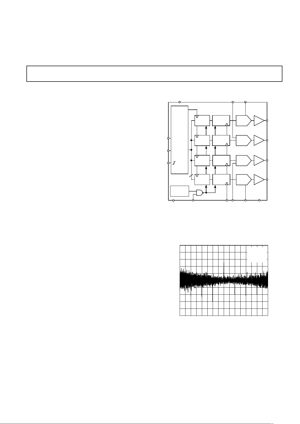
Figure 1. AD7398 DNL vs. Code (TA = 25°C)

REV. 0
–2–
AD7398/AD7399–SPECIFICATIONS
AD7398 12-BIT VOLTAGE OUTPUT DAC
P
arameter Symbol Condition 3 V–5 V ⴞ 10% ⴞ5 V ⴞ 10% Unit
STATIC PERFORMANCE
Resolution
1
N 12 12 Bits
Relative Accuracy
2
INL ±1.5 ±1.5 LSB max
Differential Nonlinearity
2
DNL Monotonic ±1 ±1 LSB max
Zero-Scale Error V
ZSE
Data = 000
H
7 ±2.5 mV max
Full-Scale Voltage Error V
FSE
Data = FFF
H
±2.5 ±2.5 mV max
Full-Scale Tempco
3
TCV
FS
1.5 1.5 ppm/°C typ
REFERENCE INPUT
V
REF
IN Range
4
V
REF
0/V
DD
VSS/V
DD
V min/max
Input Resistance
5
R
REF
Data = 555H, Worst-Case 35 35 kΩ typ
6
Input Capacitance
3
C
REF
5 5 pF typ
ANALOG OUTPUT
Output Current I
OUT
Data = 800H, ∆V
OUT
= 4 LSB ±5 ± 5 mA typ
Capacitive Load
3
C
L
No Oscillation 200 400 pF max
LOGIC INPUTS
Logic Input Low Voltage V
IL
VDD = 3 V 0.5 V max
V
DD
= 5 V 0.8 0.8 V max
Logic Input High Voltage V
IH
CLK Only 80% V
DD
4.0 V min
2.1–2.4 2.4 V min
Input Leakage Current I
IL
11µA max
Input Capacitance
3
C
IL
10 10 pF max
INTERFACE TIMING
3, 7
Clock Frequency f
CLK
11 16.6 MHz max
Clock Width High t
CH
45 30 ns min
Clock Width Low t
CL
45 30 ns min
CS to Clock Set Up t
CSS
10 5 ns min
Clock to CS Hold t
CSH
20 15 ns min
Load DAC Pulsewidth t
LDAC
45 30 ns min
Data Setup t
DS
15 10 ns min
Data Hold t
DH
10 5 ns min
Load Setup to CS t
LDS
0 0 ns min
Load Hold to CS t
LDH
20 15 ns min
AC CHARACTERISTICS
Output Slew Rate SR Data = 000H to FFFH to 000
H
22V/µs typ
Settling Time
8
t
S
To ±0.1% of Full Scale 6 6 µs typ
Shutdown Recovery t
SDR
66µs typ
DAC Glitch Q Code 7FF
H
to 800H to 7FF
H
150 150 nVs typ
Digital Feedthrough Q
DF
15 15 nVs typ
Feedthrough V
OUT/VREFVREF
= 1.5 VDC + 1 V p-p, –63 –63 dB typ
Data = 000H, f = 100 kHz
SUPPLY CHARACTERISTICS
Shutdown Supply Current I
DD_SD
No Load 30/60 30/60 µA typ/max
Positive Supply Current I
DD
VIL = 0 V, No Load 1.5/2.5 1.6/2.7 mA typ/max
Negative Supply Current I
SS
VIL = 0 V, No Load 1.5/2.5 1.6/2.7 mA typ/max
Power Dissipation P
DISS
VIL = 0 V, No Load 5 16 mW typ
Power Supply Sensitivity PSS ∆VDD = ±5% 0.006 0.006 %/% max
NOTES
1
One LSB = V
REF
/4096 V for the 12-bit AD7398.
2
The first eight codes (000H, 007H) are excluded from the linearity error measurement in single supply operation.
3
These parameters are guaranteed by design and not subject to production testing.
4
When V
REF
is connected to either the VDD or the VSS power supply the corresponding V
OUT
voltage will program between ground and the supply voltage minus the
offset voltage of the output buffer, which is the same as the V
ZSE
error specification. See additional discussion in the Operation section of the data sheet.
5
Input resistance is code-dependent.
6
Typicals represent average readings measured at 25°C.
7
All input control signals are specified with tR = tF = 2 ns (10% to 90% of 3 V) and timed from a voltage level of 1.5 V.
8
The settling time specification does not apply for negative going transitions within the last 3 LSBs of ground.
Specifications subject to change without notice.
(@ VDD = 5 V, VSS = 0 V; or VDD = +5 V, VSS = –5 V, V
REF
= +2.5 V, –40ⴗC < T
A
< +125ⴗC, unless otherwise noted.)

REV. 0
–3–
AD7398/AD7399
AD7399 10-BIT VOLTAGE OUTPUT DAC
P
arameter Symbol Condition 3 V–5 V ⴞ 10% ⴞ5 V ⴞ 10% Unit
STATIC PERFORMANCE
Resolution
1
N 10 10 Bits
Relative Accuracy
2
INL ±1 ± 1 LSB max
Differential Nonlinearity
2
DNL Monotonic ±1 ±1 LSB max
Zero-Scale Error V
ZSE
Data = 000
H
7 ±4 mV max
Full-Scale Voltage Error V
FSE
Data = 3FF
H
±15 ± 15 mV max
Full-Scale Tempco
3
TCV
FS
1.5 1.5 ppm/°C typ
REFERENCE INPUT
V
REF
IN Range
4
V
REF
0/V
DD
VSS/V
DD
V min/max
Input Resistance
5
R
REF
Data = 155H, Worst-Case 40 40 kΩ typ
6
Input Capacitance
3
C
REF
5 5 pF typ
ANALOG OUTPUT
Output Current I
OUT
Data = 200H, ∆V
OUT
= 1 LSB ±5 mA typ
Capacitive Load
3
C
L
No Oscillation 200 400 pF max
LOGIC INPUTS
Logic Input Low Voltage V
IL
VDD = 3 V 0.5 V max
V
DD
= 5 V 0.8 0.8 V max
Logic Input High Voltage V
IH
CLK Only 80% V
DD
4.0 V min
2.1–2.4 2.4 V min
Input Leakage Current I
IL
11µA max
Input Capacitance
3
C
IL
10 10 pF max
INTERFACE TIMING
3, 7
Clock Frequency f
CLK
11 16.6 MHz max
Clock Width High t
CH
45 30 ns min
Clock Width Low t
CL
45 30 ns min
CS to Clock Set Up t
CSS
10 5 ns min
Clock to CS Hold t
CSH
20 15 ns min
Load DAC Pulsewidth t
LDAC
45 30 ns min
Data Setup t
DS
15 10 ns min
Data Hold t
DH
10 5 ns min
Load Setup to CS t
LDS
0 0 ns min
Load Hold to CS t
LDH
20 15 ns min
AC CHARACTERISTICS
Output Slew Rate SR Data = 000H to 3FFH to 000
H
22V/µs typ
Settling Time
8
t
S
To ±0.1% of Full Scale 6 6 µs typ
Shutdown Recovery t
SDR
66µs typ
DAC Glitch Q Code 1FF
H
to 200H to 1FF
H
150 150 nVs typ
Digital Feedthrough Q
DF
15 15 nVs typ
Feedthrough V
OUT/VREFVREF
= 1.5 VDC + 1 V p-p, –63 –63 dB typ
Data = 000H, f = 100 kHz
SUPPLY CHARACTERISTICS
Shutdown Supply Current I
DD_SD
No Load 30/60 30/60 µA typ/max
Positive Supply Current I
DD
VIL = 0 V, No Load 1.5/2.5 1.6/2.7 mA typ/max
Negative Supply Current I
SS
VIL = 0 V, No Load 1.5/2.5 1.6/2.7 mA typ/max
Power Dissipation P
DISS
VIL = 0 V, No Load 5 16 mW typ
Power Supply Sensitivity PSS ∆VDD = ±5% 0.006 0.006 %/% max
NOTES
1
One LSB = V
REF
/1024 V for the 10-bit AD7399.
2
The first two codes (000H, 001H) are excluded from the linearity error measurement in single supply operation.
3
These parameters are guaranteed by design and not subject to production testing.
4
When V
REF
is connected to either the VDD or the VSS power supply the corresponding V
OUT
voltage will program between ground and the supply voltage minus the
offset voltage of the output buffer, which is the same as the V
ZSE
error specification. See additional discussion in the Operation section of the data sheet.
5
Input resistance is code-dependent.
6
Typicals represent average readings measured at 25°C.
7
All input control signals are specified with tR = tF = 2 ns (10% to 90% of 3 V) and timed from a voltage level of 1.5 V.
8
The settling time specification does not apply for negative going transitions within the last 3 LSBs of ground.
Specifications subject to change without notice.
(@ VDD = 5 V, VSS = 0 V; or VDD = +5 V, VSS = –5 V, V
REF
= +2.5 V, –40ⴗC < T
A
< +125ⴗC, unless otherwise noted.)

REV. 0
AD7398/AD7399
–4–
ABSOLUTE MAXIMUM RATINGS*
VDD to GND . . . . . . . . . . . . . . . . . . . . . . . . . . . –0.3 V, +7 V
V
SS
to GND . . . . . . . . . . . . . . . . . . . . . . . . . . . . +0.3 V, –7 V
V
REF
to GND . . . . . . . . . . . . . . . . . . . . . . . . . . . . . . VSS, V
DD
Logic Inputs to GND . . . . . . . . . . . . . . . . . . . . –0.3 V, +8 V
V
OUT
to GND . . . . . . . . . . . . . . . . . V
SS
– 0.3 V, VDD + 0.3 V
I
OUT
Short Circuit to GND . . . . . . . . . . . . . . . . . . . . . 50 mA
Thermal Resistance θ
JA
16-Lead SOIC Package (R-16) . . . . . . . . . . . . . . 158°C/W
16-Lead Thin Shrink Surface Mount (RU-16) . . . 180°C/W
Maximum Junction Temperature (T
J
Max) . . . . . . . . 150°C
Package Power Dissipation . . . . . . . . . . . . . (T
J
Max–TA)/θ
JA
ORDERING GUIDE
Resolution Temperature Package Package Container
Model (Bits) Range Description Option Quantity
AD7398BR 12 –40°C to +125°C SOL-16 R-16 48
AD7398BR-REEL7 12 –40°C to +125°C SOL-16 R-16 1,000
AD7398BRU-REEL7 12 –40°C to +125°C TSSOP-16 RU-16 1,000
AD7399BR 10 –40°C to +125°C SOL-16 R-16 48
AD7399BR-REEL7 10 –40°C to +125°C SOL-16 R-16 1,000
AD7399BRU-REEL7 10 –40°C to +125°C TSSOP-16 RU-16 1,000
The AD7398 contains 3254 transistors. The die size measures 108 mil × 144 millimeters.
SDI
CLK
CS
LDAC
t
LDS
t
CSS
t
DS
t
DH
t
CH
t
CL
t
CSH
t
LDH
t
LDAC
SA
SD A1
D11A0 D10
D9 D8 D7 D6 D5 D4 D3 D2
D1 D0
IN
REG
LD
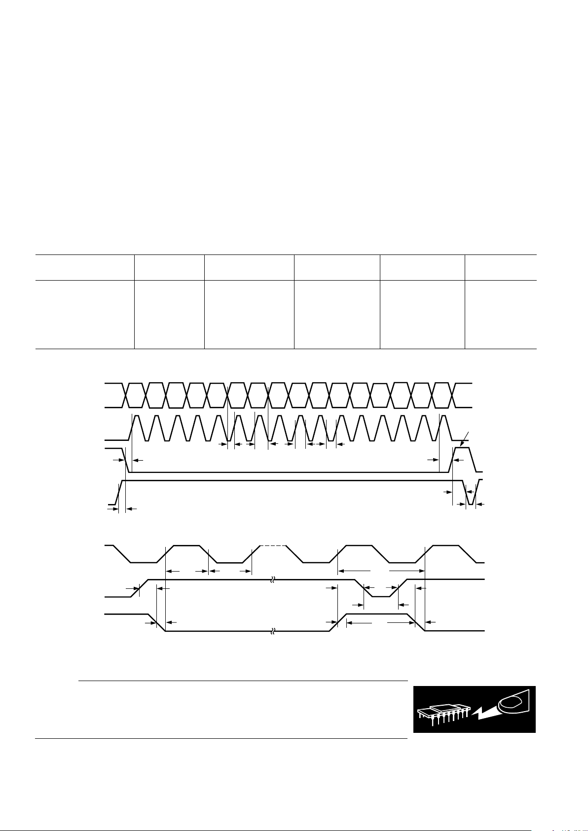
Figure 2. AD7398 Timing Diagram (AD7399 with SDI = 14 Bits Only)
CLK
CS
LDAC
t
LDS
t
CSS
t
LDS
t
CSS
t
CH
t
CL
t
CSH
t
LDH
t
LDAC
1/f
CLK
Figure 3. Continuous Clock Timing Diagram
Operating Temperature Range . . . . . . . . . . –40°C to +125°C
Storage Temperature Range . . . . . . . . . . . . –65°C to +150°C
Lead Temperature
R-16 (Vapor Phase, 60 secs) . . . . . . . . . . . . . . . . . . 215°C
RU-16 (Infrared, 15 secs) . . . . . . . . . . . . . . . . . . . . 224°C
*Stresses above those listed under Absolute Maximum Ratings may cause perma-
nent damage to the device. This is a stress rating only; functional operation of the
device at these or any other conditions above those indicated in the operational
sections of this specification is not implied. Exposure to absolute maximum rating
conditions for extended periods may affect device reliability.
CAUTION
ESD (electrostatic discharge) sensitive device. Electrostatic charges as high as 4000 V readily
accumulate on the human body and test equipment and can discharge without detection. Although
the AD7398/AD7399 features proprietary ESD protection circuitry, permanent damage may occur
on devices subjected to high-energy electrostatic discharges. Therefore, proper ESD precautions
are recommended to avoid performance degradation or loss of functionality.
WARNING!
ESD SENSITIVE DEVICE

REV. 0
AD7398/AD7399
–5–
PIN CONFIGURATION
TOP VIEW
(Not to Scale)
AD7398/
AD7399
CLK
GND
V
DD
CS
SDI
V
OUT
A
V
OUT
BV
OUT
C
V
OUT
D
V
REF
A
V
REF
B
V
REF
C
V
REF
D
LDAC
RS
V
SS
16
15
14
13
12
11
10
98
7
6
5
4
3
2
1
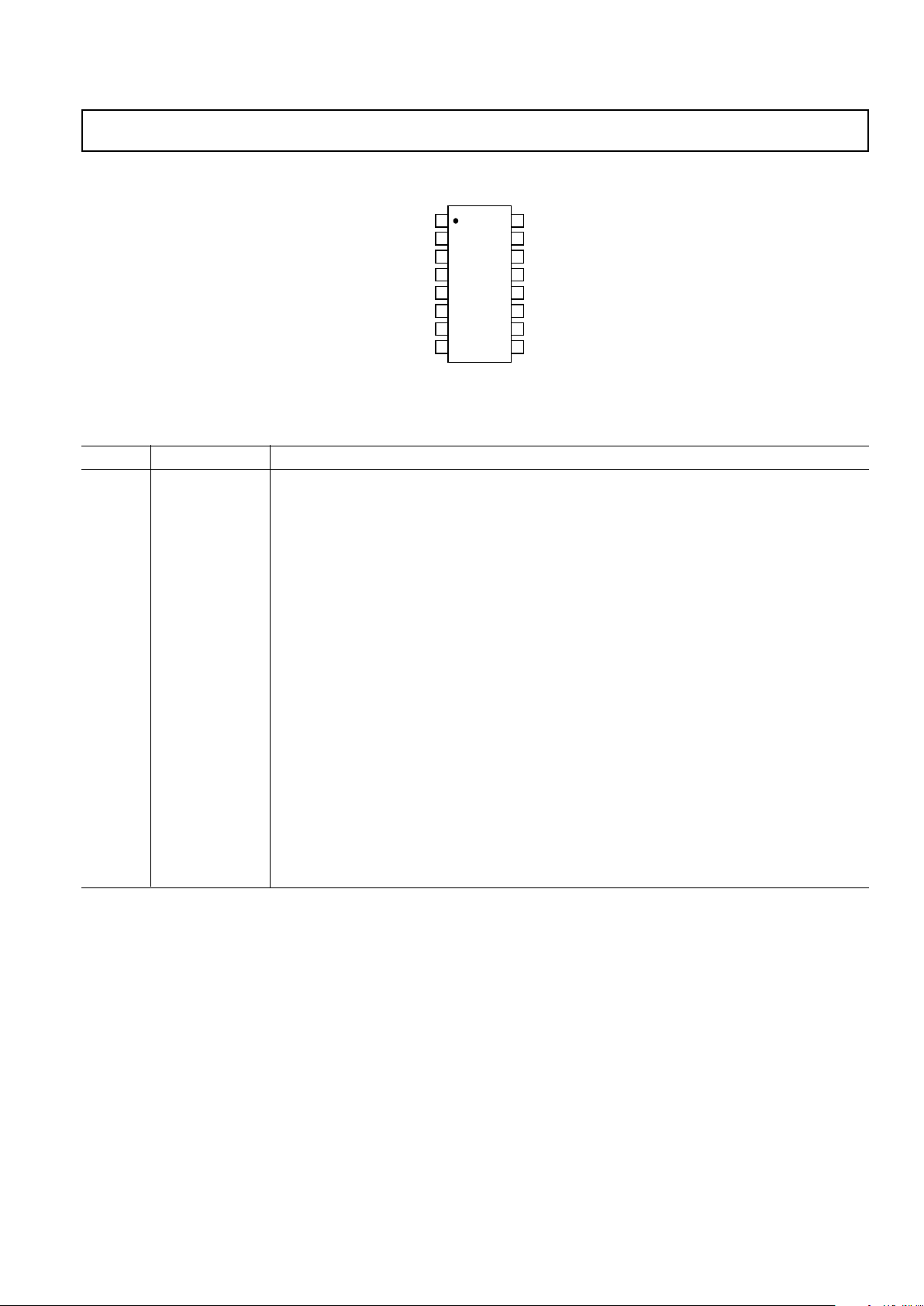
PIN FUNCTION DESCRIPTIONS
Pin No. Mnemonic Function
1V
OUT
B DAC B Voltage Output.
2V
OUT
A DAC A Voltage Output.
3V
SS
Negative Power Supply Input. Specified range of operation 0 V to –5.5 V.
4V
REF
A DAC A Reference Voltage Input Terminal. Establishes DAC A full-scale output voltage. Pin can
be tied to V
DD
or VSS pin.
5V
REF
B DAC B Reference Voltage Input Terminal. Establishes DAC B full-scale output voltage. Pin can
be tied to V
DD
or VSS pin.
6 GND Ground Pin.
7 LDAC Load DAC Register Strobe, Level Sensitive Active Low. Transfers all Input Register data to
DAC registers. Asynchronous active low input. See Control Logic Truth Table for operation.
8 RS Resets Input and DAC Registers to All Zero Codes. Shift Register contents unchanged.
9 CS Chip Select, Active Low Input. Disables shift register loading when high. Transfers Serial Regis-
ter Data to the Input Register when CS returns High. Does not effect LDAC operation.
10 CLK Schmitt Triggered Clock Input, Positive Edge Clocks Data into Shift Register.
11 SDI Serial Data Input. Input data loads directly into the shift register.
12 V
REF
D DAC D Reference Voltage Input Terminal. Establishes DAC D full-scale output voltage. Pin can
be tied to V
DD
or VSS pin.
13 V
REF
C DAC C Reference Voltage Input Terminal. Establishes DAC C full-scale output voltage. Pin can
be tied to V
DD
or VSS pin.
14 V
DD
Positive Power Supply Input. Specified range of operation 3 V to 5 V ± 10%.
15 V
OUT
D DAC D Voltage Output.
16 V
OUT
C DAC C Voltage Output.
 Loading...