Quad, Serial-Input
DAC A
DAC A
REGISTER
INPUT
REG A
DAC B
REGISTER
INPUT
REG B
DAC C
REGISTER
INPUT
REG C
DAC D
REGISTER
INPUT
REG D
SERIAL
REGISTER
POWER
ON RESET
DAC D
DAC C
DAC B
12/10
CLK
V
OUT
A
V
OUT
B
V
OUT
C
V
OUT
D
SDI
V
SS
RS LDAC V
REF
C V
REF
D
GND
CS
V
DD
V
REF
B
V
REF
A
AD7398/AD7399
02179-001
0.5
–0.5
–0.4
–0.3
–0.2
–0.1
0
0.
1
0.2
0.3
0.4
0 4096358430722560204815361024512
DNL (LSB)
CODE (Decimal )
02179-002
VDD = +5V
V
SS
= –5V
V
REF
= +2.5V
T
A
= 25°C
FEATURES
AD7398—12-bit resolution
AD7399—10-bit resolution
Programmable power shutdown
Single (3 V to 5 V) or dual (±5 V) supply operation
3-wire, serial SPI®-compatible interface
Internal power-on reset
Double buffered registers for simultaneous
multichannel DAC update
Four separate rail-to-rail reference inputs
Thin profile, TSSOP-16 package available
Low tempco: 1.5 ppm/°C
Qualified for automotive applications
APPLICATIONS
Automotive output voltage span
Portable communications
Digitally controlled calibration
PC peripherals
GENERAL DESCRIPTION
12-Bit/10-Bit DACs
AD7398/AD7399
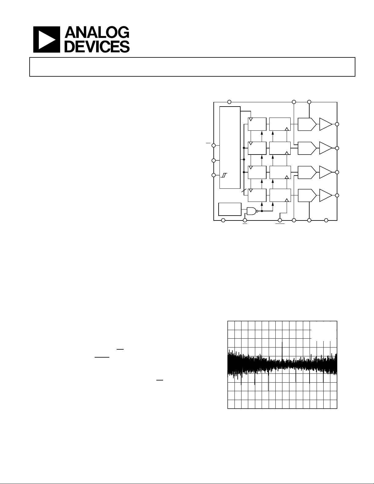
FUNCTIONAL BLOCK DIAGRAM
Figure 1.
The AD7398/AD7399 family of quad, 12-bit/10-bit, voltage
output digital-to-analog converters (DACs) is designed to
operate from a single 3 V to 5 V supply or a dual ±5 V supply.
Built with the Analog Devices, Inc. robust CBCMOS process,
these monolithic DACs offer the user low cost with ease-of-use
in single or dual-supply systems.
Both parts are offered in the same pinout, enabling users to
select the appropriate resolution for their application without
redesigning the layout. For 8-bit resolution applications, see the
pin-compatible AD7304 product.
The AD7398/AD7399 are specified over the extended industrial
(−40°C to +125°C) temperature range. Parts are available in
The applied external reference, V
output voltage. Valid V
values include VSS < V
REF
, determines the full-scale
REF
< VDD that
REF
16-lead, wide body SOIC and ultracompact, thin, 1.1 mm
TSSOP packages.
result in a wide selection of full-scale outputs. For multiplying
applications, ac inputs can be as large as ±5 V
.
P
A doubled-buffered serial-data interface offers high speed, 3-wire,
SPI- and microcontroller-compatible inputs using serial data-in
(SDI), clock (CLK), and a chip-select (
sensitive, load-DAC strobe (
CS
). A common level-
LDAC
) input allows simultaneous
update of all DAC outputs from previously loaded input registers.
Additionally, an internal power-on reset forces the output voltage to
zero at system turn on. An external asynchronous reset (
forces all registers to the zero code state. A programmable powershutdown feature reduces power dissipation on unused DACs.
Rev. C
Information furnished by Analog Devices is believed to be accurate and reliable. However, no
responsibility is assumed by Analog Devices for its use, nor for any infringements of patents or other
rights of third parties that may result from its use. Specifications subject to change without notice. No
license is granted by implication or otherwise under any patent or patent rights of Analog Devices.
Trademarks and registered trademarks are the prop erty of their respective owner s.
RS
) also
One Technology Way, P.O. Box 9106, Norwood, MA 02062-9106, U.S.A.
Tel: 781.329.4700 www.analog.com
Fax: 781.461.3113 ©2000–2011 Analog Devices, Inc. All rights reserved.
Figure 2. AD7398 DNL vs. Code (T
= 25°C)
A
 Loading...