

Analog Devices AD7398BRU-REEL, AD7398BR-REEL, AD7398BR, AD7399BRU-REEL7, AD7399BR Datasheet
...
REV. 0
Information furnished by Analog Devices is believed to be accurate and
reliable. However, no responsibility is assumed by Analog Devices for its
use, nor for any infringements of patents or other rights of third parties
which may result from its use. No license is granted by implication or
otherwise under any patent or patent rights of Analog Devices.
a
AD7398/AD7399
One Technology Way, P.O. Box 9106, Norwood, MA 02062-9106, U.S.A.
Tel: 781/329-4700 World Wide Web Site: http://www.analog.com
Fax: 781/326-8703 © Analog Devices, Inc., 2000
Quad, Serial-Input
12-Bit/10-Bit DACs
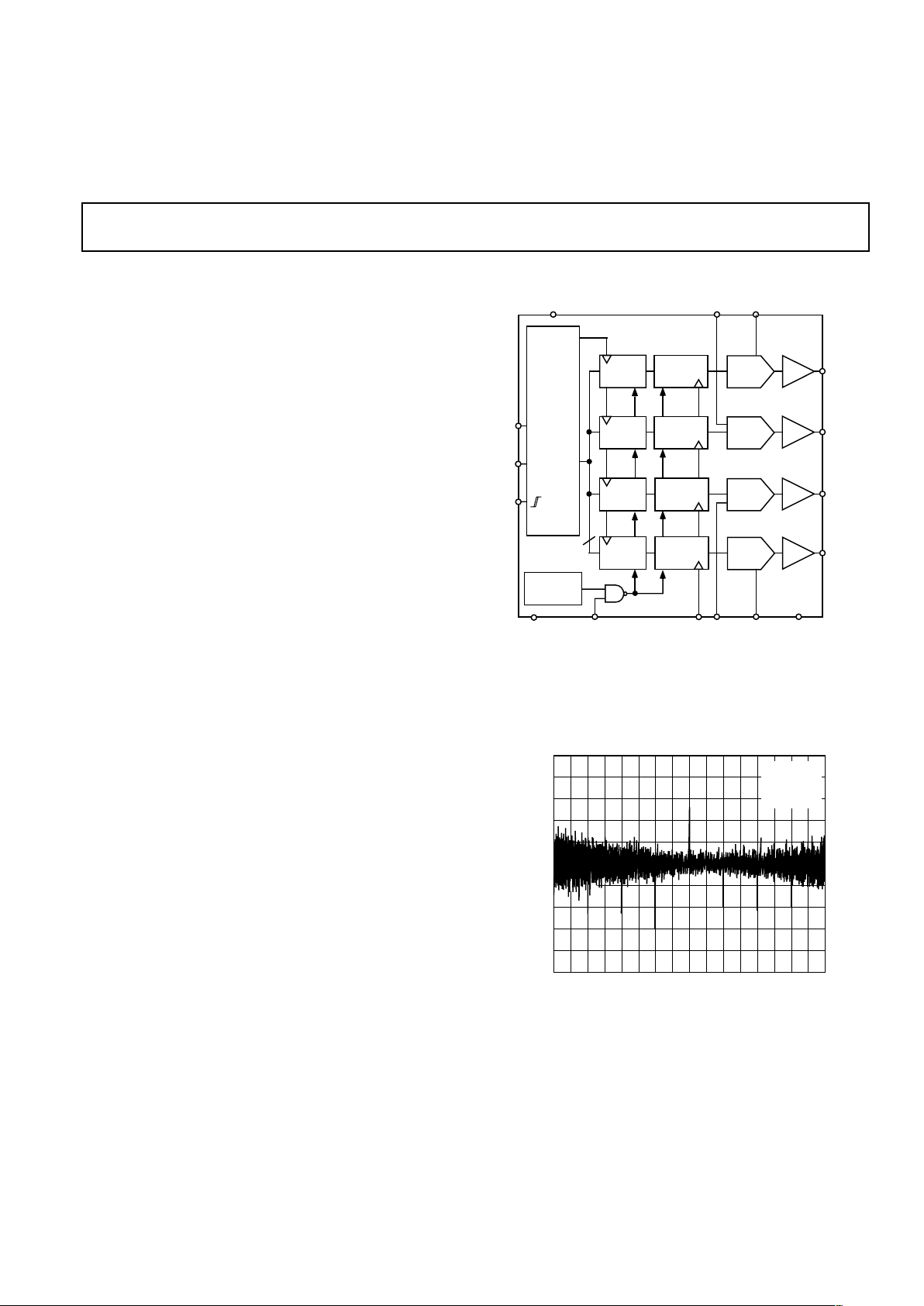
FUNCTIONAL BLOCK DIAGRAM
CLK
GND
V
DD
CS
SDI
DAC A
REGISTER
DAC A
INPUT
REG A
INPUT
REG B
INPUT
REG C
INPUT
REG D
SERIAL
REGISTER
POWER
ON RESET
DAC B
REGISTER
DAC C
REGISTER
DAC D
REGISTER
DAC D
DAC C
DAC B
V
OUT
A
V
OUT
B
V
OUT
C
V
OUT
D
V
REF
A
V
REF
B
V
REFCVREF
D
LDACRS
V
SS
12/10
FEATURES
AD7398—12-Bit Resolution
AD7399—10-Bit Resolution
Programmable Power Shutdown
Single (3 V to 5 V) or Dual (ⴞ5 V) Supply Operation
3-Wire Serial SPI-Compatible Interface
Internal Power ON Reset
Double Buffered Registers for Simultaneous
Multichannel DAC Update
Four Separate Rail-to-Rail Reference Inputs
Thin Profile TSSOP-16 Package Available
Low Tempco 1.5 ppm/ⴗC
APPLICATIONS
Automotive Output Voltage Span
Portable Communications
Digitally Controlled Calibration
PC Peripherals
GENERAL DESCRIPTION
The AD7398/AD7399 family of quad, 12-bit/10-bit, voltageoutput digital-to-analog converters is designed to operate from a
single 3 V to 5 V or a dual ±5 V supply. Built with Analog’s robust
CBCMOS process, this monolithic DAC offers the user low
cost, and ease-of-use in single or dual-supply systems.
The applied external reference V
REF
determines the full-scale
output voltage. Valid V
REF
values include VSS < V
REF
< V
DD
that
result in a wide selection of full-scale outputs. For multiplying
applications ac inputs can be as large as ±5 V
P
.
A doubled-buffered serial-data interface offers high-speed,
3-wire, SPI and microcontroller-compatible inputs using serialdata-in (SDI), clock (CLK), and a chip-select (CS). A common
level-sensitive load-DAC strobe (LDAC) input allows simultaneous update of all DAC outputs from previously loaded Input
Registers. Additionally, an internal power ON reset forces the
output voltage to zero at system turn ON. An external asynchronous reset (RS) also forces all registers to the zero code state. A
programmable power-shutdown feature reduces power dissipation on unused DACs.
Both parts are offered in the same pinout to enable users to
select the appropriate resolution for their application without
redesigning the layout. For 8-bit resolution applications see the
pin compatible AD7304 product.
The AD7398/AD7399 is specified over the extended industrial
(–40°C to +125°C) temperature range. Parts are available in
wide body SOIC-16 and ultracompact thin 1.1 mm TSSOP16 packages.
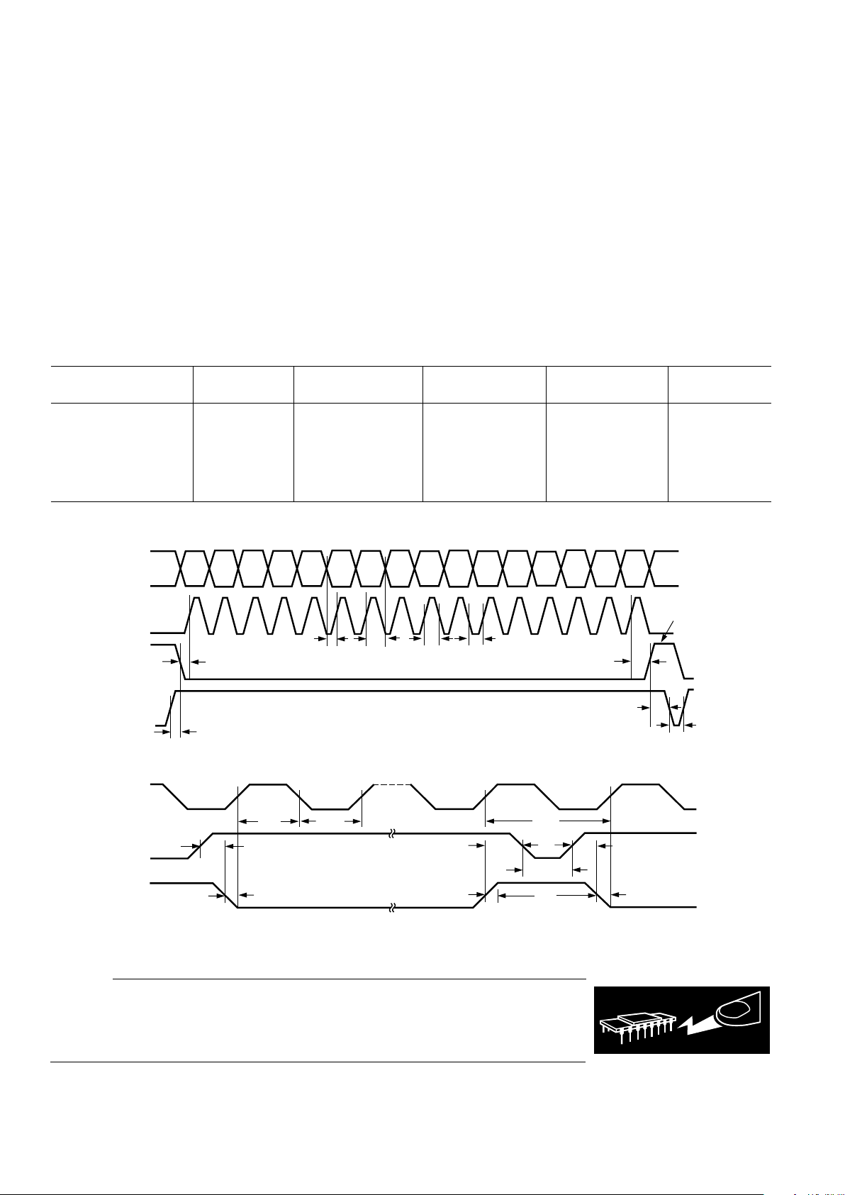
CODE – Decimal
–0.50
0
512
DNL – LSB
0
–0.40
–0.30
–0.20
–0.10
0.10
0.20
0.30
0.40
0.50
1024 1536
2048
2560 3072 3584
4096
VDD = +5V
V
SS
= –5V
V
REF
= +2.5V
T
A
= 25ⴗC
Figure 1. AD7398 DNL vs. Code (TA = 25°C)

REV. 0
–2–
AD7398/AD7399–SPECIFICATIONS
AD7398 12-BIT VOLTAGE OUTPUT DAC
P
arameter Symbol Condition 3 V–5 V ⴞ 10% ⴞ5 V ⴞ 10% Unit
STATIC PERFORMANCE
Resolution
1
N 12 12 Bits
Relative Accuracy
2
INL ±1.5 ±1.5 LSB max
Differential Nonlinearity
2
DNL Monotonic ±1 ±1 LSB max
Zero-Scale Error V
ZSE
Data = 000
H
7 ±2.5 mV max
Full-Scale Voltage Error V
FSE
Data = FFF
H
±2.5 ±2.5 mV max
Full-Scale Tempco
3
TCV
FS
1.5 1.5 ppm/°C typ
REFERENCE INPUT
V
REF
IN Range
4
V
REF
0/V
DD
VSS/V
DD
V min/max
Input Resistance
5
R
REF
Data = 555H, Worst-Case 35 35 kΩ typ
6
Input Capacitance
3
C
REF
5 5 pF typ
ANALOG OUTPUT
Output Current I
OUT
Data = 800H, ∆V
OUT
= 4 LSB ±5 ± 5 mA typ
Capacitive Load
3
C
L
No Oscillation 200 400 pF max
LOGIC INPUTS
Logic Input Low Voltage V
IL
VDD = 3 V 0.5 V max
V
DD
= 5 V 0.8 0.8 V max
Logic Input High Voltage V
IH
CLK Only 80% V
DD
4.0 V min
2.1–2.4 2.4 V min
Input Leakage Current I
IL
11µA max
Input Capacitance
3
C
IL
10 10 pF max
INTERFACE TIMING
3, 7
Clock Frequency f
CLK
11 16.6 MHz max
Clock Width High t
CH
45 30 ns min
Clock Width Low t
CL
45 30 ns min
CS to Clock Set Up t
CSS
10 5 ns min
Clock to CS Hold t
CSH
20 15 ns min
Load DAC Pulsewidth t
LDAC
45 30 ns min
Data Setup t
DS
15 10 ns min
Data Hold t
DH
10 5 ns min
Load Setup to CS t
LDS
0 0 ns min
Load Hold to CS t
LDH
20 15 ns min
AC CHARACTERISTICS
Output Slew Rate SR Data = 000H to FFFH to 000
H
22V/µs typ
Settling Time
8
t
S
To ±0.1% of Full Scale 6 6 µs typ
Shutdown Recovery t
SDR
66µs typ
DAC Glitch Q Code 7FF
H
to 800H to 7FF
H
150 150 nVs typ
Digital Feedthrough Q
DF
15 15 nVs typ
Feedthrough V
OUT/VREFVREF
= 1.5 VDC + 1 V p-p, –63 –63 dB typ
Data = 000H, f = 100 kHz
SUPPLY CHARACTERISTICS
Shutdown Supply Current I
DD_SD
No Load 30/60 30/60 µA typ/max
Positive Supply Current I
DD
VIL = 0 V, No Load 1.5/2.5 1.6/2.7 mA typ/max
Negative Supply Current I
SS
VIL = 0 V, No Load 1.5/2.5 1.6/2.7 mA typ/max
Power Dissipation P
DISS
VIL = 0 V, No Load 5 16 mW typ
Power Supply Sensitivity PSS ∆VDD = ±5% 0.006 0.006 %/% max
NOTES
1
One LSB = V
REF
/4096 V for the 12-bit AD7398.
2
The first eight codes (000H, 007H) are excluded from the linearity error measurement in single supply operation.
3
These parameters are guaranteed by design and not subject to production testing.
4
When V
REF
is connected to either the VDD or the VSS power supply the corresponding V
OUT
voltage will program between ground and the supply voltage minus the
offset voltage of the output buffer, which is the same as the V
ZSE
error specification. See additional discussion in the Operation section of the data sheet.
5
Input resistance is code-dependent.
6
Typicals represent average readings measured at 25°C.
7
All input control signals are specified with tR = tF = 2 ns (10% to 90% of 3 V) and timed from a voltage level of 1.5 V.
8
The settling time specification does not apply for negative going transitions within the last 3 LSBs of ground.
Specifications subject to change without notice.
(@ VDD = 5 V, VSS = 0 V; or VDD = +5 V, VSS = –5 V, V
REF
= +2.5 V, –40ⴗC < T
A
< +125ⴗC, unless otherwise noted.)

REV. 0
–3–
AD7398/AD7399
AD7399 10-BIT VOLTAGE OUTPUT DAC
P
arameter Symbol Condition 3 V–5 V ⴞ 10% ⴞ5 V ⴞ 10% Unit
STATIC PERFORMANCE
Resolution
1
N 10 10 Bits
Relative Accuracy
2
INL ±1 ± 1 LSB max
Differential Nonlinearity
2
DNL Monotonic ±1 ±1 LSB max
Zero-Scale Error V
ZSE
Data = 000
H
7 ±4 mV max
Full-Scale Voltage Error V
FSE
Data = 3FF
H
±15 ± 15 mV max
Full-Scale Tempco
3
TCV
FS
1.5 1.5 ppm/°C typ
REFERENCE INPUT
V
REF
IN Range
4
V
REF
0/V
DD
VSS/V
DD
V min/max
Input Resistance
5
R
REF
Data = 155H, Worst-Case 40 40 kΩ typ
6
Input Capacitance
3
C
REF
5 5 pF typ
ANALOG OUTPUT
Output Current I
OUT
Data = 200H, ∆V
OUT
= 1 LSB ±5 mA typ
Capacitive Load
3
C
L
No Oscillation 200 400 pF max
LOGIC INPUTS
Logic Input Low Voltage V
IL
VDD = 3 V 0.5 V max
V
DD
= 5 V 0.8 0.8 V max
Logic Input High Voltage V
IH
CLK Only 80% V
DD
4.0 V min
2.1–2.4 2.4 V min
Input Leakage Current I
IL
11µA max
Input Capacitance
3
C
IL
10 10 pF max
INTERFACE TIMING
3, 7
Clock Frequency f
CLK
11 16.6 MHz max
Clock Width High t
CH
45 30 ns min
Clock Width Low t
CL
45 30 ns min
CS to Clock Set Up t
CSS
10 5 ns min
Clock to CS Hold t
CSH
20 15 ns min
Load DAC Pulsewidth t
LDAC
45 30 ns min
Data Setup t
DS
15 10 ns min
Data Hold t
DH
10 5 ns min
Load Setup to CS t
LDS
0 0 ns min
Load Hold to CS t
LDH
20 15 ns min
AC CHARACTERISTICS
Output Slew Rate SR Data = 000H to 3FFH to 000
H
22V/µs typ
Settling Time
8
t
S
To ±0.1% of Full Scale 6 6 µs typ
Shutdown Recovery t
SDR
66µs typ
DAC Glitch Q Code 1FF
H
to 200H to 1FF
H
150 150 nVs typ
Digital Feedthrough Q
DF
15 15 nVs typ
Feedthrough V
OUT/VREFVREF
= 1.5 VDC + 1 V p-p, –63 –63 dB typ
Data = 000H, f = 100 kHz
SUPPLY CHARACTERISTICS
Shutdown Supply Current I
DD_SD
No Load 30/60 30/60 µA typ/max
Positive Supply Current I
DD
VIL = 0 V, No Load 1.5/2.5 1.6/2.7 mA typ/max
Negative Supply Current I
SS
VIL = 0 V, No Load 1.5/2.5 1.6/2.7 mA typ/max
Power Dissipation P
DISS
VIL = 0 V, No Load 5 16 mW typ
Power Supply Sensitivity PSS ∆VDD = ±5% 0.006 0.006 %/% max
NOTES
1
One LSB = V
REF
/1024 V for the 10-bit AD7399.
2
The first two codes (000H, 001H) are excluded from the linearity error measurement in single supply operation.
3
These parameters are guaranteed by design and not subject to production testing.
4
When V
REF
is connected to either the VDD or the VSS power supply the corresponding V
OUT
voltage will program between ground and the supply voltage minus the
offset voltage of the output buffer, which is the same as the V
ZSE
error specification. See additional discussion in the Operation section of the data sheet.
5
Input resistance is code-dependent.
6
Typicals represent average readings measured at 25°C.
7
All input control signals are specified with tR = tF = 2 ns (10% to 90% of 3 V) and timed from a voltage level of 1.5 V.
8
The settling time specification does not apply for negative going transitions within the last 3 LSBs of ground.
Specifications subject to change without notice.
(@ VDD = 5 V, VSS = 0 V; or VDD = +5 V, VSS = –5 V, V
REF
= +2.5 V, –40ⴗC < T
A
< +125ⴗC, unless otherwise noted.)
REV. 0
AD7398/AD7399
–4–
ABSOLUTE MAXIMUM RATINGS*
VDD to GND . . . . . . . . . . . . . . . . . . . . . . . . . . . –0.3 V, +7 V
V
SS
to GND . . . . . . . . . . . . . . . . . . . . . . . . . . . . +0.3 V, –7 V
V
REF
to GND . . . . . . . . . . . . . . . . . . . . . . . . . . . . . . VSS, V
DD
Logic Inputs to GND . . . . . . . . . . . . . . . . . . . . –0.3 V, +8 V
V
OUT
to GND . . . . . . . . . . . . . . . . . V
SS
– 0.3 V, VDD + 0.3 V
I
OUT
Short Circuit to GND . . . . . . . . . . . . . . . . . . . . . 50 mA
Thermal Resistance θ
JA
16-Lead SOIC Package (R-16) . . . . . . . . . . . . . . 158°C/W
16-Lead Thin Shrink Surface Mount (RU-16) . . . 180°C/W
Maximum Junction Temperature (T
J
Max) . . . . . . . . 150°C
Package Power Dissipation . . . . . . . . . . . . . (T
J
Max–TA)/θ
JA
ORDERING GUIDE
Resolution Temperature Package Package Container
Model (Bits) Range Description Option Quantity
AD7398BR 12 –40°C to +125°C SOL-16 R-16 48
AD7398BR-REEL7 12 –40°C to +125°C SOL-16 R-16 1,000
AD7398BRU-REEL7 12 –40°C to +125°C TSSOP-16 RU-16 1,000
AD7399BR 10 –40°C to +125°C SOL-16 R-16 48
AD7399BR-REEL7 10 –40°C to +125°C SOL-16 R-16 1,000
AD7399BRU-REEL7 10 –40°C to +125°C TSSOP-16 RU-16 1,000
The AD7398 contains 3254 transistors. The die size measures 108 mil × 144 millimeters.
SDI
CLK
CS
LDAC
t
LDS
t
CSS
t
DS
t
DH
t
CH
t
CL
t
CSH
t
LDH
t
LDAC
SA
SD A1
D11A0 D10
D9 D8 D7 D6 D5 D4 D3 D2
D1 D0
IN
REG
LD
Figure 2. AD7398 Timing Diagram (AD7399 with SDI = 14 Bits Only)
CLK
CS
LDAC
t
LDS
t
CSS
t
LDS
t
CSS
t
CH
t
CL
t
CSH
t
LDH
t
LDAC
1/f
CLK
Figure 3. Continuous Clock Timing Diagram
Operating Temperature Range . . . . . . . . . . –40°C to +125°C
Storage Temperature Range . . . . . . . . . . . . –65°C to +150°C
Lead Temperature
R-16 (Vapor Phase, 60 secs) . . . . . . . . . . . . . . . . . . 215°C
RU-16 (Infrared, 15 secs) . . . . . . . . . . . . . . . . . . . . 224°C
*Stresses above those listed under Absolute Maximum Ratings may cause perma-
nent damage to the device. This is a stress rating only; functional operation of the
device at these or any other conditions above those indicated in the operational
sections of this specification is not implied. Exposure to absolute maximum rating
conditions for extended periods may affect device reliability.
CAUTION
ESD (electrostatic discharge) sensitive device. Electrostatic charges as high as 4000 V readily
accumulate on the human body and test equipment and can discharge without detection. Although
the AD7398/AD7399 features proprietary ESD protection circuitry, permanent damage may occur
on devices subjected to high-energy electrostatic discharges. Therefore, proper ESD precautions
are recommended to avoid performance degradation or loss of functionality.
WARNING!
ESD SENSITIVE DEVICE
REV. 0
AD7398/AD7399
–5–
PIN CONFIGURATION
TOP VIEW
(Not to Scale)
AD7398/
AD7399
CLK
GND
V
DD
CS
SDI
V
OUT
A
V
OUT
BV
OUT
C
V
OUT
D
V
REF
A
V
REF
B
V
REF
C
V
REF
D
LDAC
RS
V
SS
16
15
14
13
12
11
10
98
7
6
5
4
3
2
1
PIN FUNCTION DESCRIPTIONS
Pin No. Mnemonic Function
1V
OUT
B DAC B Voltage Output.
2V
OUT
A DAC A Voltage Output.
3V
SS
Negative Power Supply Input. Specified range of operation 0 V to –5.5 V.
4V
REF
A DAC A Reference Voltage Input Terminal. Establishes DAC A full-scale output voltage. Pin can
be tied to V
DD
or VSS pin.
5V
REF
B DAC B Reference Voltage Input Terminal. Establishes DAC B full-scale output voltage. Pin can
be tied to V
DD
or VSS pin.
6 GND Ground Pin.
7 LDAC Load DAC Register Strobe, Level Sensitive Active Low. Transfers all Input Register data to
DAC registers. Asynchronous active low input. See Control Logic Truth Table for operation.
8 RS Resets Input and DAC Registers to All Zero Codes. Shift Register contents unchanged.
9 CS Chip Select, Active Low Input. Disables shift register loading when high. Transfers Serial Regis-
ter Data to the Input Register when CS returns High. Does not effect LDAC operation.
10 CLK Schmitt Triggered Clock Input, Positive Edge Clocks Data into Shift Register.
11 SDI Serial Data Input. Input data loads directly into the shift register.
12 V
REF
D DAC D Reference Voltage Input Terminal. Establishes DAC D full-scale output voltage. Pin can
be tied to V
DD
or VSS pin.
13 V
REF
C DAC C Reference Voltage Input Terminal. Establishes DAC C full-scale output voltage. Pin can
be tied to V
DD
or VSS pin.
14 V
DD
Positive Power Supply Input. Specified range of operation 3 V to 5 V ± 10%.
15 V
OUT
D DAC D Voltage Output.
16 V
OUT
C DAC C Voltage Output.
REV. 0
AD7398/AD7399
–6–
Table I. Control Logic Truth Table
CS CLK LDAC Serial Shift Register Function Input Register Function DAC Register
H X H No Effect No Effect No Effect
L L H No Effect No Effect No Effect
L
↑
+ H Shift-Register-Data Advanced One Bit Latched Latched
L H H No Effect Latched Latched
↑
+ L/H H No Effect Updated with SR Contents Latched
H X L No Effect Latched Transparent
HX↑+ No Effect Latched Latched
NOTES
1. ↑+ Positive logic transition; ↓– Negative logic transition; X Don’t Care; SR shift register.
2. At power ON, both the Input Register and the DAC Register are loaded with all zeros.
3.During Power Shutdown, reprogramming of any internal registers can take place, but the output amplifiers will not produce the new values until the part is taken
out of Shutdown mode.
4. LDAC input is a level-sensitive input that controls the four DAC registers.
Table II. AD7398 Serial Input Register Data Format, Data Is Loaded in the MSB-First Format
MSB LSB
Bit Position B15 B14 B13 B12 B11 B10 B9 B8 B7 B6 B5 B4 B3 B2 B1 B0
AD7398 SA SD A1 A0 D11 D10 D9 D8 D7 D6 D5 D4 D3 D2 D1 D0
NOTE
Bit positions B14 and B15 are power shutdown control Bits SD and SA. If SA is set to Logic 1, all DACs are placed in the power shutdown mode. If SD is set to
Logic 1, the address decoded by Bits B12 and B13 (A0 and A1) determine the DAC channel that will be placed in the power shutdown state.
Table III. AD7399 Serial Input Register Data Format, Data Is Loaded in the MSB-First Format
MSB LSB
Bit Position B13 B12 B11 B10 B9 B8 B7 B6 B5 B4 B3 B2 B1 B0
AD7399 SA SD A1 A0 D9 D8 D7 D6 D5 D4 D3 D2 D1 D0
NOTE
Bit positions B12 and B13 are power shutdown control Bits SD and SA. If SA is set to Logic 1, all DACs are placed in the power shutdown mode. If SD is set to
Logic 1, the address decoded by Bits B10 and B11 (A0 and A1) determine the DAC channel that will be placed in the power shutdown state.
Table IV. AD7398/AD7399 Address Decode Control
SA SD A1 A0 DAC Channel Affected
1 X X X All DACs Shutdown
0100 DAC A Shutdown
0101 DAC B Shutdown
0110 DAC C Shutdown
0111 DAC D Shutdown
0000 DAC A Input Register Decoded
0001 DAC B Input Register Decoded
0010 DAC C Input Register Decoded
0011 DAC D Input Register Decoded

REV. 0
AD7398/AD7399
–7–
TERMINOLOGY
Relative Accuracy, INL
For the DAC, relative accuracy or integral nonlinearity (INL) is
a measure of the maximum deviation, in LSBs, from a straight
line passing through the endpoints of the DAC transfer function.
A typical INL versus code plot can be seen in TPC 1.
Differential Nonlinearity, DNL
Differential nonlinearity is the difference between the measured
change and the ideal 1 LSB change between any two adjacent
codes. A specified differential nonlinearity of ±1 LSB maximum ensures monotonicity. TPC 3 illustrates a typical DNL
versus code plot.
Zero-Scale Error, V
ZSE
Zero-scale error is a measure of the output voltage error from
zero voltage when zero code is loaded to the DAC register.
Full-Scale Error, V
FSE
Full-scale error is a measure of the output voltage error from fullscale voltage when full-scale code is loaded to the DAC register.
Full-Scale Temperature Coefficient, TC
VFS
This is a measure of the change in full-scale error with a change
in temperature. It is expressed in ppm/°C or mV/°C.
DAC Glitch Impulse, Q
Digital-to-analog glitch impulse is the impulse injected into the
analog output when the input code in the DAC register changes
state. It is normally specified as the area of the glitch in nV-s
and is measured when the digital input code is changed by 1 LSB
at the major carry transition (midscale transition). A plot of the
glitch impulse is shown in TPC 10.
Digital Feedthrough, Q
DF
Digital feedthrough is a measure of the impulse injected into the
analog output of the DAC from the digital inputs of the DAC, but
is measured when the DAC output is not updated. CS is held
high, while the CLK and SDI signals are toggled. It is specified in nV-s and is measured with a full-scale code change on
the data bus, i.e., from all 0s to all 1s and vice versa. A typical plot of digital feedthrough is shown in TPC 11.
Power Supply Sensitivity, PSS
This specification indicates how the output of the DAC is
affected by changes in the power supply voltage. Power supply
sensitivity is quoted in terms of % change in output per %
change in V
DD
for full-scale output of the DAC. VDD is varied
by ±10%.
Reference Feedthrough, V
OUT/VREF
This is a measure of the feedthrough from the V
REF
input to
the DAC output when the DAC is loaded with all 0s. A 100 kHz,
1 V p-p is applied to V
REF
. Reference feedthrough is expressed
in dB or mV p-p.
REV. 0
AD7398/AD7399
–8–
–Typical Performance Characteristics
CODE – Decimal
–1.00
0
512
INL – LSB
–0.75
–0.50
–0.25
0
0.25
0.50
0.75
1.00
1.25
1.50
1024
1536 2048
2560
3072 3584 4096
AD7398
V
DD
= +5V
V
SS
= –5V
V
REF
= +2.5V
T
A
= 25ⴗC
TPC 1. AD7398 INL vs. Code (TA = 25°C)
CODE – Decimal
–0.50
0
INL – LSB
128
–0.25
0
0.25
0.50
256 384 512 640 768 896
1024
TA = 25ⴗC
VDD = +5V
V
SS
= –5V
V
REF
= +2.5V
DAC–D
CODE – Decimal
–0.50
0
INL – LSB
128
–0.25
0
0.25
0.50
256 384 512 640 768 896
1024
DAC–C
TA = 25ⴗC
VDD = +5V
V
SS
= –5V
V
REF
= +2.5V
CODE – Decimal
–0.50
0
INL – LSB
128
–0.25
0
0.25
0.50
256 384 512 640 768 896
1024
TA = 25ⴗC, VDD = +5V
V
SS
= –5V, V
REF
= +2.5V
DAC–B
CODE – Decimal
–0.50
0
INL – LSB
128
–0.25
0
0.25
0.50
256 384 512 640 768 896
1024
DAC–A
TA = 25ⴗC, VDD = +5V
V
SS
= –5V, V
REF
= +2.5V
TPC 2. AD7399 INL vs. Code (TA = 25°C)
CODE – Decimal
–0.50
0
512
DNL – LSB
–0.40
–0.30
–0.20
0
–0.10
0.10
0.20
0.30
0.40
0.50
1024
1536 2048
2560
3072 3584 4096
AD7398
VDD = +5V
VSS = –5V
V
REF
= +2.5V
TA = 25ⴗC
TPC 3. AD7398 DNL vs. Code (TA = 25°C)
CODE – Decimal
–0.50
0 128
–0.25
0
0.25
0.50
256 384 512 640 768 896
1024
DAC–D
DNL – LSB
TA = 25ⴗC, VDD = +5V
V
SS
= –5V, V
REF
= +2.5V
CODE – Decimal
–0.50
0 128
–0.25
0
0.25
0.50
256 384 512 640 768 896 1024
DAC–C
DNL – LSB
TA = 25ⴗC, VDD = +5V
V
SS
= –5V, V
REF
= +2.5V
CODE – Decimal
–0.50
0 128
–0.25
0
0.25
0.50
256 384 512 640 768 896
1024
TA = 25ⴗC, VDD = +5V
V
SS
= –5V, V
REF
= +2.5V
DAC–B
DNL – LSB
CODE – Decimal
–0.50
0
DNL – LSB
128
–0.25
0
0.25
0.50
256 384 512 640 768 896 1024
DAC–A
TA = 25ⴗC, VDD = +5V
V
SS
= –5V, V
REF
= +2.5V
TPC 4. AD7399 DNL vs. Code (TA = 25°C)

REV. 0
AD7398/AD7399
–9–
REFERENCE VOLTAGE – Volts
–1.00
–5
INL, DNL, FSE – LSB
–0.75
–0.50
–0.25
0
0.50
0.25
0.75
1.00
–4 –3 –2 –10 1
23
45
INL
DNL
FSE
AD7398
T
A
= 25ⴗC
V
DD
= +5V
V
SS
= –5V
TPC 5. AD7398 INL, DNL, FSE vs. Reference Voltage
CODE – Decimal
0
0
512
REFERENCE INPUT CURRENT – A
10.00
20.00
30.00
40.00
50.00
60.00
70.00
80.00
90.00
100.00
1024 1536 2048 2560
3072
3584
4096
AD7398
T
A
= 25ⴗC
V
DD
= +5V
V
SS
= –5V
V
REF
= +2.5V
TPC 6. AD7398 Reference Input Current vs. Code
CODE – Decimal
1000
10
0
4096
REFERENCE INPUT RESISTANCE – k⍀
100
35843072256020481536
1024512
AD7398
VDD = +5V
V
SS
= –5V
TA = 25ⴗC
TPC 7. AD7398 Reference Input Resistance vs. Code
SOURCE OR SINK CURRENT FROM V
OUT
– mA
–10.0
–20
⌬V
OUT
– mV
–15 –10 –5 0 5 101520
–8.0
–6.0
–4.0
–2.0
0
2.0
4.0
6.0
8.0
10.0
AD7398/AD7399
T
A
= 25ⴗC
SINKING CURRENT INTO V
OUT
SOURCING CURRENT FROM V
OUT
V
DD
= +3V, V
SS
= 0V
V
DD
= +5V, V
SS
= –5V
V
DD
= +5V, V
SS
= 0V
V
DD
= +5V, V
SS
= –5V
V
DD
= +5V, V
SS
= 0V
V
DD
= +3V, V
SS
= 0V
TPC 8.∆V
OUT
vs. Load Current
FULL SCALE ERROR TEMPCO – ppm/ⴗC
0
0.4
10
5
15
20
25
0.6 0.8 1.0 1.2 1.4 1.6 1.8 2.0 2.2 2.4 2.6
COUNTS
AD7398
SAMPLE SIZE = 125
–40ⴗC TO +125ⴗC
TPC 9. AD7398 Full-Scale Error Tempco
TIME – 2s/DIV
10
0%
100
90
CS (5V/DIV)
V
OUT
(0.2V/DIV)
TPC 10. AD7398 Midscale Glitch
REV. 0
AD7398/AD7399
–10–
TIME – 100ns/DIV
10
0%
100
90
CLOCK (5V/DIV)
V
OUT
(50mV/DIV)
TPC 11. AD7398 Digital Feedthrough
VDD = 5V, VSS = –5V, V
REF
= 5V
10
0%
100
90
CS (5V/DIV)
V
OUT
(2V/DIV)
TIME – 5s/DIV
TPC 12. AD7398 Large Signal Settling Time
VDD = 5V, VSS = –5V, V
REF
= 5V
10
0%
100
90
CS (5V/DIV)
V
OUT
(2V/DIV)
TIME – 2s/DIV
TPC 13. AD7398 Shutdown Recovery
100
1k
10k 100k
000H
001H
002H
004H
008H
010H
020H
040H
080H
100H
200H
400H
800H
FFFH
1M
VDD = +5V
V
SS
= –5V
V
REF
= 100mV rms
T
A
= 25ⴗC
–108
–96
0
–84
–72
–60
–48
–36
–24
–12
ATTENUATION – dB
FREQUENCY – Hz
TPC 14. AD7398 Multiplying Gain vs. Frequency
CLOCK FREQUENCY – Hz
4
0
1.E+03
SUPPLY CURRENT – mA
3
2
1
1.E+04
1.E+05
1.E+06 1.E+07
1.E+08
5
TA = 25ⴗC
1. V
DD
= +5V, VSS = –5V, CODE = 000H, FFF
H
2. VDD = +5V, VSS = –5V, CODE = 555
H
3. VDD = +5V, VSS = 0V, CODE = 000H, FFF
H
4. VDD = +5V, VSS = 0V, CODE = 555
H
5. VDD = +3V, VSS = 0V, CODE = 000H, FFF
H
6. VDD = +3V, VSS = 0V, CODE = 555
H
5
2
1
6
4
3
TPC 15. AD7398 Supply Current vs. Clock Frequency
POWER SUPPLY VOLTAGE – V
1.0
263
4
5
1.5
2.0
AD7398
TA = 25ⴗC
V
REF
= 2.5V
POWER SUPPLY CURRENT – mA
1.25
1.75
ⴞ3V
ⴞ5V
SINGLE SUPPLY
DUAL SUPPLIES
TPC 16. AD7398 Supply Current vs. Supply Voltage

REV. 0
AD7398/AD7399
–11–
TEMPERATURE – ⴗC
0
–50
050
1.0
3.0
SUPPLY CURRENT – mA
0.5
1.5
AD7398/AD7399
VDD = +5V
V
SS
= –5V
2.0
2.5
100 150
TPC 17. Supply Current vs. Temperature
TEMPERATURE – ⴗC
31
–60
SHUTDOWN CURRENT –
A
32
33
34
35
36
–40 –20 0 20 40 60 80 100 120 140
AD7398/AD7399
V
DD
= +5V
V
SS
= –5V
TPC 18. Shutdown Current vs. Temperature
HOURS OF OPERATION AT 150ⴗC
0
0
100
NOMINAL CHANGE IN VOLTAGE – mV
0.25
AD7398
SAMPLE SIZE = 135
V
REF
= 2.5V
200
300
400 500 600
0.5
0.75
1.0
CODE = 000
H
CODE = FFF
H
TPC 19. AD7398 Long-Term Drift
REV. 0
AD7398/AD7399
–12–
CIRCUIT OPERATION
The AD7398 and AD7399 contain four, 12-bit and 10-bit,
voltage-output, digital-to-analog converters respectively. Each
DAC has its own independent multiplying reference input. Both
AD7398/AD7399 use 3-wire SPI-compatible serial data interface,
with an asynchronous RS pin for zero-scale reset. In addition, a
LDAC strobe enables four channel simultaneous updates for
hardware synchronized output voltage changes.
D/A Converter Section
GND
V
DD
V
OUT
A
V
REF
R
V
SS
AD7398/AD7399
R
Figure 5. Simplified DAC Channel
DAC OPERATION
The internal R-2R ladder of the AD7398 and AD7399 operate
in the voltage switching mode maintaining an output voltage
that is the same polarity as the input reference voltage. A proprietary scaling technique is used to attenuate the input reference
voltage in the DAC. The output buffer amplifies the internal
DAC output to achieve a V
REF
to V
OUT
gain of unity.
The nominal DAC output voltage is determined by the externally applied V
REF
and the digital data (D) as:
VV
D
OUT REF
=×
4096
(For AD7398) (1)
VV
D
OUT REF
=×
1024
(For AD7399) (2)
Where D is the 12-bit or 10-bit decimal equivalent of the data
word. V
REF
is the externally applied reference voltage.
In order to maintain good analog performance, bypass power
supplies with 0.01 µF ceramic capacitors (mount them close to
the supply pins) and 1 µF–10 µF Tantalum capacitors in paral-
lel. In additions, clean power supplies with low ripple voltage
capability should be used. Switching power supplies may be
used for this application but beware of its higher ripple voltage
and PSS frequency-dependent characteristics. It is also best to
supply the AD7398/AD7399’s power from the system’s analog
supply voltages. (Don’t use the digital 5 V supply).
The reference input resistance is code dependent exhibiting
worst case 35 kΩ for AD7398 when the DAC is loaded with
alternating codes 010101010101. Similarly, the reference input
resistance is 40 kΩ for AD7399 when the DAC is loaded with
0101010101.
OPERATION WITH V
REF
EQUAL TO THE SUPPLY
The AD7398/AD7399 is designed to approach the full output
voltage swing from ground to V
DD
or VSS. The maximum output
swing is achieved when the corresponding V
REF
input pin is tied
to the same power supply. This power supply should be low
noise and low ripple, preferably operated by a suitable reference
voltage source such as ADR292 and REF02. The output swing
CLK
GND
V
DD
CS
SDI
DAC
REGISTER
POWER
ON RESET
DAC
REGISTER
DAC
REGISTER
DAC
REGISTER
V
OUT
A
V
OUT
B
V
OUT
C
V
OUT
D
A
V
REF
C
D
LDAC
RS
V
SS
12/10
B
DAC A
DAC B
DAC C
DAC D
ADDRESS
DECODE
SERIAL
REGISTER
INPUT
REGISTER
INPUT
REGISTER
INPUT
REGISTER
INPUT
REGISTER
4
AD7398/AD7399
Figure 4. Simplified Block Diagram
REV. 0
AD7398/AD7399
–13–
is limited by the internal buffer offset voltage and the output
drive current capability of the output stage. One should at least
budget the V
ZSE
offset voltage as the closest the output voltage
can get to either supply voltage under a no load condition. Under
a loaded output, degrade the headroom by a factor of 2 mV per
1 mA of load current. Also note that the internal op amp has an
offset voltage so that the first eight codes of AD7398 may not
respond at either the supply voltage or at ground until the internal
DAC voltage exceeds the output buffers offset voltage. Similarly, the first two codes of AD7399 should not be used.
POWER SUPPLY SEQUENCING
VDD/VSS of AD7398/AD7399 should be powered from the system
analog supplies. In addition, V
IN
of the external reference should
also be coming from the same supply. Such practice will avoid
a possible latch-up when the reference is powered on prior to
V
DD/VSS
, or powered off subsequent to VDD/VSS. If VDD/V
SS
and V
REF
are separate power sources, then ensure VDD/VSS is
powered on before V
REF
and powered off after V
REF
. In addition,
V
REF
pins of the unused DACs should also be connected to GND
or some power sources to ensure similar power-up/-down sequence.
PROGRAMMABLE POWER SHUTDOWN
The two MSBs of the serial input register, SA and SD, are used
to program various shutdown modes. If SA is set to Logic 1, all
DACs will be in shutdown mode. If SA = 0 and SD = 1, a corresponding DAC will be shut down addressed by Bits A0 and
A1, See Tables II–IV.
WORST CASE ACCURACY
Assuming a perfect reference, the worst-case output voltage may
be calculated from the following equation.
V
D
V V V INL
OUT
N
REF FSE ZSE
=× + + +
2
()
(3)
where
D = Decimal Code Loaded to DAC Ranges 0 ≤ D ≤ 2
N
–1
N = Number of Bits
V
REF
= Applied Reference Voltage
V
FSE
= Full-Scale Error in Volts
V
ZSE
= Zero-Scale Error in Volts
INL = Integral Nonlinearity in Volts INL is 0 at Full Scale
or Zero Scale
SERIAL DATA INTERFACE
The AD7398/AD7399 uses a 3-wire (CS, SDI, CLK) SPIcompatible serial data interface. Serial data of the AD7398 and
AD7399 is clocked into the serial input register in a 16-bit and
14-bit data-word format respectively. MSB bits are loaded first.
Table II defines the 16 data-word bits for AD7398. Table III
defines the 14 data-word bits for the AD7399. Data is placed on
the SDI pin, and clocked into the register on the positive clock
edge of CLK subject to the data setup and data hold time
requirements specified in the Interface Timing specifications.
Data can only be clocked in while the CS chip select pin is
active low. For the AD7398, only the last 16 bits which are
clocked into the serial register, will be interrogated when the CS
pin returns to the logic high state, extra data bits are ignored.
For the AD7399, only the last 14 bits, which are clocked into
the serial register, will be interrogated when the CS pin returns
to the logic high state. Since most microcontrollers’ output
serial data is in 8-bit bytes, two right-justified data bytes can be
written to the AD7398 and AD7399. Keeping the CS line low
between the first and second bytes transfer will result in a successful serial register update.
Once the data is properly aligned in the shift register, the positive edge of the CS initiates the transfer of new data to the target
DAC register, determined by the decoding of address Bits A1
and A0. For the AD7398, Tables I, II, IV, and Figures 2 and
3 define the characteristics of the software serial interface. For
the AD7399, Tables I, III, IV, and Figure 3 (with 14-bits exception) define the characteristics of the software serial interface.
Figures 6 and 7 show the equivalent logic interface for the key
digital control pins for AD7398 and AD7399.
An asynchronous RS provides hardware control reset to zerocode state over the preset function and DAC Register loading. If
this function is not needed, the RS pin can be tied to logic high.
CLK
TO INPUT REGISTER
ADDRESS
DECODER
A
B
C
D
SHIFT REGISTER
SDI
CS
EN
Figure 6. Equivalent Logic Interface
POWER-ON RESET
When the VDD power supply is turned ON, an internal reset
strobe forces all the Input and DAC registers to the zero-code
state. The V
DD
power supply should have a smooth positive
ramp without drooping in order to have consistent results,
especially in the region of V
DD
= 1.5 V to 2.2 V. The VSS supply has no effect on the power-on reset performance. The
DAC register data will stay at zero until a valid serial register
data load takes place.
ESD Protection Circuits
All logic input pins contain back-biased ESD protection Zeners
connected to ground (GND) and V
DD
as shown in Figure 7.
GND
DIGITAL INPUTS
V
DD
5k⍀
Figure 7. Equivalent ESD Protection Circuits
MICROPROCESSOR INTERFACING
Microprocessor interfacing to the AD7398/AD7399 is via a
serial bus that uses standard protocol compatible with DSP
processors and microcontrollers. The communications channel
requires a 3-wire interface consisting of a clock signal, a data signal
and a synchronization signal. The AD7398/AD7399 requires a
16-bit/14-bit data word with data valid on the rising edge of CLK.
The DAC update may be done automatically when all the data
is clocked in, or it may be done under control of LDAC.

REV. 0
AD7398/AD7399
–14–
80C51/80L51 to AD7398/AD7399 Interface
A serial interface between the AD7398/AD7399 and the 80C51/
80L51 microcontroller is shown in Figure 11. TxD of the microcontroller drives the CLK of the AD7398/AD7399, while RxD
drives the serial data line of the DAC. P3.3 is a bit programmable pin on the serial port which is used to drive CS.
CLK
SDI
CS
LDAC
AD7398/
AD7399
*ADDITIONAL PINS OMITTED FOR CLARITY
80C51/
80L51*
T
X
D
R
X
D
P3.4
P3.3
Figure 11. 80C51/80L51 to AD7398/AD7399 Interface
Note that the 80C51/80L51 provides the LSB first, while the
AD7398/AD7399 expect the MSB of the 16-bit/14-bit word
first. Care should be taken to ensure the transmit routine takes
this into account. It can usually be done through software by
shifting out and accumulating the bits in the correct order
before inputting to the DAC. In addition, 80C51 outputs two
byte words/16 bits data, thus for AD7399, the first two bits,
after rearrangement, should be Don’t Care as they will be
dropped from the AD7399’s 14-bit word.
When data is to be transmitted to the DAC, P3.3 is taken low.
Data on RxD is valid on the falling edge of TxD, so the clock
must be inverted as the DAC clocks data into the input shift
register on the rising edge of the serial clock. The 80C51/80L51
transmits its data in 8-bit bytes with only eight falling clock edges
occurring in the transmit cycle. As AD7399 requires a 14-bit
word, P3.3 (or any one of the other programmable bits) is the CS
input signal to the DAC, so P3.3 should be brought low at the
beginning of the 16-bit write cycle 2 × 8 bit words, and held low
until the 16-bit 2 × 8 cycle is completed. After that, P3.3 is
brought high again and the new data loads to the DAC. Again,
the first two bits, after rearranging, should be don’t care. LDAC
on the AD7398/AD7399 may also be controlled by the 80C51/
80L51 serial port output by using another bit-programmable
pin, P3.4.
ADSP-2101/ADSP-2103 to AD7398/AD7399 Interface
Figure 8 shows a serial interface between the AD7398/AD7399
and the ADSP-2101/ADSP-2103. The ADSP-2101/ADSP-2103
is set to operate in the SPORT (Serial Port) transmit alternate
framing mode. The ADSP-2101/ADSP-2103 is programmed
through the SPORT control register and should be configured
as follows: Internal Clock Operation, Active Low Framing,
16-Bit-Word Length. For the AD7398, transmission is initiated
by writing a word to the Tx register after the SPORT has been
enabled. For the AD7399, the first two bits are don’t care as the
AD7399 will keep the last 14 bits. Similarly, transmission is
initiated by writing a word to the Tx register after the SPORT
has been enabled. Because of the edge-triggered difference, an
inverter is required at the SCLKs between the DSP and the DAC.
CLK
SDI
CS
LDAC
AD7398/
AD7399
*ADDITIONAL PINS OMITTED FOR CLARITY
ADSP-2101/
ADSP-2103*
SCLK
DT
FO
TFS
Figure 8. ADSP-2101/ADSP-2103 to AD7398/AD7399
Interface
68HC11 to AD7398/AD7399 Interface
Figure 9 shows a serial interface between the AD7398/AD7399
and the 68HC11 microcontroller. SCK of the 68HC11 drives
the CLK of the DAC, while the MOSI output drives the serial
data lines SDI. CS signal is driven from one of the port lines.
The 68HC11 is configured for master mode; MSTR = 1, CPOL = 0,
and CPHA = 0. Data appearing on the MOSI output is valid on
the rising edge of SCK.
CLK
SDI
CS
LDAC
AD7398/
AD7399
*ADDITIONAL PINS OMITTED FOR CLARITY
68HC11/
68L11*
SCK
MOS1
PC6
PC7
Figure 9. 68HC11/68L11 to AD7398/AD7399 Interface
MICROWIRE to AD7398/AD7399 Interface
Figure 10 shows an interface between the AD7398/AD7399 and
any MICROWIRE-compatible device. Serial data is shifted out
on the falling edge of the serial clock and into the AD7398/
AD7399 on the rising edge of the serial clock. No glue logic is
required as the DAC clocks data into the input shift register on
the rising edge.
CLK
SDI
CS
AD7398/
AD7399
*ADDITIONAL PINS OMITTED FOR CLARITY
MICROWIRE*
SCK
SO
CS
Figure 10. MICROWIRE to AD7398/AD7399 Interface

REV. 0
AD7398/AD7399
–15–
GND
V
OUT
A
V
OUT
B
V
OUT
C
V
OUT
D
V
REF
WINDOW 1
WINDOW 2
WINDOW 3
Figure 15. Overlapping Windows Range
The nonoverlapping circuit employs one AD7398/AD7399 and
ten comparators to achieve five voltage windows. These windows
range between V
REF
and analog ground as shown in Figure 13.
Similarly, the overlapping circuit employs six comparators to
achieve three overlapping windows, Figure 15.
PROGRAMMABLE DAC REFERENCE VOLTAGE
With AD7398/AD7399’s flexibility, one of the internal DACs
can be used to control a common programmable V
REFX
for the
rest of the DACs.
The circuit configuration is shown in Figure 16. The relationship of V
REFX
to V
REF
is dependent upon the digital code and
the ratio of R1 and R2, and is given by:
VV
R
R
V
DR
R
REFX REF REFX
N
=×+
××1
2
12
2
1
–
(5)
V
V
R
R
DR
R
REFX
REF
N
=
×+
+×
1
2
1
1
2
2
1
(6)
Where D = Decimal Equivalent of Input Code
N = Number of Bits
V
REF
= Applied External Reference
V
REFX
= Reference Voltage for DAC A to D
Table V. V
REFX
vs. R1 and R2
R1, R2 Digital Code V
REFX
R1 = R2 0000 0000 0000 2 V
REF
R1 = R2 1000 0000 0000 1.3 V
REF
R1 = R2 1111 1111 1111 V
REF
R1 = 3R2 0000 0000 0000 4 V
REF
R1 = 3R2 1000 0000 0000 1.6 V
REF
R1 = 3R2 1111 1111 1111 V
REF
The accuracy of V
REFX
will be affected by the quality of R1 and
R2 and therefore, tight tolerance low tempco thin film resistors
should be used.
APPLICATIONS
STAIRCASE WINDOWS COMPARATOR
Many applications need to determine whether voltage levels are
within predetermined limits. Some requirements are for nonoverlapping windows and others for overlapping windows. Both
circuit configurations are shown in Figures 12 and 13 respectively.
GND
V
DD
AD7398/
AD7399
V
OUT
A
V
OUT
B
V
OUT
C
V
OUT
D
V
REF
V
REF
A
WINDOW 1
10k⍀
V+
V
TEST
AD8564
AD8564
1/2 AD8564
WINDOW 2
10k⍀
V+
WINDOW 3
10k⍀
WINDOW 4
10k⍀
WINDOW 5
10k⍀
V+
V+
V+
V
REF
B
V
REF
C
V
REF
D
Figure 12. Nonoverlapping Windows Comparator
GND
V
OUT
A
V
OUT
B
V
OUT
C
V
OUT
D
V
REF
WINDOW 1
WINDOW 2
WINDOW 3
WINDOW 4
WINDOW 5
Figure 13. Nonoverlapping Windows Range
GND
AD7398/
AD7399
V
OUT
A
V
OUT
B
V
OUT
C
V
OUT
D
1/2 AD8564
10k⍀
V+
V
REF
V
REF
A
WINDOW 1
10k⍀
V+
V
TEST
AD8564
WINDOW 2
10k⍀
V+
WINDOW 3
V
REF
B
V
REF
C
V
REF
D
V
DD
Figure 14. Overlapping Windows Comparator

REV. 0
–16–
C02179–4.5–10/00 (rev. 0)
PRINTED IN U.S.A.
AD7398/AD7399
OUTLINE DIMENSIONS
Dimensions shown in inches and (mm).
16-Lead Wide SOIC
(R-16)
SEATING
PLANE
0.0118 (0.30)
0.0040 (0.10)
0.0192 (0.49)
0.0138 (0.35)
0.1043 (2.65)
0.0926 (2.35)
0.050 (1.27)
BSC
16 9
81
0.4193 (10.65)
0.3937 (10.00)
0.2992 (7.60)
0.2914 (7.40)
PIN 1
0.4133 (10.50)
0.3977 (10.00)
0.0125 (0.32)
0.0091 (0.23)
8ⴗ
0ⴗ
0.0291 (0.74)
0.0098 (0.25)
ⴛ 45ⴗ
0.0500 (1.27)
0.0157 (0.40)
V
OUT
A
V
OUT
B
V
OUT
C
V
OUT
D
V
REF
DAC A
DAC B
DAC C
DAC D
V
REF
A
V
REF
B
V
REF
C
V
REF
D
ADR293
TO OTHER
COMPONENTS
AD7398/AD7399
VIN
R1ⴞ0.1%
R2ⴞ0.1%
Figure 16. Programmable DAC Reference
16-Lead TSSOP
(RU-16)
16
9
81
0.256 (6.50)
0.246 (6.25)
0.177 (4.50)
0.169 (4.30)
PIN 1
0.201 (5.10)
0.193 (4.90)
SEATING
PLANE
0.006 (0.15)
0.002 (0.05)
0.0118 (0.30)
0.0075 (0.19)
0.0256 (0.65)
BSC
0.0433 (1.10)
MAX
0.0079 (0.20)
0.0035 (0.090)
0.028 (0.70)
0.020 (0.50)
8ⴗ
0ⴗ
 Loading...