

+30 V/±15 V Operation
www.BDTIC.com/ADI
FEATURES
128 positions
10 kΩ, 50 kΩ, 100 kΩ
5 V to 30 V single-supply operation
±5 V to ±15 V dual-supply operation
3-wire SPI®-compatible serial interface
THD 0.006% typical
Programmable preset
Power shutdown: less than 1 μA
iCMOS™
APPLICATIONS
High voltage DAC
Programmable power supply
Programmable gain and offset adjustment
Programmable filters, delays
Actuator control
Audio volume control
Mechanical potentiometer replacement
process technology
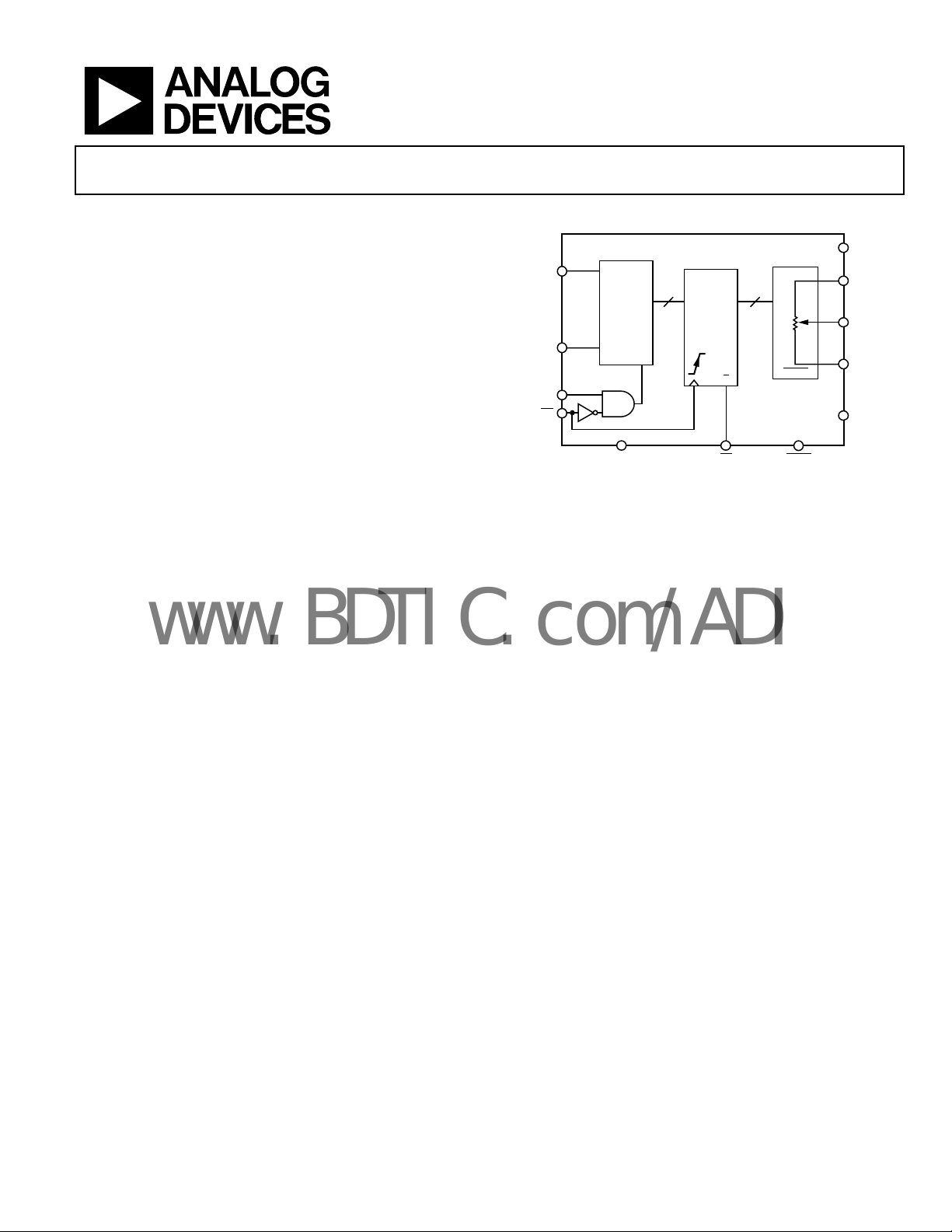
128-Position Digital Potentiometer
AD7376
FUNCTIONAL BLOCK DIAGRAM
AD7376
SDO
SDI
CLK
CS
Q
7-BIT
SERIAL
REGISTER
D
CK
GND
7 7
7-BIT
LATCH
R
RS
Figure 1.
SHDN
SHDN
V
DD
A
W
B
V
SS
01119-001
GENERAL DESCRIPTION
The AD73761 is one of the few high voltage, high performance
digital potentiometers
as a programmable resistor or resistor divider. The AD7376
performs the same electronic adjustment function as mechanical
potentiometers, variable resistors, and trimmers with enhanced
resolution, solid-state reliability, and programmability. With
digital rather than manual control, the AD7376 provides layout
flexibility and allows closed-loop dynamic controllability.
1
Patent number: 54952455.
2
The terms digital potentiometer and RDAC are used interchangeably.
2
on the market. This device can be used
The AD7376 features sleep-mode programmability in shutdown
th
at can be used to program the preset before device activation,
thus providing an alternative to costly EEPROM solutions.
The AD7376 is available in 14-lead TSSOP and 16-lead wide
dy SOIC packages in 10 kΩ, 50 kΩ, and 100 kΩ options. All
bo
parts are guaranteed to operate over the −40°C to +85°C
extended industrial temperature range.
Rev. B
Information furnished by Analog Devices is believed to be accurate and reliable. However, no
responsibility is assumed by Anal og Devices for its use, nor for any infringements of patents or ot her
rights of third parties that may result from its use. Specifications subject to change without notice. No
license is granted by implication or otherwise under any patent or patent rights of Analog Devices.
Trademarks and registered trademarks are the property of their respective owners.
One Technology Way, P.O. Box 9106, Norwood, MA 02062-9106, U.S.A.
Tel: 781.329.4700 www.analog.com
Fax: 781.461.3113 ©1997-2007 Analog Devices, Inc. All rights reserved.

AD7376
www.BDTIC.com/ADI
TABLE OF CONTENTS
Features.............................................................................................. 1
Applications....................................................................................... 1
Functional Block Diagram .............................................................. 1
General Description ......................................................................... 1
Revision History ............................................................................... 2
Specifications..................................................................................... 3
Electrical Characteristics—10 kΩ Version................................ 3
Electrical Characteristics—50 kΩ, 100 kΩ Versions ............... 4
Timing Specifications .................................................................. 5
3-Wire Digital Interface................................................................... 6
Absolute Maximum Ratings............................................................ 7
ESD Caution.................................................................................. 7
Pin Configurations and Function Descriptions ........................... 8
Typical Performance Characteristics ............................................. 9
Theory of Operation ...................................................................... 12
Programming the Variable Resistor......................................... 12
Programming the Potentiometer Divider............................... 13
3-Wire Serial Bus Digital Interface.......................................... 13
Daisy-Chain Operation ............................................................. 14
ESD Protection ........................................................................... 14
Terminal Voltage Operating Range ......................................... 14
Power-Up and Power-Down Sequences.................................. 14
Layout and Power Supply Biasing............................................ 15
Applications Information.............................................................. 16
High Voltage DAC...................................................................... 16
Programmable Power Supply ................................................... 16
Audio Volume Control .............................................................. 17
Outline Dimensions....................................................................... 18
Ordering Guide .......................................................................... 19
REVISION HISTORY
3/07—Rev. A to Rev. B
Updated Format..................................................................Universal
Changes to Absolute Maximum Ratings....................................... 7
Changes to ESD Protection Section............................................. 14
Changes to Ordering Guide.......................................................... 19
11/05—Rev. 0 to Rev. A
pdated Format..................................................................Universal
U
Deleted DIP Package..........................................................Universal
Changes to Features.......................................................................... 1
Separated Electrical Characteristics into Table 1 and Table 2 .... 3
Separated Interface Timing into Table 3 ....................................... 5
Changes to Table 1 Through Table 3.............................................. 3
Added Table 4.................................................................................... 6
Added Figure 2.................................................................................. 6
Changes to Absolute Maximum Ratings Section......................... 7
Deleted Parametric Test Circuits Section...................................... 7
Changes to Typical Performance Characteristics......................... 9
Added Daisy-Chain Operation Section....................................... 14
Added ESD Protection Section..................................................... 14
Added Terminal Voltage Operating Range Section................... 14
Added Power-Up and Power-Down Sequences Section ........... 14
Added Layout and Power Supply Biasing Section...................... 15
Added Applications Section .......................................................... 16
Updated Outline Dimensions....................................................... 18
Changes to Ordering Guide.......................................................... 19
10/97—Revision 0: Initial Version
Rev. B | Page 2 of 20

AD7376
www.BDTIC.com/ADI
SPECIFICATIONS
ELECTRICAL CHARACTERISTICS—10 kΩ VERSION
VDD/VSS = ±15 V ± 10%, VA = VDD, VB = VSS/0 V, −40°C < TA < +85°C, unless otherwise noted.
Table 1.
Parameter Symbol Conditions Min Typ1Max Unit
DC CHARACTERISTICS—
RHEOSTAT MODE
Resistor Differential Nonlinearity2R-DNL RWB, VA = NC, VDD/VSS = ±15 V −1 ±0.5 +1 LSB
Resistor Nonlinearity
2
Nominal Resistor Tolerance ∆RAB T
Resistance Temperature Coefficient3(∆RAB/RAB)/∆T × 106 V
Wiper Resistance RW V
DC CHARACTERISTICS—
POTENTIOMETER DIVIDER MODE
Integral Nonlinearity
Differential Nonlinearity
4
4
Voltage Divider Temperature
Coefficient
Full-Scale Error V
Zero-Scale Error V
RESISTOR TERMINALS
Voltage Range
5
Capacitance6 A, B C
Capacitance
Shutdown Supply Current
6
7
Shutdown Wiper Resistance R
Common-Mode Leakage ICM V
DIGITAL INPUTS AND OUTPUTS
Input Logic High VIH V
Input Logic Low VIL V
Output Logic High VOH R
Output Logic Low VOL I
Input Current IIL V
Input Capacitance
6
POWER SUPPLIES
Power Supply Range VDD/VSS Dual-supply range ±4.5 ±16.5 V
Power Supply Range VDD Single-supply range, VSS = 0 4.5 33 V
Positive Supply Current IDD V
V
Negative Supply Current ISS V
V
Power Dissipation
8
Power Supply Rejection Ratio PSRR ΔVDD/ΔVSS = ±15 V ± 10% −0.2 ±0.05 +0.2 %/%
R-INL RWB, VA = NC, VDD/VSS = ±15 V −1 ±0.5 +1 LSB
= 25°C −30 +30 %
A
= VDD, wiper = no connect −300 ppm/°C
AB
= ±15 V 120 200 Ω
DD/VSS
VDD/VSS = ±5 V 260 Ω
INL VDD/VSS = ±15 V −1 ±0.5 +1 LSB
DNL VDD/VSS = ±15 V −1 ±0.5 +1 LSB
(∆V
V
CW
I
)/∆T × 106 Code = 0x40 5 ppm/°C
W/VW
Code = 0x7F, VDD/VSS = ±15 V −3 −1.5 0 LSB
WFSE
Code = 0x00, VDD/VSS = ±15 V 0 1.5 3 LSB
WZSE
V
A, B, W
A, B
f = 1 MHz, measured to GND,
ode = 0x40
c
f = 1 MHz, measured to GND,
ode = 0x40
c
A_SD
W_SD
= VDD, VB = 0 V, SHDN = 0
V
A
= VDD, VB = 0 V, SHDN = 0, VDD = 15 V
V
A
= VB = VW 1 nA
A
= 5 V or 15 V 2.4 V
DD
= 5 V or 15 V 0.8 V
DD
= 2.2 kΩ to 5 V 4.9 V
Pull-Up
= 1.6 mA, V
OL
= 0 V or 5 V ±1 μA
IN
= 5 V, VDD = 15 V 0.4 V
LOGI C
VDD V
SS
45 pF
60 pF
0.02 1 μA
170 400 Ω
CIL 5 pF
= 5 V or VIL = 0 V, VDD/VSS = ±15 V 2 mA
IH
= 5 V or VIL = 0 V, VDD/VSS = ±5 V 12 25 μA
IH
= 5 V or VIL = 0 V, VDD/VSS = ±15 V −0.1 mA
IH
= 5 V or VIL = 0 V, VDD/VSS = ±5 V −0.1 mA
IH
P
V
DISS
= 5 V or VIL = 0 V, VDD/VSS = ±15 V 31.5 mW
IH
Rev. B | Page 3 of 20

AD7376
www.BDTIC.com/ADI
Parameter Symbol Conditions Min Typ1Max Unit
DYNAMIC CHARACTERISTICS
Bandwidth −3 dB BW Code = 0x40 470 kHz
Total Harmonic Distortion THDW V
VW Settling Time tS V
Resistor Noise Voltage e
1
Typical values represent average readings at 25°C, VDD = 15 V, and VSS = −15 V.
2
Resistor position nonlinearity error R-INL is the deviation from an ideal value measured between the maximum and minimum resistance wiper positions. R-DNL
measures the relative step change from an ideal value measured between successive tap positions. Parts are guaranteed monotonic.
3
Pb-free parts have a 35 ppm/°C temperature coefficient (tempco).
4
INL and DNL are measured at VW with the RDAC configured as a potentiometer divider, similar to a voltage output digital-to-analog converter. VA = VDD and VB = 0 V.
DNL specification limits of ±1 LSB maximum are guaranteed monotonic operating conditions.
5
Resistor Terminals A, B, and W have no limitations on polarity with respect to each other.
6
Guaranteed by design and not subject to production test.
7
Measured at the A terminal. A terminal is open circuit in shutdown mode.
8
P
is calculated from (IDD × VDD) + abs(ISS × VSS). CMOS logic level inputs result in minimum power dissipation.
DISS
9
Bandwidth, noise, and settling times are dependent on the terminal resistance value chosen. The lowest R value results in the fastest settling time and highest
bandwidth. The highest R value results in the minimum overall power consumption.
10
All dynamic characteristics use VDD = 15 V and VSS = −15 V.
ELECTRICAL CHARACTERISTICS—50 kΩ, 100 kΩ VERSIONS
VDD/VSS = ±15 V ± 10% or ±5 V ± 10%, VA = VDD, VB = VSS/0 V, −40°C < TA < +85°C, unless otherwise noted.
Table 2.
Parameter Symbol Conditions Min Typ1Max Unit
DC CHARACTERISTICS—RHEOSTAT MODE
Resistor Differential Nonlinearity
Resistor Nonlinearity
R
Nominal Resistor Tolerance ∆RAB T
Resistance Temperature Coefficient
Wiper Resistance RW V
DC CHARACTERISTICS—
POTENTIOMETER DIVIDER MODE
Integral Nonlinearity
Differential Nonlinearity
Voltage Divider Temperature
Coefficient
Full-Scale Error V
Zero-Scale Error V
RESISTOR TERMINALS
Voltage Range
Capacitance6 A, B C
Capacitance
Shutdown Supply Current
Shutdown Wiper Resistance R
Common-Mode Leakage ICM V
5
6
6, 9 ,10
2
= 1 V rms, VB = 0 V, f = 1 kHz 0.006 %
A
= 10 V, VB = 0 V, ±1 LSB error band 4 μs
A
R
N_WB
2
R-DNL RWB, VA = NC −1 ±0.5 +1 LSB
= 5 kΩ, f = 1 kHz 0.9 nV√Hz
WB
R-INL RWB, VA = NC, RAB = 50 kΩ −1.5 ±0.5 +1.5 LSB
, VA = NC, RAB = 100 kΩ −1 ±0.5 +1 LSB
WB
= 25°C −30 +30 %
3
(∆RAB/RAB)/∆T ×
6
10
A
= VDD, wiper = no connect −300 ppm/°C
V
AB
= ±15 V 120 200 Ω
DD/VSS
VDD/VSS = ±5 V 260 Ω
4
4
7
INL −1 ±0.5 +1 LSB
DNL −1 ±0.5 +1 LSB
(∆V
)/∆T × 106 Code = 0x40 5 ppm/°C
W/VW
Code = 0x7F −2 −0.5 0 LSB
WFSE
Code = 0x00 0 0.5 1 LSB
WZSE
V
V
A, B, W
CW
I
A_SD
A, B
W_SD
f = 1 MHz, measured to GND,
ode = 0x40
c
f = 1 MHz, measured to GND,
ode = 0x40
c
= VDD, VB = 0 V, SHDN = 0
V
A
= VDD, VB = 0 V, SHDN = 0, VDD = 15 V
V
A
= VB = VW 1 nA
A
VDD V
SS
45 pF
60 pF
0.02 1 μA
170 400 Ω
Rev. B | Page 4 of 20
AD7376
www.BDTIC.com/ADI
Parameter Symbol Conditions Min Typ1Max Unit
DIGITAL INPUTS AND OUTPUTS
Input Logic High VIH V
Input Logic Low VIL V
Output Logic High VOH R
Output Logic Low VOL I
Input Current IIL V
Input Capacitance
6
CIL 5 pF
POWER SUPPLIES
Power Supply Range VDD/VSS Dual-supply range ±4.5 ±16.5 V
Power Supply Range VDD Single-supply range, VSS = 0 4.5 33 V
Positive Supply Current IDD V
V
Negative Supply Current ISS V
V
Power Dissipation
8
P
V
DISS
Power Supply Rejection Ratio PSRR −0.25 ±0.1 +0.25 %/%
DYNAMIC CHARACTERISTICS
6, 9 , 10
Bandwidth −3 dB BW RAB = 50 kΩ, code = 0x40 90 kHz
R
Total Harmonic Distortion THDW V
VW Settling Time tS V
Resistor Noise Voltage e
1
Typical values represent average readings at 25°C, VDD = 15 V, and VSS = −15 V.
2
Resistor position nonlinearity error R-INL is the deviation from an ideal value measured between the maximum and minimum resistance wiper positions. R-DNL
measures the relative step change from an ideal value measured between successive tap positions. Parts are guaranteed monotonic.
3
Pb-free parts have a 35 ppm/°C temperature coefficient.
4
INL and DNL are measured at VW with the RDAC configured as a potentiometer divider, similar to a voltage output digital-to-analog converter. VA = VDD and VB = 0 V.
DNL specification limits of ±1 LSB maximum are guaranteed monotonic operating conditions.
5
Resistor Terminals A, B, and W have no limitations on polarity with respect to each other.
6
Guaranteed by design and not subject to production test.
7
Measured at the A terminal. A terminal is open circuit in shutdown mode.
8
P
is calculated from (IDD × VDD) + abs(ISS × VSS). CMOS logic level inputs result in minimum power dissipation.
DISS
9
Bandwidth, noise, and settling times are dependent on the terminal resistance value chosen. The lowest R value results in the fastest settling time and highest
bandwidth. The highest R value results in the minimum overall power consumption.
10
All dynamic characteristics use VDD = 15 V and VSS = −15 V.
R
N_WB
TIMING SPECIFICATIONS
= 5 V or 15 V 2.4 V
DD
= 5 V or 15 V 0.8 V
DD
= 2.2 kΩ to 5 V 4.9 V
Pull-Up
= 1.6 mA, V
OL
= 0 V or 5 V ±1 μA
IN
= 5 V or VIL = 0 V, VDD/VSS = ±15 V 2 mA
IH
= 5 V or VIL = 0 V, VDD/VSS = ±5 V 12 25 μA
IH
= 5 V or VIL = 0 V, VDD/VSS = ±15 V −0.1 mA
IH
= 5 V or VIL = 0 V, VDD/VSS = ±5 V −0.1 mA
IH
= 5 V or VIL = 0 V, VDD/VSS = ±15 V 31.5 mW
IH
= 100 kΩ, code = 0x40 50 kHz
AB
= 1 V rms, VB = 0 V, f = 1 kHz 0.002 %
A
= 10 V, VB = 0 V, ±1 LSB error band 4 μs
A
= 25 kΩ, f = 1 kHz 2 nV√Hz
WB
= 5 V, VDD = 15 V 0.4 V
LOGI C
Table 3.
Parameter Symbol Conditions Min Typ Max Unit
INTERFACE TIMING CHARACTERISTICS
Clock Frequency f
1, 2
CLK
Input Clock Pulse Width tCH, tCL Clock level high or low 120 ns
Data Setup Time tDS 30 ns
Data Hold Time tDH 20 ns
CLK to SDO Propagation Delay
CS Setup Time
CS High Pulse Width
3
tPD R
t
120 ns
CSS
t
150 ns
CSW
= 2.2 kΩ, CL < 20 pF 10
Pull-Up
Reset Pulse Width tRS 120 ns
t
CLK Fall to CS Fall Hold Time
CLK Rise to CS Rise Hold Time
CS Rise to Clock Rise Setup
1
Guaranteed by design and not subject to production test.
2
See for the location of the measured values. All input control voltages are specified with tR = tF = 1 ns (10% to 90% of VDD) and timed from a voltage level of 1.6 V.
Figure 3
Switching characteristics are measured using VDD = 15 V and VSS = −15 V.
3
Propagation delay depends on value of VDD, R
Pull-Up
10 ns
CSH0
t
120 ns
CSH
t
120 ns
CS1
, and CL.
Rev. B | Page 5 of 20
4 MHz
100 ns
AD7376
www.BDTIC.com/ADI
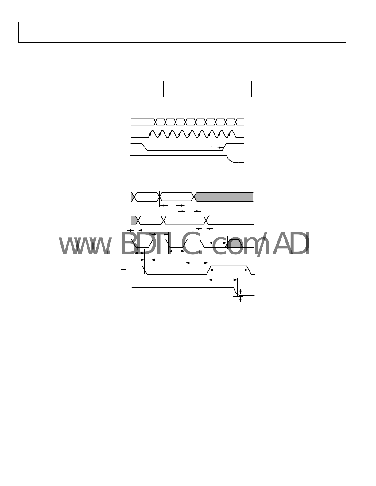
3-WIRE DIGITAL INTERFACE
Table 4. AD7376 Serial Data-Word Format
1
MSB LSB
D6 D5 D4 D3 D2 D1 D0
6
2
1
Data is loaded MSB first.
2
0
1
CLK
V
SDI
OUT
CS
0
1
0
1
0
1
0
D6 D5 D4 D3 D2 D1 D0
RDAC REGISTER LOAD
01119-002
Figure 2. AD7376 3-Wire Digital Interface Timing Diagram
= VDD, VB = 0 V, VW = V
(V
A
OUT
)
1
SDI
(DATA IN)
SDO
(DATA OUT)
CLK
CS
V
OUT
t
V
CSH0
DD
0V
D
0
1
0
1
0
1
0
X
D'
X
t
CH
t
CSS
D
X
t
DS
t
DH
D'
X
t
PD_MAX
t
CS1
t
CL
t
CSH
t
CSW
t
S
±1 LSB ER ROR BAND
±1 LSB
01119-003
Figure 3. Detail Timing Diagram
Rev. B | Page 6 of 20

AD7376
www.BDTIC.com/ADI
ABSOLUTE MAXIMUM RATINGS
TA = 25°C, unless otherwise noted.
Table 5.
Parameter Rating
VDD to GND −0.3 V to +35 V
VSS to GND +0.3 V to −16.5 V
VDD to VSS −0.3 V to +35 V
VA, VB, VW to GND VSS to VDD
Maximum Current
IWB, IWA Pulsed ±20 mA
IWB Continuous (RWB ≤ 6 kΩ, A open,
V
= 30 V/0 V)
DD/VSS
IWA Continuous (RWA ≤ 6 kΩ, B open,
= 30 V/0 V)
V
DD/VSS
Digital Input and Output Voltages to GND 0 V to VDD + 0.3 V
Operating Temperature Range −40°C to +85°C
Maximum Junction Temperature (T
Storage Temperature Range −65°C to +150°C
Reflow Soldering
Peak Temperature 260°C
Time at Peak Temperature 20 sec to 40 sec
Package Power Dissipation (T
Thermal Resistance θJA
16-Lead SOIC_W 120°C/W
14-Lead TSSOP 240°C/W
1
Maximum terminal current is bound by the maximum current handling of
the switches, maximum power dissipation of the package, and maximum
applied voltage across any two of the A, B, and W terminals at a given
resistance.
2
Package power dissipation = (T
1
1
JMAX
– TA)/θJA.
JMAX
±5 mA
±5 mA
2
)
150°C
− TA)/θJA
JMAX
Stresses above those listed under Absolute Maximum Ratings
may cause permanent damage to the device. This is a stress
rating only; functional operation of the device at these or any
other conditions above those indicated in the operational
section of this specification is not implied. Exposure to absolute
maximum rating conditions for extended periods may affect
device reliability.
ESD CAUTION
Rev. B | Page 7 of 20

AD7376
www.BDTIC.com/ADI
PIN CONFIGURATIONS AND FUNCTION DESCRIPTIONS
A 1
A
1
B
2
V
3
SS
GND
4
CS
5
RS
6
CLK
7
NC = NO CONNECT
AD7376
TOP VIEW
(Not to Scale)
W
14
13
NC
12
V
DD
11
SDO
10
SHDN
9
SDI
8
NC
01119-004
Figure 4. 14-Lead TSSOP Pin Configuration
B 2
3
V
SS
GND 4
CLK
AD7376
TOP VIEW
(Not to Scale)
CS 5 SHDN12
RS 6 SDI11
7
NC 8 NC9
NC = NO CONNECT
Figure 5. 16-Lead SOIC_W Pin Configuration
Table 6.Pin Function Descriptions
Pin No.
14-Lead
TSSOP
16-Lead
SOL Mnemonic Description
1 1 A A Terminal. VSS ≤ VA ≤ VDD.
2 2 B B Terminal. VSS ≤ VB ≤ VDD.
3 3 VSS Negative Power Supply.
4 4 GND Digital Ground.
5 5
6 6
CS
RS
Chip Select Input, Active Low. When CS returns high, data is loaded into the wiper register.
Reset to Midscale.
7 7 CLK Serial Clock Input. Positive edge triggered.
8 8, 9, 10 NC No Connect. Let it float or ground.
9 11 SDI Serial Data Input (data loads MSB first).
10 12
Shutdown. A terminal open ended; W and B terminals shorted. Can be used as
SHDN
programmable preset.
1
11 13 SDO Serial Data Output.
12 14 VDD Positive Power Supply.
13 15 NC No Connect. Let it float or ground.
14 16 W Wiper Terminal. VSS ≤ VW ≤ VDD.
1
Assert shutdown and program the device during power-up. Then, deassert the shutdown to achieve the desirable preset level.
W16
NC15
14
V
DD
SDO13
10
NC
01119-005
Rev. B | Page 8 of 20

AD7376
A
A
www.BDTIC.com/ADI
TYPICAL PERFORMANCE CHARACTERISTICS
0.5
0.4
0.3
0.2
0.1
0
T MODE INL (LSB)
–40°C
–0.1
–0.2
RHEOST
–0.3
–0.4
–0.5
0 12816 32 48 64 80 96 112
+85°C
+25°C
CODE (Decimal)
VDD = +15V
V
= –15V
SS
Figure 6. Resistance Step Position Nonlinearity Error vs. Code
01119-006
0.5
0.4
0.3
POTENTI OMETER MO DE DNL (LSB)
0.2
0.1
–0.1
–0.2
–0.3
–0.4
–0.5
+85°C
+25°C
0
0 12816 32 48 64 80 96 112
CODE (Decimal)
–40°C
VDD = +15V
V
= –15V
SS
Figure 9. Potentiometer Divider Differential Nonlinearity Error vs. Code
01119-009
0.5
0.4
0.3
0.2
0.1
0
T MODE DNL (LSB)
–0.1
–0.2
RHEOST
–0.3
–0.4
–0.5
0 12816 32 48 64 80 96 112
+85°C
+25°C
CODE (Decimal)
–40°C
VDD = +15V
V
= –15V
SS
Figure 7. Relative Resistance Step Change from Ideal vs. Code
0.5
0.4
0.3
0.2
0.1
0
–40°C
–0.1
–0.2
–0.3
POTENTI OMETER MO DE INL (LSB)
–0.4
–0.5
0 12816 32 48 64 80 96 112
+85°C
+25°C
CODE (Decimal)
VDD = +15V
V
= –15V
SS
Figure 8. Potentiometer Divider Nonlinearity Error vs. Code
20
16
12
8
4
SUPPLY CURRENT (µA)
0
01119-007
–4
–40
Figure 10. Supply Current (I
0.5
0.4
0.3
0.2
0.1
0
–0.1
–0.2
SHUTDOWN CURRENT ( µA)
–0.3
–0.4
01119-008
–0.5
–40
IDD @ VDD/VSS = 30V/0V
IDD @ VDD/VSS = ±15V
ISS @ VDD/VSS = 30V/0V
ISS @ VDD/VSS = ±15V
–20 0 20 40 60 80 100 120
TEMPERATURE (°C)
, ISS) vs. Temperature
DD
–20 0 20 40 60 80 100 120
TEMPERATURE (ºC)
01119-010
01119-011
Figure 11. Shutdown Current vs. Temperature
Rev. B | Page 9 of 20

AD7376
A
www.BDTIC.com/ADI
120
100
(kΩ)
AB
80
60
40
TOTAL RESISTANCE, R
20
0
–40
–20 0 20 40 60 80 100 120
100kΩ
50kΩ
10kΩ
TEMPERATURE (°C)
Figure 12. Total Resistance vs. Temperature
350
(Ω)
W
WIPER RESISTANCE R
300
250
200
150
100
50
0
–40
–20 0 20 40 60 80 100 120
RW @ VDD/VSS = ±5V
RW @ VDD/VSS = ±15V
TEMPERATURE (°C)
Figure 13. Wiper Contact Resistance vs. Temperature
VDD/VSS = ±15V
120
100
80
60
40
20
T MODE TEMPCO (ppm/°C)
0
RHEOST
–20
01119-012
–40
0
–6
–12
–18
–24
–30
(dB)
–36
–42
–48
–54
01119-013
–60
100kΩ
10kΩ
50kΩ
0 12816 32 48 64 80 96 112
Figure 15. (ΔV
0x40
0x20
0x10
0x08
0x04
0x02
0x01
1k
CODE (Decimal)
)/ΔT Potentiometer Mode Tempco
WB/VWB
10k 100k
(Hz)
Figure 16. 10 kΩ Gain vs. Frequency vs. Code
VDD/VSS = ±15V
1M
01119-015
01119-016
120
100
80
60
40
20
0
–20
POTENTI OMETER MO DE TEMPCO ( ppm/°C)
–40
0 12816 32 48 64 80 96 112
Figure 14. (ΔR
100kΩ
10kΩ
50kΩ
CODE (Decimal)
)/ΔT Rheostat Mode Tempco
WB/RWB
VDD/VSS = ±15V
01119-014
0
0x40
–6
0x20
–12
0x10
–18
0x08
–24
0x04
–30
(dB)
0x02
–36
0x01
–42
–48
–54
–60
1k 1M
10k 100k
Figure 17. 50 kΩ Gain vs. Frequency vs. Code
Rev. B | Page 10 of 20
(Hz)
01119-017

AD7376
A
www.BDTIC.com/ADI
THD + N (%)
0.001
0.0001
0.1
0.01
100kΩ
10
FREQUENCY (Hz)
VDD/VSS = ±15V
CODE = MIDSCALE
= 1Vrms
V
IN
10kΩ
50kΩ
Figure 21. Total Harmonic Distortion Plus Noise vs. Frequency
01119-021
100k100 1k 10k
0
0x40
–6
0x20
–12
0x10
–18
0x08
–24
0x04
–30
(dB)
0x02
–36
0x01
–42
–48
–54
–60
1k
10k 100k
(Hz)
Figure 18. 100 kΩ Gain vs. Frequency vs. Code
1M
01119-018
1
2
0.1
VDD/VSS = ±15V
CODE = MIDSCALE
= 1kHz
f
IN
10kΩ
1
CH1 5V CH2 5V M2µs A CH1 4.20V
T 50%
Figure 19. Midscale to Midscale − 1 Transition Glitch
80
CODE = 40H, VA = VDD, VB = V
60
40
PSRR (–dB)
–PSRR @ VDD/VSS = ±5V
DC ± 10% p-p AC
20
0
100 1M
1k 10k 100k
Figure 20. Power Supply R
SS
–PSRR @ VDD/VSS = ±15V
DC ± 10% p-p AC
+PSRR @ VDD/VSS = ±15V
DC ± 10% p-p AC
+PSRR @ VDD/VSS = ±5V
DC ± 10% p-p AC
FREQUENCY (Hz)
ejection vs. Frequency
THD + N (%)
0.01
01119-019
0.001
0.001
AMPLI TUDE (V )
50kΩ
100kΩ
01119-022
100.01 0.1 1
Figure 22. Total Harmonic Distortion Plus Noise vs. Amplitude
6
5
(mA)
4
WB_MAX
3
L I
2
THEORETIC
1
01119-020
0
RAB = 100kΩ
0116 32 48 64 80 96 112
RAB = 10kΩ
RAB = 50kΩ
CODE (Decimal)
VDD/VSS = 30V/0V
V
= V
A
DD
VB = 0V
01119-023
28
Figure 23. Theoretical Maximum Current vs. Code
Rev. B | Page 11 of 20

AD7376
−
www.BDTIC.com/ADI
THEORY OF OPERATION
PROGRAMMING THE VARIABLE RESISTOR
Rheostat Operation
The part operates in rheostat mode when only two terminals
are used as a variable resistor. The unused terminal can be left
floating or tied to the W terminal as shown in Figure 24.
A
W
B
Figure 24. Rheostat Mode Configuration
The nominal resistance between Terminals A and B, RAB, is
available in 10 kΩ, 50 kΩ, and 100 kΩ with ±30% tolerance and
has 128 tap points accessed by the wiper terminal. The 7-bit
data in the RDAC latch is decoded to select one of the 128
possible settings. Figure 25 shows a simplified RDAC structure.
SHDN
D6
D5
D4
D3
D2
D1
D0
RDAC
LATCH
AND
DECODER
Figure 25. AD7376 Equivalent RDAC Circuit
The general equation determining the digitally programmed
output resistance between the W and the B terminals is
WB
128
D
DR +×=
)(
where:
D is the decimal equivalent of the binary code loaded in the
7-bit RDAC register from 0 to 127.
R
is the end-to-end resistance.
AB
R
is the wiper resistance contributed by the on resistance of
W
the internal switch.
A
W
B
R
S
R
S
R
S
R
S
AB
0x7F
0x01
RS = R
NOMINAL
(1)
RR
W
0x00
SW
A
W
B
A
SW
B
/128
01119-024
A
W
B
01119-025
The AD7376 wiper switches are designed with the transmission
gate CMOS topology, and the gate voltage is derived from the
. Each switch’s on resistance, RW, is a function of VDD and
V
DD
temperature (see Figure 13).
Contrary to the temperature coefficient of R
, the temperature
AB
coefficient of the wiper resistance is significantly higher because
the wiper resistance doubles with every 100° increase. As a result,
the user must take into consideration the contribution of R
W
on
the desirable resistance. On the other hand, each switch’s on
resistance is insensitive to the tap point potential and remains
relatively flat at 120 Ω typical at a V
of 15 V and a
DD
temperature of 25°C.
Assuming that a 10 kΩ part is used, the wiper’s first connection
starts at the B terminal for programming code 0x00, where SW
is closed. The minimum resistance between Terminals W and B
is therefore 120 Ω in general. The second connection is the first
R
tap point, which corresponds to 198 Ω (
= 1/128 × RAB + RW
WB
= 78 Ω + 120 Ω) for programming code 0x01, and so on.
Each LSB data value increase moves the wiper up the resistor
R
ladder until the last tap point is reached at 10,042 Ω (
R
). Regardless of which settings the part is operating with, care
W
– 1 LSB +
AB
should be taken to limit the current conducted between any A
and B, W and A, or W and B terminals to a maximum dc
current of 5 mA and a maximum pulse current of 20 mA.
Otherwise, degradation or possible destruction of the internal
switch contact can occur.
Similar to the mechanical potentiometer, the resistance of the
RDAC between the W and A terminals also produces a digitally
controlled complementary resistance,
R
.
WA
When these terminals are used, the B terminal can be opened.
Setting the resistance value for R
starts at a maximum value
WA
of resistance and decreases as the data loaded into the latch
increases in value. The general equation for this operation is
128
DR +×
=
)(
D
128
ABWA
(2)
RR
W
B
Rev. B | Page 12 of 20

AD7376
www.BDTIC.com/ADI
PROGRAMMING THE POTENTIOMETER DIVIDER
Voltage Output Operation
The digital potentiometer easily generates a voltage divider at
Wiper W to Terminal B and Wiper W to Terminal A that is
proportional to the input voltage at Terminal A to Terminal B.
Unlike the polarity of V
voltage across Terminal A to Terminal B, Wiper W to Terminal A,
and Wiper W to Terminal B can be at either polarity.
Figure 26. Potentiometer Mode Configuration
If ignoring the effect of the wiper resistance for the purpose of
approximation, connecting the Terminal A to 30 V and the
Terminal B to ground produces an output voltage at the Wiper W
to Terminal B ranging from 0 V to 1 LSB less than 30 V. Each
LSB of voltage is equal to the voltage applied across Terminals A
and B divided by the 128 positions of the potentiometer divider.
The general equation defining the output voltage at V
respect to ground for any valid input voltage applied to
Terminals A and B is
W
128
D
DV
)( =
A more accurate calculation that includes the effect of wiper
re
sistance, V
, is
W
WB
DV
)( +=
W
R
Operation of the digital potentiometer in the divider mode
re
sults in a more accurate operation over temperature. Unlike
when in rheostat mode, the output voltage in divider mode is
primarily dependent on the ratio, not the absolute values, of the
internal resistors R
reduces to 5 ppm/°C.
to GND, which must be positive,
DD
V
I
A
W
V
O
B
01119-026
with
W
(3)
V
A
DR
DR
)(
V
A
AB
and RWB. Therefore, the temperature drift
WA
WA
)(
V
(4)
R
B
AB
3-WIRE SERIAL BUS DIGITAL INTERFACE
The AD7376 contains a 3-wire digital interface (CS, CLK, and
SDI). The 7-bit serial word must be loaded MSB first. The
format of the word is shown in
ensitive CLK input requires clean transitions to avoid clocking
s
incorrect data into the serial input register. Standard logic
families work well. When
serial register upon each positive clock edge.
The data setup and hold times in Tabl e 3 determine the valid
g requirements. The AD7376 uses a 7-bit serial input data
timin
register word that is transferred to the internal RDAC register
when the
CS
line returns to logic high. Extra MSB bits are
ignored.
The AD7376 powers up at a random setting. However, the
mids
cale preset or any desirable preset can be achieved by
RS
manipulating
When the reset (
SHDN
or
RS
) pin is asserted, the wiper resets to the
midscale value. Midscale reset can be achieved dynamically or
during power-up if an extra I/O is used.
When the
SHDN
pin is asserted, the AD7376 opens SWA to let
the Terminal A float and to short Wiper W to Terminal B. The
AD7376 consumes negligible power during the shutdown mode
and resumes the previous setting once the
On the other hand, the AD7376 can be programmed with any
settings during shutdown. With an extra programmable I/O
asserting shutdown during power-up, this unique feature allows
the AD7376 with programmable preset at any desirable level.
Table 7 shows the logic truth table for all operations.
Table 7. Input Logic Control Truth Table
CS
CLK
L L H H Enables SR, enables SDO pin.
P L H H
X P H H Loads SR data into 7-bit RDAC latch.
X H H H No operation.
X X L H
X H P H Latches 7-bit RDAC latch to 0x40.
X H H L
1
P = positive edge, X = don’t care, and SR = shift register.
RS SHDN
Figure 2. The positive edge-
CS
is low, the clock loads data into the
with an extra I/O.
pin is released.
SHDN
1
Register Activity
Shifts one bit in from the SDI pin. The
enth previously entered bit is
sev
shifted out of the SDO pin.
Sets 7-bit RDAC latch to midscale,
entered, and SDO latch cleared.
wiper c
Opens circuits resistor of Terminal A,
onnects Wiper W to Terminal B,
c
turns off SDO output transistor.
Rev. B | Page 13 of 20

AD7376
V
V
V
www.BDTIC.com/ADI
DAISY-CHAIN OPERATION
SHDN
CS
SDI
CLK
RS
SERIAL
REGISTER
Figure 27. Detailed SDO Output Sch
D
CKQRS
ematic of the AD7376
Figure 27 shows the details of the serial data output pin (SDO).
SDO shifts out the SDI content in the previous frame; therefore,
it can be used for daisy-chaining multiple devices. The SDO pin
contains an open-drain N-Channel MOSFET and requires a
pull-up resistor if the SDO function is used.
Users need to tie the SDO pin of one package to the SDI pin of
he next package. For example, in Figure 28, if two AD7376s are
t
d
aisy-chained, a total of 14 bits of data are required for each
operation. The first set of seven bits goes to U2; the second set
of seven bits goes to U1.
CS
should be kept low until all 14 bits
are clocked into their respective serial registers. Then
pulled high to complete the operation.
When daisy-chaining multiple devices, users may need to
in
crease the clock period because the pull-up resistor and the
capacitive loading at the SDO to SDI interface may induce a
time delay to subsequent devices.
U1 U2
µC
MOSI
SSSCLK
AD7376
SDOSDI
CLKCS
DD
R
PU
2.2kΩ
AD7376
SDI
CS
CS
SDO
CLK
is
SDO
01119-027
ESD PROTECTION
All digital inputs are protected with a series input resistor and
an ESD structure shown in Figure 29. These structures apply to
igital input pins
d
CS
, CLK, SDI, RS, and
INPUT
LOGIC
PINS
Figure 29. Equivalent ESD Protection Circuit
340Ω
SHDN
DD
GND
.
01119-029
All analog terminals are also protected by ESD protection
diodes, as shown in Figure 30.
DD
A
W
B
V
01119-030
SS
Figure 30. Equivalent ESD Protection Analog Pins
TERMINAL VOLTAGE OPERATING RANGE
The AD7376 VDD and VSS power supplies define the boundary
conditions for proper 3-terminal digital potentiometer operation. Applied signals present on Terminals A, B, and W that
are more positive than V
clamped by the internal forward-biased diodes (see Figure 30).
or more negative than VSS will be
DD
POWER-UP AND POWER-DOWN SEQUENCES
Because of the ESD protection diodes that limit the voltage
Figure 28. Daisy-Chain Configuration
01119-028
compliance at Terminals A, B, and W (see Figure 30), it is
i
mportant to power V
DD/VSS
Terminals A, B, and W. Otherwise, the diodes are forward
biased such that V
the system. Similarly, V
are powered unintentionally and affect
DD/VSS
DD/VSS
The ideal power-up sequence is in the following order: GND,
V
, VSS, digital inputs, and VA/VB/VW. The order of powering
DD
, VB, VW, and the digital inputs is not important, as long as
V
A
they are powered after V
Rev. B | Page 14 of 20
DD/VSS
before applying voltage to
should be powered down last.
.

AD7376
V
www.BDTIC.com/ADI
LAYOUT AND POWER SUPPLY BIASING
It is a good practice to employ a compact, minimum lead-length
layout design. The leads to the input should be as direct as
possible, with a minimum conductor length. Ground paths
should have low resistance and low inductance.
Similarly, it is also good practice to bypass the power supplies
wi
th quality capacitors. Low ESR (equivalent series resistance)
1 μF to 10 μF tantalum or electrolytic capacitors should be
applied at the supplies to minimize transient disturbances and
filter low frequency ripple.
b
ypassing configuration for the AD7376.
Figure 31 illustrates the basic supply
The ground pin of the AD7376 is a digital ground reference. To
inimize the digital ground bounce, the AD7376 digital ground
m
terminal should be joined remotely to the analog ground (see
Figure 31).
DD
+
C1
C3
10µF
0.1µF
+
C4
C2
10µF
V
SS
Figure 31. Power Supply Bypassing
0.1µF
V
DD
AD7376
V
SS
GND
01119-031
Rev. B | Page 15 of 20

AD7376
V
www.BDTIC.com/ADI
APPLICATIONS INFORMATION
HIGH VOLTAGE DAC
The AD7376 can be configured as a high voltage DAC as high
as 30 V. The circuit is shown in Figure 32. The output is
2
RD
DV
O
Where D is t
DD
R
BIAS
ADR512
D1
⎡
)(
⎢
128
⎣
⎛
1V2.1
⎜
⎝
he decimal code from 0 to 127.
V
DD
U1A
V+
AD8512
V–
R2
R1
Figure 32. High Voltage DAC
+×=
⎤
⎞
(5)
⎟
⎥
1
R
⎠
⎦
U2
AD7376
100kΩ
B
U1B
V
AD8512
OUT
PROGRAMMABLE POWER SUPPLY
With a boost regulator such as ADP1611, AD7376 can be used
as the variable resistor at the regulator’s FB pin to provide the
programmable power supply (see Figure 33). The output is
D
⎡
⎛
⎜
⎢
128
⎝
+×=
V
O
Note that the AD7376’s V
L1 acts as a short, and V
1V23.1
⎢
⎢
⎢
⎣
is derived from the output. Initially
DD
is one diode voltage drop below +5 V.
DD
The output slowly establishes to the final value.
The AD7376 shutdown sleep-mode programming can be used
t
o program a desirable preset level at power-up.
U1
AD7376
V
DD
C1
1119-032
0.1µF
A
W
R1
100kΩ
B
SD
R2
8.5kΩ
Figure 33. Programmable Power Supply
5V
C
10µF
1.23V
22nF
IN
C
SS
⎤
⎞
×
R
⎟
AB
⎥
⎠
R
(6)
⎥
2
⎥
⎥
⎦
IN
U2
ADP1611
RT
FB
SS
GND
SW
COMP
L1
4.7µF
D1
R
C
220kΩ
C
C
150pF
C
OUT
10µF
V
OUT
01119-033
Rev. B | Page 16 of 20

AD7376
E
V
www.BDTIC.com/ADI
AUDIO VOLUME CONTROL
Because of its good THD performance and high voltage
capability, the AD7376 can be used for digital volume control. If
AD7376 is used directly as an audio attenuator or gain amplifier,
a large step change in the volume level at any arbitrary time can
lead to an abrupt discontinuity of the audio signal, causing an
audible zipper noise. To prevent this, a zero-crossing window
detector can be inserted to the
update until the audio signal crosses the window. Since the
input signal can operate on top of any dc levels rather than
absolute zero volt level, zero-crossing, in this case, means the
signal is ac-coupled and the dc offset level is the signal zero
reference point.
The configuration to reduce zipper noise and the result of using
his configuration are shown in Figure 35 and Figure 34,
t
spectively. The input is ac-coupled by C1 and attenuated
re
down before feeding into the window comparator formed by
U2, U3, and U4B. U6 is used to establish the signal zero
reference. The upper limit of the comparator is set above its
offset and, therefore, the output pulses high whenever the input
falls between 2.502 V and 2.497 V (or 0.005 V window) in this
example. This output is AND’ed with the chip select signal such
that the AD7376 updates whenever the signal crosses the
window. To avoid constant update of the device, the chip select
signal should be programmed as two pulses, rather than the one
shown in
Figure 2.
CS
line to delay the device
C1
IN
1µF
100kΩ
+5V
U6
V+
AD8541
V–
200Ω
R4
90kΩ
R5
10kΩ
+5V
R1
R2
R3
100Ω
+5V
U2
V+
ADCM371
V–
+5V
U3
V+
ADCM371
V–
4
5
U4B
7408
CS
In Figure 34, the lower trace shows that the volume level
hanges from a quarter scale to full scale when a signal change
c
occurs near the zero-crossing window.
The AD7376 shutdown sleep-mode programming feature can
b
e used to mute the device at power-up by holding
SHDN
and programming zero scale.
1
2
CHANNEL 1
FREQ = 20. 25kHz
1.03V p-p
NOTES
1. THE LO WER TRACE SHOW S THAT THE VOLUME LEVEL
CHANGES FROM Q UARTER SCALE TO FULL SCALE, WITH TH
CHANGE OCCURRING NEAR T HE ZERO-CROSSING WI NDOW.
Figure 34. Input (Trace 1) and Output (Trace 2) of the Circuit in Figure 35
+15V
C3
0.1µF
C2
0.1µF
–15V
U4A
16
7408
2
CLK
SDI
U1
V
V
CS
CLK
SDI
DD
A
AD7376
W
GND
+15V
V+
V–
–15V
U5
V
OUT
01119-034
SS
100kΩ
B
low
01119-035
Figure 35. Audio Volume Control with Zipper Noise Reduction
Rev. B | Page 17 of 20

AD7376
C
www.BDTIC.com/ADI
OUTLINE DIMENSIONS
5.10
5.00
4.90
1.05
1.00
0.80
4.50
4.40
4.30
PIN 1
14
0.65
BSC
0.15
0.05
COMPLIANT TO JEDEC STANDARDS MO-153-AB-1
0.30
0.19
8
6.40
BSC
71
SEATING
PLANE
0.20
1.20
0.09
MAX
COPLANARITY
0.10
8°
0°
Figure 36. 14-Lead Thin Shrink Small Outline Package [TSSOP]
(RU-14)
Dimensions shown in millimeters
10.50 (0.4134)
10.10 (0.3976)
16
1
9
7.60 (0.2992)
7.40 (0.2913)
8
10.65 (0.4193)
10.00 (0.3937)
0.75
0.60
0.45
5
(
0
.
0
2
9
5
.
7
.2
5
0
(
.
)
45°
0
0
9
8
)
1.27 (0.0500)
0.40 (0.0157)
030707-B
0.30 (0.0 118)
0.10 (0.0039)
OPLANARITY
0.10
1.27 (0.0500)
BSC
0.51 (0.0201)
0.31 (0.0122)
CONTROLL ING DIMENSIONS ARE IN MILLIMETERS; INCH DIMENSIONS
(IN PARENTHESES) ARE ROUNDED-OFF MILLIMETER EQUIVALENTS FO R
REFERENCE ON LY AND ARE NOT APPROPRIATE FOR USE IN DESIGN.
COMPLIANT TO JEDEC STANDARDS MS-013-AA
2.65 (0.1043)
2.35 (0.0925)
SEATING
PLANE
8°
0°
0.33 (0.0130)
0.20 (0.0079)
0
0
Figure 37. 16-Lead Standard Small Outline Package [SOIC_W]
Wide Body
(RW-16)
Dimensions shown in millimeters and (inches)
Rev. B | Page 18 of 20

AD7376
www.BDTIC.com/ADI
ORDERING GUIDE
Model kΩ Temperature Range Package Description
AD7376AR10 10 −40°C to +85°C 16-Lead SOIC_W RW-16 47
AD7376AR10-REEL 10 −40°C to +85°C 16-Lead SOIC_W RW-16 1,000
AD7376ARU10 10 −40°C to +85°C 14-Lead TSSOP RU-14 96
AD7376ARU10-REEL7 10 −40°C to +85°C 14-Lead TSSOP RU-14 1,000
AD7376ARUZ10
AD7376ARUZ10-R7
AD7376ARWZ10
AD7376ARWZ10-RL
AD7376ARUZ50-REEL7 50 −40°C to +85°C 14-Lead TSSOP RU-14 1,000
AD7376ARUZ50
AD7376ARWZ50
AD7376ARUZ100
AD7376ARUZ100-R7
AD7376ARWZ100
AD7376EVAL 10 1
1
In SOICWB-16 package top marking: line 1 shows AD7376; line 2 shows the branding information, where A10 = 10 kΩ, A50 = 50 kΩ, and A100 = 100 kΩ; line 3 shows a
“#” top marking with the date code in YYWW; and line 4 shows the lot number.
2
In TSSOP-14 package top marking: line 1 shows 7376; line 2 shows the branding information, where A10 = 10 kΩ, A50 = 50 kΩ, and A100 = 100 kΩ; line 3 shows a “#”
top marking with the date code in YWW; back side shows the lot number.
3
Z = RoHS compliant part.
3
3
3
3
3
3
3
3
10 −40°C to +85°C 14-Lead TSSOP RU-14 96
10 −40°C to +85°C 14-Lead TSSOP RU-14 1,000
10 −40°C to +85°C 16-Lead SOIC_W RW-16 47
10 −40°C to +85°C 16-Lead SOIC_W RW-16 1,000
50 −40°C to +85°C 14-Lead TSSOP RU-14 96
50 −40°C to +85°C 16-Lead SOIC_W RW-16 47
100 −40°C to +85°C 14-Lead TSSOP RU-14 96
3
100 −40°C to +85°C 14-Lead TSSOP RU-14 1,000
100 −40°C to +85°C 16-Lead SOIC_W RW-16 47
1, 2
Package Option Ordering Quantity
Rev. B | Page 19 of 20

AD7376
www.BDTIC.com/ADI
NOTES
©1997-2007 Analog Devices, Inc. All rights reserved. Trademarks and
registered trademarks are the property of their respective owners.
D01119-0-3/07(B)
Rev. B | Page 20 of 20
 Loading...