

Low Cost, Low Power,
www.BDTIC.com/ADI
FEATURES
Computes
True rms value
Average rectified value
Absolute value
Provides
200 mV full-scale input range (larger inputs with
input a
ttenuator)
Direct interfacing with 3½ digit CMOS ADCs
High input impedance: 10
Low input bias current: 25 pA maximum
High accuracy: ±0.2 mV ± 0.3% of reading
RMS conversion with signal crest factors up to 5
Wide power supply range: ±2.5 V to ±16.5 V
Low power: 160 μA maximum supply current
No external trims needed for specified accuracy
A general-purpose, buffered voltage output version also
a
vailable (AD736)
GENERAL DESCRIPTION
The AD7371 is a low power, precision, monolithic true rms-to-dc
converter. It is laser trimmed to provide a maximum error of
±0.2 mV ± 0.3% of reading with sine wave inputs. Furthermore, it
maintains high accuracy while measuring a wide range of input
waveforms, including variable duty cycle pulses and triac (phase)
controlled sine waves. The low cost and small physical size of this
converter make it suitable for upgrading the performance of nonrms precision rectifiers in many applications. Compared to these
circuits, the AD737 offers higher accuracy at equal or lower cost.
The AD737 can compute the rms value of both ac and dc input
v
oltages. It can also be operated ac-coupled by adding one
external capacitor. In this mode, the AD737 can resolve input
signal levels of 100 µV rms or less, despite variations in temperature or supply voltage. High accuracy is also maintained for
input waveforms with crest factors of 1 to 3. In addition, crest
factors as high as 5 can be measured (while introducing only
2.5% additional error) at the 200 mV full-scale input level.
The AD737 has no output buffer amplifier, thereby significantly
r
educing dc offset errors occurring at the output, which makes
the device highly compatible with high input impedance ADCs.
Requiring only 160 µA of power supply current, the AD737 is
ptimized for use in portable multimeters and other battery-
o
powered applications. This converter also provides a power-down
feature that reduces the power-supply standby current to less
than 30 µA.
1
Protected under U.S. Patent Number 5,495,245.
12
Ω
True RMS-to-DC Converter
AD737
FUNCTIONAL BLOCK DIAGRAM
8kΩ
1
C
C
V
2
POWER
DOWN
–V
IN
3
4
S
INPUT
AMPLIFI ER
BIAS
SECTION
Figure 1.
Two signal input terminals are provided in the AD737. A high
12
im
pedance (10
Ω) FET input interfaces directly with high R
input attenuators, and a low impedance (8 kΩ) input accepts
rms voltages to 0.9 V while operating from the minimum power
supply voltage of ±2.5 V. The two inputs can be used either
single ended or differentially.
The AD737 achieves 1% of reading error bandwidth, exceeding
z for input amplitudes from 20 mV rms to 200 mV rms,
10 kH
while consuming only 0.72 mW.
The AD737 is available in four performance grades. The
AD737J an
d AD737K grades are rated over the commercial
temperature range of 0°C to 70°C. The AD737JR-5 is tested
with supply voltages of ±2.5 V dc. The AD737A and AD737B
grades are rated over the industrial temperature range of
−40°C to +85°C. The AD737 is available in three low cost,
8lead packages: PDIP, SOIC_N, and CERDIP.
PRODUCT HIGHLIGHTS
1. Capable of computing the average rectified value, absolute
value, or true rms value of various input signals.
2. Onl
3. The lo
y one external component, an averaging capacitor, is
required for the AD737 to perform true rms measurement.
w power consumption of 0.72 mW makes the
AD737 suitable for battery-powered applications.
AD737
FULL-WAVE
RECTIFI ER
RMS CORE
8kΩ
8
COM
+V
7
6
OUTPUT
C
5
S
AV
00828-001
Rev. G
Information furnished by Analog Devices is believed to be accurate and reliable. However, no
responsibility is assumed by Anal og Devices for its use, nor for any infringements of patents or ot her
rights of third parties that may result from its use. Specifications subject to change without notice. No
license is granted by implication or otherwise under any patent or patent rights of Analog Devices.
Trademarks and registered trademarks are the property of their respective owners.
One Technology Way, P.O. Box 9106, Norwood, MA 02062-9106, U.S.A.
Tel: 781.329.4700 www.analog.com
Fax: 781.461.3113 ©2006 Analog Devices, Inc. All rights reserved.

AD737
www.BDTIC.com/ADI
TABLE OF CONTENTS
Features.............................................................................................. 1
Functional Block Diagram .............................................................. 1
General Description ......................................................................... 1
Product Highlights ........................................................................... 1
Revision History ............................................................................... 2
Specifications..................................................................................... 3
Absolute Maximum Ratings............................................................ 6
Thermal Resistance ...................................................................... 6
ESD Caution.................................................................................. 6
Pin Configurations and Function Descriptions ........................... 7
Typical Performance Characteristics ............................................. 8
Theory of Operation ...................................................................... 12
Types of AC Measurement ........................................................ 12
DC Error, Output Ripple, and Averaging Error..................... 13
AC Measurement Accuracy and Crest Factor........................ 13
Calculating Settling Time.......................................................... 13
Applications..................................................................................... 14
RMS Measurement—Choosing Optimum Value for C
Rapid Settling Times via the Average Responding
Connection.................................................................................. 14
Selecting Practical Values for Capacitors ................................ 14
Scaling Input and Output Voltages.......................................... 14
AD737 Evaluation Board............................................................... 18
Outline Dimensions....................................................................... 20
Ordering Guide .......................................................................... 21
..... 14
AV
REVISION HISTORY
12/06—Rev. F to Rev. G
Changes to Specifications................................................................ 3
Reorganized Typical Performance Characteristics ...................... 8
Changes to Figure 21...................................................................... 11
Reorganized Theory of Operation Section ................................. 12
Reorganized Applications Section................................................ 14
Added Scaling Input and Output Voltages Section.................... 14
Deleted Application Circuits Heading......................................... 16
Changes to Figure 28...................................................................... 16
Added AD737 Evaluation Board Section .................................... 18
Updated Outline Dimensions....................................................... 20
Changes to Ordering Guide.......................................................... 21
1/05—Rev. E to Rev. F
Updated Format ..................................................................Universal
Added Functional Block Diagram.................................................. 1
Changes to General Description Section ...................................... 1
Changes to Pin Configurations and Function
D
escriptions Section ........................................................................ 6
Changes to Typical Performance Characteristics Section........... 7
Changes to Table 4.......................................................................... 11
Change to Figure 24 ....................................................................... 12
Change to Figure 27 ....................................................................... 15
Changes to Ordering Guide.......................................................... 18
6/03—Rev. D to Rev. E
Added AD737JR-5..............................................................Universal
Changes to Features ..........................................................................1
Changes to General Description .....................................................1
Changes to Specifications.................................................................2
Changes to Absolute Maximum Ratings........................................4
Changes to Ordering Guide.............................................................4
Added TPCs 16 through 19 .............................................................6
Changes to Figures 1 and 2 ..............................................................8
Changes to Figure 8........................................................................ 11
Updated Outline Dimensions....................................................... 12
12/02—Rev. C to Rev. D
Changes to Functional Block Diagram...........................................1
Changes to Pin Configuration.........................................................4
Figure 1 Replaced ..............................................................................8
Changes to Figure 2...........................................................................8
Figure 5 Replaced ........................................................................... 10
Changes to Application Circuits Figures 4, 6–8 ......................... 10
Outline Dimensions Updated....................................................... 12
12/99—Rev. B to Rev. C
Rev. G | Page 2 of 24

AD737
www.BDTIC.com/ADI
SPECIFICATIONS
TA = 25°C, ±VS = ±5 V except as noted, CAV = 33 µF, CC = 10 µF, f = 1 kHz, sine wave input applied to Pin 2, unless otherwise specified.
Specifications shown in boldface are tested on all production units at final electrical test. Results from these tests are used to calculate
outgoing quality levels.
Table 1.
AD737A, AD737J AD737B, AD737K AD737J-5
Parameter Conditions Min Typ Max Min Typ Max Min Typ Max Unit
ACCURACY
Total Error EIN = 0 to 200 mV rms 0.2/0.3
±VS = ±2.5 V 0.2/0.3
±VS = ±2.5 V,
E
Over Temperature
AQ and BQ EIN = 200 mV rms
JN, JR, KN, KR EIN = 200 mV rms,
AN and AR EIN = 200 mV rms,
Vs. Supply
Voltage
E
E
DC Reversal Error DC coup led,
V
Nonlinearity
Input to Pin 1
Total Error,
External Trim
ADDITIONAL
CREST FACTOR
4
ERROR
For Crest Factors
from 1 to 3
C
For Crest Factors
from 3 to 5
INPUT
CHARACTERISTICS
High-Z Input (Pin 2)
Signal Range
Continuous
RMS Level
±VS = +2.8 V/−3.2 V
±VS = ±5 V to ±16.5 V
input to Pin 1
= 200 mV to 1 V rms −1.2
IN
= ±2.5 V
±V
S
= ±2.5 V
±V
S
= 200 mV rms,
IN
= ±2.5 V to ±5 V
±V
S
= 200 mV rms,
IN
= ±5 V to ±16.5 V
±V
S
= 600 mV dc
V
IN
= 200 mV dc,
IN
= ±2.5 V
±V
2
3
S
EIN = 0 to 200 mV rms,
@ 100 mV rms
AC coupled,
= 100 mV rms, after
E
IN
correction, ±V
EIN = 0 to 200 mV rms 0.1/0.2 0.1/0.2 0.1/0.2 ±mV/±POR
CAV = CF = 100 μF 0.7 0.7 %
= 22 μF, CF = 100 μF,
AV
±V
= ±2.5 V,
S
input to Pin 1
CAV = CF = 100 μF 2.5 2.5 %
±VS = +2.5 V
= ±2.5 V
S
0.2/0.3
0.007 0.007 0.02 ±POR/°C
0.014 0.014 ±POR/°C
0
0
1.3 2.5 1.3 2.5 POR
1.7 2.5 POR
0
0.02 0.1 POR
1.7 %
−0.18
0.06
0.25
0.4/0.5
±2.0
0.5/0.7
−0.3 0
0.1 0
0.35 0
200
1
0.2/0.2
−1.2
−0.18
0.06
0.25
0.2/0.3
±2.0
0.3/0.5
−0.3 0
0.1 0
0.35
200
1
±mV/±POR
0.4/0.5
0.4/0.5
POR
±POR/°C
−0.18
0.06
POR
mV rms
V rms
−0.3
0.1
200
POR
POR
%/V
%/V
mV rms
1
Rev. G | Page 3 of 24

AD737
www.BDTIC.com/ADI
AD737A, AD737J AD737B, AD737K AD737J-5
Parameter Conditions Min Typ Max Min Typ Max Min Typ Max Unit
Peak Transient
Input
±VS = +2.8 V/−3.2 V
±VS = ±5 V ±2.7 ±2.7 V
±VS = ±16.5 V
Input Resistance 1012 1012 1012 Ω
Input Bias
Current
Low-Z Input
(Pin 1) Signal
Range
Continuous
RMS Level
±VS = +2.8 V/−3.2 V 300 300 mV rms
±VS = ±5 V to ±16.5 V 1 1 V rms
Peak Transient
Input
±VS = +2.8 V/−3.2 V ±1.7 ±1.7 V
±VS = ±5 V ±3.8 ±3.8 V
±VS = ±16.5 V ±11 ±11 V
Input Resistance 6.4 8 9.6 6.4 8 9.6 6.4 8 9.6 kΩ
Maximum
Continuous
Nondestructive
Input
Input Offset
5
Voltage
Over the Rated
Operating
Temperature
Range
Vs. Supply VS = ±2.5 V to ±5 V 80 80 80 μV/V
V
OUTPUT
CHARACTERISTICS
Output Voltage
Swing
±VS = ±5 V −3.3 −3.4 −3.3 −3.4 V
±VS = ±16.5 V
±VS = ±2.5 V, input
Output
Resistance
FREQUENCY
RESPONSE
High-Z Input
(Pin 2)
1% Additional
Error
V
V
V
= +2.5 V
±V
S
input to Pin 1
±VS = ±5 V 1 25 1 25 1 25 pA
±VS = +2.5 V 300 mV rms
±VS = +2.5 V ±1.7 V
All supply voltages ±12 ±12 ±12 V p-p
AC coupled
8 30 8 30 8 30 μV/°C
= ±5 V to ±16.5 V 50 150 50 150 μV/V
S
No load
±VS = +2.8 V/−3.2 V −1.6 −1.7 −1.6 −1.7 V
to Pin 1
DC 6.4 8 9.6 6.4 8 9.6 6.4 8 9.6 kΩ
VIN = 1 mV rms 1 1 1 kHz
= 10 mV rms 6 6 6 kHz
IN
= 100 mV rms 37 37 37 kHz
IN
= 200 mV rms 33 33 33 kHz
IN
±0.9
±4.0
−4 −5
−1.1 –0.9 V
±3
−4 −5
±0.9
±4.0
V
V
±3
V
V
±0.6
±3
mV
Rev. G | Page 4 of 24

AD737
www.BDTIC.com/ADI
AD737A, AD737J AD737B, AD737K AD737J-5
Parameter Conditions Min Typ Max Min Typ Max Min Typ Max Unit
3 dB
Bandwidth
V
V
V
Low-Z Input
(Pin 1)
1% Additional
Error
V
V
V
V
3 dB
Bandwidth
V
V
V
POWER-DOWN
MODE
Disable Voltage 0 0 V
Input Current,
PD Enabled
POWER SUPPLY
Operating
Voltage Range
Current No input 120
Rated input 170 210 170 210 170 210 μA
Powered down 25 40 25 40 25 40 μA
1
POR = % of reading.
2
Nonlinearity is defined as the maximum deviation (in percent error) from a straight line connecting the readings at 0 V and at 200 mV rms.
3
After fourth-order error correction using the equation
y = − 0.31009x4 − 0.21692x3 − 0.06939x2 + 0.99756x + 11.1 × 10⁻⁶
where y is the corrected result and x is the device output between 0.01 V and 0.3 V.
4
Crest factor error is specified as the additional error resulting from the specific crest factor, using a 200 mV rms signal as a reference. The crest factor is defined as
V
/V rms.
PEAK
5
DC offset does not limit ac resolution.
VIN = 1 mV rms 5 5 5 kHz
= 10 mV rms 55 55 55 kHz
IN
= 100 mV rms 170 170 170 kHz
IN
= 200 mV rms 190 190 190 kHz
IN
VIN = 1 mV rms 1 1 1 kHz
= 10 mV rms 6 6 6 kHz
IN
= 40 mV rms 25 kHz
IN
= 100 mV rms 90 90 90 kHz
IN
= 200 mV rms 90 90 90 kHz
IN
VIN = 1 mV rms 5 5 5 kHz
= 10 mV rms 55 55 55 kHz
IN
= 100 mV rms 350 350 350 kHz
IN
= 200 mV rms 460 460 460 kHz
IN
VPD = VS 11 11 μA
+2.8/−3.2 ±5 ±16.5 +2.8/−3.2 ±5 ±16.5 ±2.5 ±5 ±16.5 V
160
120
160
120
160
μA
Rev. G | Page 5 of 24
AD737
www.BDTIC.com/ADI
ABSOLUTE MAXIMUM RATINGS
Table 2.
Parameter Rating
Supply Voltage ±16.5 V
Internal Power Dissipation 200 mW
Input Voltage ±VS
Output Short-Circuit Duration Indefinite
Differential Input Voltage +VS and −VS
Storage Temperature Range
CERDIP (Q-8) −65°C to +150°C
PDIP (N-8) and SOIC_N (R-8) −65°C to +125°C
Lead Temperature Range, Soldering (60 sec) 300°C
ESD Rating 500 V
Stresses above those listed under Absolute Maximum Ratings
may cause permanent damage to the device. This is a stress
rating only; functional operation of the device at these or any
other conditions above those indicated in the operational
section of this specification is not implied. Exposure to absolute
maximum rating conditions for extended periods may affect
device reliability.
THERMAL RESISTANCE
θJA is specified for the worst-case conditions, that is, a device
soldered in a circuit board for surface-mount packages.
Table 3. Thermal Resistance
Package Type θJA Unit
8-Lead CERDIP (Q-8) 110 °C/W
8-Lead PDIP (N-8) 165 °C/W
8-Lead SOIC_N (R-8) 155 °C/W
ESD CAUTION
Rev. G | Page 6 of 24

AD737
www.BDTIC.com/ADI
PIN CONFIGURATIONS AND FUNCTION DESCRIPTIONS
C
V
POWER DOW N
–V
C
IN
S
1
AD737
2
3
TOP VIEW
(Not to Scale)
4
8
7
6
5
COM
+V
S
OUTPUT
C
AV
1
C
C
AD737
2
V
IN
TOP VIEW
–V
3
4
S
(Not to Scale)
POWER DOW N
00828-002
8
COM
+V
7
6
OUTPUT
5
C
1
C
S
AV
00828-003
POWER DOW N
V
–V
C
IN
S
2
AD737
TOP VIEW
3
(Not to Scale)
4
Figure 2. SOIC_N Pin Configuration (R-8) Figure 3. CERDIP Pin Configuration (Q-8) Figure 4. PDIP Pin Configuration (N-8)
Table 4. Pin Function Descriptions
Pin No. Mnemonic Description
1 CC Coupling Capacitor for Indirect DC Coupling.
2 VIN RMS Input.
3 POWER DOWN
4 –V
5 C
Negative Power Supply.
S
Averaging Capacitor.
AV
6 OUTPUT
7 +V
Positive Power Supply.
S
Disables the AD737. Low is enabled; high is powered down.
Output.
8 COM Common.
8
COM
7
+V
6
OUTPUT
5
C
S
AV
00828-004
Rev. G | Page 7 of 24
AD737
V
V
www.BDTIC.com/ADI
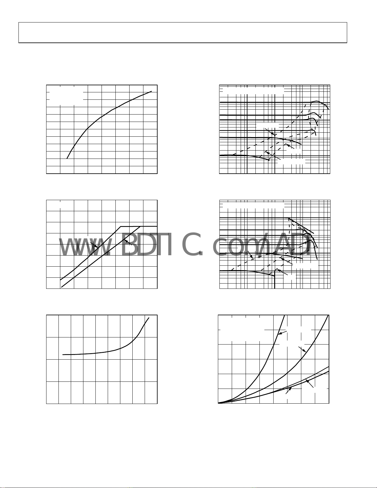
TYPICAL PERFORMANCE CHARACTERISTICS
TA = 25°C, ±VS = ±5 V (except AD737J-5, ±VS = ±2.5 V), CAV = 33 µF, CC = 10 µF, f = 1 kHz, sine wave input applied to Pin 2, unless
otherwise specified.
0.7
0.5
VIN = 200mV rms
C
= 100µF
AV
C
= 22µF
F
10
CAV = 22µF, CF = 4.7µF, CC = 22µF
1V
0.3
0.1
0
–0.1
–0.3
ADDITIONA L ERROR (% of Read ing)
–0.5
04286121410 16
SUPPLY VOLTAGE (±V)
Figure 5. Additional Error vs. Supply Voltage
16
DC COUPL ED
14
12
10
8
6
4
PEAK INPUT BEFO RE CLIPPI NG (V)
2
0
04286121410 16
PIN 1
PIN 2
SUPPLY VOLTAGE (±V)
Figure 6. Maximum Input Level vs. Supply Voltage
25
20
100mV
10mV
INPUT LEVEL (rms)
1mV
00828-005
100µV
0.1 1 10010 1000
1% ERROR
10% ERROR
FREQUENCY (kHz)
–3dB
00828-008
Figure 8. Frequency Response Driving Pin 1
10
CAV = 22µF, CF = 4.7µF, CC = 22µF
1V
100mV
10mV
INPUT LEVEL (rms)
1mV
00828-006
100µV
0.1 1 10010 1000
1% ERROR
FREQUENCY (kHz )
10% ERROR
–3dB
00828-009
Figure 9. Frequency Response Driving Pin 2
6
3ms BURST OF 1kHz =
3 CYCLES
200mV rms SIGNA L
5
= 22µF
C
C
= 100µF
C
F
4
CAV = 10µF
CAV = 33µF
15
SUPPLY CURRENT (µA)
10
5
0246 81012141618
DUAL SUPPLY VOLTAGE (±V)
Figure 7. Supply Current (Power-Down Mode) vs. Supply Voltage (Dual)
00828-007
3
2
1
ADDITIONAL ERRO R (% of Readi ng)
0
12345
CREST FACTOR (V
Figure 10. Additional Error vs. Crest Factor
Rev. G | Page 8 of 24
CAV = 250µF
/V rms)
PEAK
CAV = 100µF
00828-010

AD737
V
V
www.BDTIC.com/ADI
0.8
VIN = 200mV rms
C
= 100µF
AV
0.6
C
= 22µF
F
0.4
0.2
0
–0.2
–0.4
ADDITIONA L ERROR (% of Read ing)
–0.6
–0.8
–60 –20–40 200 60 80 100 12040 140
TEMPERATURE (°C)
Figure 11. Additional Error vs. Temperature
00828-011
1.0
0.5
0
–0.5
–1.0
ERROR (% of Read ing)
–1.5
–2.0
CAV = 22µF, CC = 47µF,
C
= 4.7µF
F
–2.5
10mV 100mV 1V 2V
INPUT LEVEL (rms)
Figure 14. Error vs. RMS Input Level Using Circuit of Figure 29
00828-014
500
400
300
200
DC SUPPLY CURRENT (µA)
100
0
0 0.2 0.4 0.6 0.8 1.0
RMS INPUT LEVEL (V)
Figure 12. DC Supply Current vs. RMS Input Level
10m
AC COUPL ED
1mV
100
10
AVERAGING CAPACITOR (µF)
00828-012
1
10 100 1k
–1%
FREQUENCY (Hz)
–0.5%
VIN = 200mV rms
C
= 47µF
C
C
= 47µF
F
00828-015
Figure 15. Value of Averaging Capacitor vs. Frequency
for Specif
ied Averaging Error
1
–1%
100mV
–0.5%
INPUT LEVEL (rms)
100µV
10µV
100 1k 10k 100k
–3dB FREQUENC Y (Hz)
Figure 13. RMS Input Level vs. –3 dB Frequency
00828-013
10mV
INPUT LEVEL (rms)
1mV
1 10 100 1k
Figure 16. RMS Input Level vs. Frequency for Specified Averaging Error
Rev. G | Page 9 of 24
FREQUENCY ( Hz)
AC COUPLED
C
= 10µF, CC = 47µF,
AV
C
= 47µF
F
00828-016

AD737
V
n
A
V
www.BDTIC.com/ADI
4.0
10
3.5
3.0
2.5
2.0
INPUT BIAS CURRENT (pA)
1.5
1.0
024 68 121410 16
SUPPLY VOLTAGE (±V)
Figure 17. Input Bias Current vs. Supply Voltage
1
100mV
CAV = 10µF
10mV
INPUT LEVEL (rms)
1mV
CAV = 33µF
CC = 22µF
C
= 0µF
F
CAV = 100µF
1nA
100pA
10pA
INPUT BIAS CURRENT
1pA
00828-017
100fA
–55 –35 –15 5 25 65 85 10545 125
TEMPERATURE (°C)
00828-019
Figure 19. Input Bias Current vs. Temperature
10
VS=±2.5V,
C
= 22µF, CF = 4.7µF, CC = 22µF
AV
1V
100mV
10mV
INPUT LEVEL (rms)
1mV
100µV
1ms 10ms 100ms 1s 10s 100s
SETTLING TIME
Figure 18. RMS Input Level vs. Settling Time for Three Values of C
00828-018
AV
100µV
0.1 1 10 100 1000
FREQUENCY ( kHz)
Figure 20. Frequency Response Driving Pin 1
00828-020
Rev. G | Page 10 of 24

AD737
V
www.BDTIC.com/ADI
10
100mV
VS=±2.5V,
C
= 22µF, CF = 4.7µF, CC = 22µF
AV
1V
1.0
0.5
0
–0.5
10mV
INPUT LEVEL (rms)
1mV
100µV
0.1 1 10 100 1000
0.5%
10%
–3dB
1%
FREQUENCY (kHz)
Figure 21. Error Contours Driving Pin 1
5
3 CYCLES OF 1kHz
200mV rms
V
= ±2.5V
S
4
C
= 22µF
C
C
= 100µF
F
3
2
1
ADDITIONA L ERROR (% of Read ing)
0
1234
CREST FACTOR
CAV =
22µF
CAV =
10µF
CAV =
100µF
Figure 22. Additional Error vs. Crest Factor for Various Values of C
CAV =
33µF
CAV =
220µF
00828-021
00828-022
5
AV
–1.0
ERROR (% of Read ing)
–1.5
–2.0
CAV = 22µF, VS = ±2.5V
C
= 47µF, CF = 4.7µF
C
–2.5
10mV 100mV 1V 2V
INPUT LEVEL (rms)
00828-023
Figure 23. Error vs. RMS Input Level Driving Pin 1
Rev. G | Page 11 of 24

AD737
www.BDTIC.com/ADI
THEORY OF OPERATION
As shown in Figure 24, the AD737 has four functional subsections: an input amplifier, a full-wave rectifier, an rms core, and a
bias section. The FET input amplifier allows a high impedance,
buffered input at Pin 2 or a low impedance, wide dynamic range
input at Pin 1. The high impedance input, with its low input bias
current, is ideal for use with high impedance input attenuators.
The input signal can be either dc coupled or ac coupled to the
input amplifier. Unlike other rms converters, the AD737 permits
both direct and indirect ac coupling of the inputs. AC coupling is
provided by placing a series capacitor between the input signal
and Pin 2 (or Pin 1) for direct coupling and between Pin 1 and
ground (while driving Pin 2) for indirect coupling.
AC
C
10µF
C =
+
DC
OPTIONAL RETURN PAT H
CURRENT
MODE
ABSOLUTE
VAL UE
C
V
V
IN
POWER
DOWN
–V
1
C
IN
2
3
S
4
8kΩ
FET
OP AMP
1
<10pA
B
BIAS
SECTION
RMS
TRANSLINEAR
CORE
POSITIVE SUPPLY
COMMON
NEGATI VE SUPPLY
C
33µF
8kΩ
A
+
0.1µF
0.1µF
8
COM
C
F
+
10µF
(OPTIONAL
+V
7
S
LPF)
6
OUTPUT
C
5
AV
+V
S
–V
S
Figure 24. AD737 True RMS Circuit (Test Circuit)
The output of the input amplifier drives a full-wave precision
rectifier, which, in turn, drives the rms core. It is the core that
provides the essential rms operations of squaring, averaging,
and square rooting, using an external averaging capacitor, C
Without C
, the rectified input signal passes through the core
AV
.
AV
unprocessed, as is done with the average responding connection
(see Figure 26). In the average responding mode, averaging is
ca
rried out by an RC post filter consisting of an 8 kΩ internal
scale factor resistor connected between Pin 6 and Pin 8 and an
external averaging capacitor, C
tional filtering stage reduces any output ripple that was not
removed by the averaging capacitor.
Finally, the bias subsection permits a power-down function.
educes the idle current of the AD737 from 160 µA to a
This r
mere 30 µA. This feature is selected by connecting Pin 3 to
Pin 7 (+V
).
S
TYPES OF AC MEASUREMENT
The AD737 is capable of measuring ac signals by operating as
either an average responding converter or a true rms-to-dc converter. As its name implies, an average responding converter
computes the average absolute value of an ac (or ac and dc)
voltage or current by full-wave rectifying and low-pass filtering
the input signal; this approximates the average. The resulting
output, a dc average level, is then scaled by adding (or reducing)
gain; this scale factor converts the dc average reading to an rms
equivalent value for the waveform being measured. For example,
the average absolute value of a sine wave voltage is 0.636 that of
V
; the corresponding rms value is 0.707 times V
PEAK
Therefore, for sine wave voltages, the required scale factor is
1.11 (0.707 divided by 0.636).
In contrast to measuring the average value, true rms measure-
ent is a universal language among waveforms, allowing the
m
magnitudes of all types of voltage (or current) waveforms to be
compared to one another and to dc. RMS is a direct measure of
the power or heating value of an ac voltage compared to that of
a dc voltage; an ac signal of 1 V rms produces the same amount
of heat in a resistor as a 1 V dc signal.
Mathematically, the rms value of a voltage is defined (using a
plified equation) as
sim
2
)( rms V
VAvg=
This involves squaring the signal, taking the average, and then
taining the square root. True rms converters are smart recti-
ob
fiers; they provide an accurate rms reading regardless of the
type of waveform being measured. However, average responding
00828-024
converters can exhibit very high errors when their input signals
deviate from their precalibrated waveform; the magnitude of
the error depends on the type of waveform being measured. As
an example, if an average responding converter is calibrated to
measure the rms value of sine wave voltages and then is used to
measure either symmetrical square waves or dc voltages, the
converter has a computational error 11% (of reading) higher
than the true rms value (see
The transfer function for the AD737 is
2
VAvg=
OUT
IN
. In the rms circuit, this addi-
F
Table 5 ).
)( V
PEAK
.
Rev. G | Page 12 of 24

AD737
www.BDTIC.com/ADI
DC ERROR, OUTPUT RIPPLE, AND AVERAGING ERROR
Figure 25 shows the typical output waveform of the AD737 with
a sine wave input voltage applied. As with all real-world devices,
the ideal output of V
the output contains both a dc and an ac error component.
E
O
Figure 25. Output Waveform for Sine Wave Input Voltage
As shown, the dc error is the difference between the average of
the output signal (when all the ripple in the output has been
removed by external filtering) and the ideal dc output. The dc
error component is, therefore, set solely by the value of the
averaging capacitor used—no amount of post filtering (using a
very large postfiltering capacitor, C
to equal its ideal value. The ac error component, an output
ripple, can be easily removed using a large enough C
In most cases, the combined magnitudes of the dc and ac error
mponents must be considered when selecting appropriate
co
values for C
and CF capacitors. This combined error, repre-
AV
senting the maximum uncertainty of the measurement, is
termed the averaging error and is equal to the peak value of the
output ripple plus the dc error. As the input frequency increases,
both error components decrease rapidly. If the input frequency
doubles, the dc error and ripple reduce to one-quarter and
one-half of their original values, respectively, and rapidly
become insignificant.
= VIN is never exactly achieved; instead,
OUT
IDEAL
E
O
DC ERROR = EO – EO (IDEAL)
DOUBLE-FREQUENCY
RIPPLE
AVERAGE E
) allows the output voltage
F
= E
O
O
TIME
.
F
00828-026
AC MEASUREMENT ACCURACY AND CREST FACTOR
The crest factor of the input waveform is often overlooked when
determining the accuracy of an ac measurement. Crest factor is
defined as the ratio of the peak signal amplitude to the rms
amplitude (crest factor = V
/V rms). Many common
PEAK
waveforms, such as sine and triangle waves, have relatively low
crest factors (≥2). Other waveforms, such as low duty cycle
pulse trains and SCR waveforms, have high crest factors. These
types of waveforms require a long averaging time constant to
average out the long time periods between pulses.
hows the additional error vs. the crest factor of the AD737 for
s
various values of C
.
AV
Figure 10
CALCULATING SETTLING TIME
Figure 18 can be used to closely approximate the time required
for the AD737 to settle when its input level is reduced in
amplitude. The net time required for the rms converter to settle
is the difference between two times extracted from the graph:
the initial time minus the final settling time. As an example,
consider the following conditions: a 33 µF averaging capacitor,
an initial rms input level of 100 mV, and a final (reduced) input
level of 1 mV. From
th
e 100 mV line intersects the 33 µF line) is approximately
80 ms. The settling time corresponding to the new or final input
level of 1 mV is approximately 8 seconds. Therefore, the net
time for the circuit to settle to its new value is 8 seconds minus
80 ms, which is 7.92 seconds.
Note, because of the smooth decay characteristic inherent with
a ca
pacitor/diode combination, this is the total settling time to
the final value (not the settling time to 1%, 0.1%, and so on, of
the final value). Also, this graph provides the worst-case settling
time, because the AD737 settles very quickly with increasing
input levels.
Figure 18, the initial settling time (where
Table 5. Error Introduced by an Average Respondi
Type of Waveform
1 V Peak Amplitude
Undistorted Sine Wave 1.414 0.707 0.707 0
Symmetrical Square Wave 1.00 1.00 1.11 11.0
Undistorted Triangle Wave 1.73 0.577 0.555 −3.8
Gaussian Noise (98% of
Peaks <1 V)
Rectangular 2 0.5 0.278 −44
Pulse Train 10 0.1 0.011 −89
SCR Waveforms
50% Duty Cycle 2 0.495 0.354 −28
25% Duty Cycle 4.7 0.212 0.150 −30
Crest Factor
/V rms)
(V
PEAK
3 0.333 0.295 −11.4
ng Circuit When Measuring Common Waveforms
True RM S
Va
lue (V)
Reading of an Average Responding Circuit Calibrated to
an RMS Sine Wave Value (V) Error (%)
Rev. G | Page 13 of 24

AD737
R
www.BDTIC.com/ADI
APPLICATIONS
RMS MEASUREMENT—CHOOSING OPTIMUM
VALUE FOR C
Because the external averaging capacitor, CAV, holds the rectified input signal during rms computation, its value directly
affects the accuracy of the rms measurement, especially at low
frequencies. Furthermore, because the averaging capacitor
appears across a diode in the rms core, the averaging time constant increases exponentially as the input signal is reduced. This
means that as the input level decreases, errors due to nonideal
averaging decrease, while the time it takes for the circuit to settle
to the new rms level increases. Therefore, lower input levels
allow the circuit to perform better (due to increased averaging)
but increase the waiting time between measurements. When
selecting C
settling time is required.
AV
AV
, a trade-off between computational accuracy and
RAPID SETTLING TIMES VIA THE AVERAGE RESPONDING CONNECTION
Because the average responding connection shown in Figure 26
does not use an averaging capacitor, its settling time does not vary
with input signal level; it is determined solely by the RC time
constant of C
C
V
IN
POWE
DOWN
and the internal 8 kΩ output scaling resistor.
F
8kΩ
1
C
2
3
–V
4
S
INPUT
AMPLIFI ER
BIAS
SECTION
POSITIVE SUPPLY
COMMON
NEGATIVE SUPPLY
Figure 26. AD737 Average Responding Circuit
AD737
FULL-WAVE
RECTIFI ER
RMS
CORE
8kΩ
0.1µF
0.1µF
8
COM
+V
7
S
6
OUTPUT
C
5
AV
+V
S
–V
S
+
C
F
33µF
V
OUT
00828-025
SELECTING PRACTICAL VALUES FOR CAPACITORS
Tabl e 6 provides practical values of CAV and CF for several
common applications.
The input coupling capacitor, C
internal input scaling resistor, determines the −3 dB low frequency
roll-off. This frequency, F
F
L
1
××π=80002
, in conjunction with the 8 kΩ
C
, is equal to
L
(
FaradsinC
C
(1)
)
Note that at F
(−3 dB) of reading. To reduce this error to 0.5% of reading,
choose a value of C
frequency to be measured.
In addition, if the input voltage has more than 100 mV of dc
o
ffset, the ac coupling network at Pin 2 is required in addition
to Capacitor C
SCALING INPUT AND OUTPUT VOLTAGES
The AD737 is an extremely flexible device. With minimal
external circuitry, it can be powered with single- or dualpolarity power supplies, and input and output voltages are
independently scaleable to accommodate nonmatching I/O
devices. This section describes a few such applications.
Extending or Scaling the Input Range
For low supply voltage applications, the maximum peak voltage
to the device is extended by simply applying the input voltage to
Pin 1 across the internal 8 kΩ input resistor. The AD737 input
circuit functions quasi differentially, with a high impedance,
FET input at Pin 2 (noninverting) and a low impedance input at
Pin 1 (inverting, see
s a voltage-to-current converter connected to the summing
a
node of a feedback loop around the input amplifier. Because the
feedback loop servos the summing node voltage to match the
voltage at Pin 2, the maximum peak input voltage increases
until the internal circuit runs out of headroom, approximately
double for a symmetrical dual supply.
Battery Operation
All the level-shifting for battery operation is provided by the
3½ digit converter, shown in Figure 27. Alternatively, an
ernal op amp adds flexibility by accommodating nonzero
ext
common-mode voltages and providing output scaling and
offset to zero. When an external operational amplifier is used,
the output polarity is positive going.
Figure 28 shows an op amp used in a single-supply application.
ote the combined input resistor value (R1 + R2 + 8 kΩ)
N
matches that of the Feedback Resistor R5. In this instance, the
magnitudes of the output dc voltage and the rms of the ac input
are equal. R3 and R4 provide current to offset the output to 0 V.
Scaling the Output Voltage
The output voltage may be scaled to the input rms voltage. For
e
xample, assume the AD737 is retrofitted to an existing application using an averaging responding circuit (full-wave rectifier).
The power supply is 12 V; the input voltage is 10 V ac, and the
desired output is 6 V dc.
, the amplitude error is approximately −30%
L
that sets FL at one-tenth of the lowest
C
.
C
Figure 26). The internal 8 kΩ resistor behaves
Rev. G | Page 14 of 24

AD737
www.BDTIC.com/ADI
For convenience, use the same combined input resistance as
shown in Figure 28. Calculate the rms input current as
= A 125
INMAG
Next, using the I
feedback resistor required for 6 V output using
R
FB
Select the closest-value standard 1% resistor, 47.5 kΩ.
Since the supply is 12 V, the common-mode voltage at the
divider R7/R8 is
(R3 + R4) is equal to the feedback resistor, or 47.5 kΩ.
Table 6. AD737 Capacitor Selection
Application RMS Input Level
General-Purpose RMS
Computation
200 Hz 5 15 1 36 ms
0 mV to 200 mV 20 Hz 5 33 10 360 ms
200 Hz 5 3.3 1 36 ms
General-Purpose Average
Responding
200 Hz None 3.3 120 ms
0 mV to 200 mV 20 Hz None 33 1.2 s
200 Hz None 3.3 120 ms
SCR Waveform
Measurement
60 Hz 5 82 27 1.0 s
0 mV to 100 mV 50 Hz 5 50 33 1.2 s
60 Hz 5 47 27 1.0 s
Audio Applications
Speech 0 mV to 200 mV 300 Hz 3 1.5 0.5 18 ms
Music 0 mV to 100 mV 20 Hz 10 100 68 2.4 s
1
Settling time is specified over the stated rms input level with the input signal increasing from zero. Settling times are greater for decreasing amplitude input signals.
OUTMAG
V 6
=
A 125
μ
6 V, and the combined resistor value
V 10
++
k 8 k 2.5 k 69.8
value from Equation 2, calculate the
k 48.1
=
(3)
0 V to 1 V 20 Hz 5 150 10 360 ms
0 V to 1 V 20 Hz None 33 1.2 s
0 mV to 200 mV 50 Hz 5 100 33 1.2 s
II =μ=
(2)
OUTMAG
Low Frequency
C
utoff (−3 dB)
R2 is used to calibrate the transfer function (gain), and R4 sets
t
he output voltage to zero with no input voltage.
Perform calibration as follows:
ith no ac input applied, adjust R4 for 0 V.
1. W
2. A
pply a known input to the input.
3. A
djust trimmer R2 until the input and output match.
The op amp selected for any single-supply application must be
a ra
il-to-rail type, for example an AD8541, shown in Figure 28.
F
or higher voltages, a higher voltage part, such as an OP196,
can be used. When calibrating to 0 V, the specified voltage
above ground for the operational amplifier must be taken into
account. Adjust R4 slightly higher as appropriate.
Maximum
Crest Factor C
(μF) CF (μF) Settling Time1 to 1%
AV
Rev. G | Page 15 of 24

AD737
V
T
R
www.BDTIC.com/ADI
IN
SWITCH CLO SED
ACTIVATES
POWER-DOWN
MODE. AD737 DR AW S
JUST 40µA IN THIS MODE
1PRV
0.01µF
9MΩ
900kΩ
90kΩ
10kΩ
200mV
2V
20V
200V
1µF
1N4148
47kΩ
1W
1N4148
+
POWER
DOWN
–V
C
10µF
C
V
IN
+
C
+
C
8kΩ
1
2
3
S
4
INPUT
AMPLIFIER
BIAS
SECTION
1µF
AD737
FULL-WAVE
RECTIFIER
RMS
CORE
8kΩ
AD589
COM
8
+V
S
7
OUTPUT
6
C
AV
5
+
1.23V
+V
33µF
20kΩ
200kΩ
50kΩ
1MΩ
0.1µF
+V
S
1
/2 DIGIT ICL7136
3
TYPE CONVERT ER
REF HIGH
REF LOW
COMMON
LOW
ANALOG
HIGH
–V
S
+
9V
00828-027
Figure 27. 3½ Digit DVM Circuit
INPUT SCALE FACTOR ADJ
R1
69.8kΩ
1%
R2
5kΩ
0.01µF
C
F
C
1
C
V
2
3
4
IN
POWER
DOWN
–V
S
AD737
C2
COM
+V
OUTPUT
C
8
NC
5V
7
S
OUTPUT ZERO
6
5
AV
R3
78.7kΩ
ADJUST
R4
5kΩ
C3
0.01µF
0.47µF
80.6kΩ
1
2
AD8541AR
3
4
R5
5V
0.01µF
7
6
5
OUTPUT
INPU
C1
0.47µF
NC = NO CONNECT
C
AV
33µF
+
C4
2.2µF
C5
1µF
R7
100kΩ
100kΩ
2.5V
R8
+
Figure 28. Battery-Powered Operation for 200 mV Maximum RMS Full-Scale Input
C
C
C
V
IN
POWE
DOWN
10µF
+
8kΩ
1
C
FULL-WAVE
2
AMPLIFIER
BIAS
3
SECTION
–V
S
4
INPUT
RECTIFIER
RMS
CORE
C
AV
33µF
+
100Ω
AD737
8kΩ
SCALE FACTOR
ADJUST
COM
8
200Ω
+V
7
S
10µF
OUTPUT
6
C
AV
5
+
C
F
V
OUT
00828-029
Figure 29. External Scale Factor Trim
5V
00828-028
Rev. G | Page 16 of 24

AD737
T
A
www.BDTIC.com/ADI
C
C
C
10µF
C
8kΩ
+
1
2
V
IN
POWER
3
DOWN
–V
S
4
NC = NO CONNECT
*Q1, Q2 PART OF RCA CA3046 OR SI MILAR NPN T RANSISTO R ARRAY.
**R1 + R
IN Ω = 10,000 ×
CAL
AMPLIFIER
BIAS
SECTION
R
CAL
INPUT
**
0dB INPUT LEVEL IN V
AD737
FULL-WAVE
RECTIFIE R
RMS
CORE
+
C
AV
R1**
4.3V
COM
8kΩ
8
NC
+V
7
S
OUTPUT
6
C
AV
5
I
REF
Figure 30. dB Output Connection
OFFSET
DJUST
+V
S
500kΩ
1MΩ
1kΩ
–V
S
14
13
Q1
12
*
2
3
10
3500PPM/°C
60.4Ω
SCALE
FAC TOR
TRIM
AD711
*
11
Q2
9
1kΩ
PRECISION
RESISTOR
TYPE PT/ST
6
CORP
2kΩ
31.6kΩ
dB OUTPU
100mV/dB
00828-030
V
IN
POWER
DOWN
C
C
8kΩ
1
2
3
INPUT
AMPLIFIER
FULL-WAVE
RECTIFIER
AD737
COM
8
7
6
499Ω
1kΩ
SCALE
FACT OR
+V
ADJUST
S
V
OUT
00828-031
Figure 31. DC-Coupled Offset Voltage and Scale Factor Trims
Rev. G | Page 17 of 24

AD737
www.BDTIC.com/ADI
AD737 EVALUATION BOARD
An evaluation board, AD737-EVALZ, is available for experimenting or becoming familiar with rms-to-dc converters.
Figure 32 is a photograph of the board; Figure 34 to Figure 37
s
how the signal and power plane copper patterns. The board is
designed for multipurpose applications and can be used for the
AD736 as well. Although not shipped with the board, an optional
socket that accepts the 8lead surface mount package is
available from Enplas Corp.
Figure 32. AD737 Evaluation Board
Figure 35. AD737 Evaluation B
00828-038
oard—Secondary-Side Copper
00828-034
Figure 33. AD737 Evaluation Board—Component-Side Silkscreen
As described in the Applications section, the AD737 may be connected in a variety of ways. As shipped, the board is configured for
dual supplies with the high impedance input connected and the
power-down feature disabled. Jumpers are provided for connecting
the input to the low impedance input (Pin 1) and for dc connections to either input. The schematic with movable jumpers is
shown in
ne
board is tested prior to shipment and only requires a power supply
connection and a precision meter, to perform measurements.
Tabl e 7 provides a bill of materials for the AD737 evaluation board.
Figure 38. The jumper positions in black are default con-
ctions; the dotted-outline jumpers are optional connections. The
00828-035
Figure 36. AD737 Evaluation Board—Internal Power Plane
00828-032
00828-036
Figure 37. AD737 Evaluation Board—Internal Ground Plane
Figure 34. AD737 Evaluation B
oard—Component-Side Copper
00828-033
Rev. G | Page 18 of 24

AD737
–V
V
www.BDTIC.com/ADI
J1
GND1 GND3GND2 GND4
W1
DC
COUP
V
IN
C
IN
0.1µF
GND
P2
HI-Z SEL
IN
R1
1MΩ
FILT
NORM
W4
LO-Z IN
W2
PD
SEL
PIN3
C1
+
10µF
25V
LO-Z
HI-Z
1
C
2
V
3
POWER
DOWN
4
–V
+
V
S
J3
–V
C4
0.1µF
Figure 38. AD737 Evaluation Board Schematic
Table 7. AD737 Evaluation Board Bill of Materials
Qty Name Description Reference Designator Manufacturer Mfg. Part Number
1 Test Loop Red +VS Components Corp. TP-104-01-02
1 Test Loop Green −VS Components Corp. TP-104-01-05
2 Capacitor Tantalum 10 μF, 25 V C1, C2 Nichicon F931E106MCC
3 Capacitor 0.1 μF, 16 V, 0603, X7R C4, C6, CIN KEMET C0603C104K4RACTU
1 Capacitor Tantalum 33 μF, 16V, 20%, 6032 CAV Nichicon F931C336MCC
5 Test Loop Purple CAV, HI-Z, LO-Z, VIN, V
1 Integrated Circuit RMS-to-DC converter DUT Analog Devices, Inc. AD737JRZ
4 Test Loop Black GND1, GND2, GND3, GND4 Components Corp. TP-104-01-00
2 Connector BNC, right angle J1, J2 AMP 227161-1
1 Header 6 Pins, 2 × 3 J3 3M 929836-09-03
1 Header 3 Pins P2 Molex 22-10-2031
1 Resistor 1 MΩ, 1/10 W, 1%, 0603 R1 Panasonic ERJ3EKF1004V
2 Resistor 0 Ω, 5%, 0603 R3, R4 Panasonic ERJ3GEY0R00V
4 Header 2 Pins, 0.1" center W1, W2, W3, W4 Molex 22-10-2021
S
–VS+V
W3
AC COUP
+
CC
DUT
AD737
C
IN
S
C
33µF
S
16V
C
+
S
S
COM
+V
OUTPUT
C
AV
+
F2
C2
+
10µF
25V
R3
0Ω
R4
0Ω
8
7
S
C6
0.1µF
6
5
AV
Components Corp. TP-104-01-07
OUT
+V
CAV
V
OUT
S
J2
C
F1
00828-037
Rev. G | Page 19 of 24

AD737
www.BDTIC.com/ADI
OUTLINE DIMENSIONS
5.00 (0.1968)
4.80 (0.1890)
4.00 (0.1574)
3.80 (0.1497)
0.25 (0.0 098)
0.10 (0.0 040)
COPLANARI TY
0.10
CONTROL LING DI MENSIO NS ARE IN MILLI METERS; INCH DIMENS IONS
(IN PARENTHESES) ARE ROUNDED-O FF MIL LIME TER EQUIVALENTS F OR
REFERENCE O NLY AND ARE NOT APPROPRIATE FO R USE IN DESI GN.
85
1
1.27 (0.050 0)
SEATING
PLANE
COMPLI ANT TO JEDEC STANDARDS MS -012-A A
BSC
6.20 (0.2 440)
5.80 (0.2 284)
4
1.75 (0.0 688)
1.35 (0.0 532)
0.51 (0.0201)
0.31 (0.0122)
8°
0°
0.25 (0.0098)
0.17 (0.0067)
Figure 39. 8-Lead Standard Small Outline Package [SOIC_N]
Nar
row Body
(R-8)
Dimensions shown in millimeters and (inches)
0.50 (0.0196)
0.25 (0.0099)
1.27 (0.0500)
0.40 (0.0157)
45°
0.005 (0.13)
0.200 (5.08)
MAX
0.200 (5.08)
0.125 (3.18)
0.023 (0.58)
0.014 (0.36)
CONTROLLING DIMENSIONS ARE IN INCHES; MILLIMETER DIMENSIONS
(IN PARENTHESES) ARE ROUNDED-OFF INCH EQUIVALENTS FOR
060506-A
REFERENCE ONLY AND ARE NOT APPROPRIATE FOR USE IN DESIGN.
Figure 40. 8-Lead Ceramic Dual In-Line Package [CERDIP]
Dimensions shown in inches and (millimeters)
0.055 (1.40)
MIN
14
0.100 (2.54) BSC
0.405 (10.29) MAX
MAX
0.070 (1.78)
0.030 (0.76)
58
0.310 (7.87)
0.220 (5.59)
0.060 (1.52)
0.015 (0.38)
0.150 (3.81)
MIN
SEATING
PLANE
-8)
(Q
0.320 (8.13)
0.290 (7.37)
15°
0°
0.015 (0.38)
0.008 (0.20)
0.210 (5.33)
0.150 (3.81)
0.130 (3.30)
0.115 (2.92)
0.022 (0.56)
0.018 (0.46)
0.014 (0.36)
0.400 (10.16)
0.365 (9.27)
0.355 (9.02)
8
1
0.100 (2.54)
MAX
0.070 (1.78)
0.060 (1.52)
0.045 (1.14)
CONTROLL ING DIMENS IONS ARE IN INCHES; MILLIMETER DI MENSIONS
(IN PARENTHESES) ARE ROUNDED-OF F INCH EQUIVALENTS FOR
REFERENCE ONLY AND ARE NOT APPROPRI ATE FOR USE IN DES IGN.
CORNER LEADS MAY BE CONFIGURED AS WHOL E OR HALF LEADS.
5
0.280 (7.11)
0.250 (6.35)
0.240 (6.10)
4
BSC
0.015
(0.38)
MIN
SEATING
PLANE
0.005 (0.13)
MIN
COMPLIANT TO JEDEC STANDARDS MS-001
0.060 (1.52)
MAX
0.015 (0.38)
GAUGE
PLANE
0.325 (8.26)
0.310 (7.87)
0.300 (7.62)
0.430 (10.92)
MAX
Figure 41. 8-Lead Plastic Dual-In-Line Package [PDIP]
(N-8)
Dim
ensions shown in inches and (millimeters)
0.195 (4.95)
0.130 (3.30)
0.115 (2.92)
0.014 (0.36)
0.010 (0.25)
0.008 (0.20)
070606-A
Rev. G | Page 20 of 24

AD737
www.BDTIC.com/ADI
ORDERING GUIDE
Model Temperature Range Package Description Package Option
AD737AN −40°C to +85°C 8-Lead Plastic Dual In-Line Package [PDIP] N-8
AD737ANZ
AD737AQ −40°C to +85°C 8-Lead Ceramic Dual In-Line Package [CERDIP] Q-8
AD737AR −40°C to +85°C 8-Lead Standard Small Outline Package [SOIC_N] R-8
AD737ARZ
AD737BQ −40°C to +85°C 8-Lead Ceramic Dual In-Line Package [CERDIP] Q-8
AD737JN 0°C to 70°C 8-Lead Plastic Dual In-Line Package [PDIP] N-8
AD737JNZ
AD737JR 0°C to 70°C 8-Lead Standard Small Outline Package [SOIC_N] R-8
AD737JR-REEL 0°C to 70°C 8-Lead Standard Small Outline Package [SOIC_N] R-8
AD737JR-REEL7 0°C to 70°C 8-Lead Standard Small Outline Package [SOIC_N] R-8
AD737JR-5 0°C to 70°C 8-Lead Standard Small Outline Package [SOIC_N] R-8
AD737JR-5-REEL 0°C to 70°C 8-Lead Standard Small Outline Package [SOIC_N] R-8
AD737JR-5-REEL7 0°C to 70°C 8-Lead Standard Small Outline Package [SOIC_N] R-8
AD737JRZ
AD737JRZ-R7
AD737JRZ-RL
AD737JRZ-5
AD737JRZ-5-R7
AD737JRZ-5-RL
AD737KN 0°C to 70°C 8-Lead Plastic Dual In-Line Package [PDIP] N-8
AD737KNZ
AD737KR 0°C to 70°C 8-Lead Standard Small Outline Package [SOIC_N] R-8
AD737KR-REEL 0°C to 70°C 8-Lead Standard Small Outline Package [SOIC_N] R-8
AD737KR-REEL7 0°C to 70°C 8-Lead Standard Small Outline Package [SOIC_N] R-8
AD737KRZ
AD737KRZ-RL
AD737KRZ-R7
AD737-EVALZ
1
Z = Pb-free part.
1
1
1
1
1
1
1
1
1
1
1
1
−40°C to +85°C 8-Lead Plastic Dual In-Line Package [PDIP] N-8
−40°C to +85°C 8-Lead Standard Small Outline Package [SOIC_N] R-8
0°C to 70°C 8-Lead Plastic Dual In-Line Package [PDIP] N-8
0°C to 70°C 8-Lead Standard Small Outline Package [SOIC_N] R-8
0°C to 70°C 8-Lead Standard Small Outline Package [SOIC_N] R-8
0°C to 70°C 8-Lead Standard Small Outline Package [SOIC_N] R-8
0°C to 70°C 8-Lead Standard Small Outline Package [SOIC_N] R-8
1
0°C to 70°C 8-Lead Standard Small Outline Package [SOIC_N] R-8
1
0°C to 70°C 8-Lead Standard Small Outline Package [SOIC_N] R-8
0°C to 70°C 8-Lead Plastic Dual In-Line Package [PDIP] N-8
0°C to 70°C 8-Lead Standard Small Outline Package [SOIC_N] R-8
0°C to 70°C 8-Lead Standard Small Outline Package [SOIC_N] R-8
0°C to 70°C 8-Lead Standard Small Outline Package [SOIC_N] R-8
Evaluation Board
Rev. G | Page 21 of 24

AD737
www.BDTIC.com/ADI
NOTES
Rev. G | Page 22 of 24

AD737
www.BDTIC.com/ADI
NOTES
Rev. G | Page 23 of 24

AD737
www.BDTIC.com/ADI
NOTES
©2006 Analog Devices, Inc. All rights reserved. Trademarks and
registered trademarks are the property of their respective owners.
C00828-0-12/06(G)
Rev. G | Page 24 of 24
 Loading...