

Differential Input,Dual,Simultaneous
V
V
V
V
www.BDTIC.com/ADI
Sampling, 4.25 MSPS, 14-Bit, SAR ADC
Preliminary Technical Data
FEATURES
Dual 14-bit SAR ADC
Simultaneous Sampling
Throughput rate: 4.25 MSPS Per Channel
Specified for V
Power dissipation:
35 mW at 4.25 MSPS
On-chip reference:
2.048 V ± 0.5% max @ 25°C, 10ppm/°C
Dual conversion with read
High speed serial interface:
SPI®-/QSPI™-/MICROWIRE™-/DSP-compatible
−40°C to +125°C operation
Shutdown mode: 10 µA max
16-lead TSSOP package
GENERAL DESCRIPTION
The AD73571 is a dual, 14-bit, high speed, low power, successive
approximation ADC that operates from a single 2.5 V power supply
and features throughput rates up to 4.25 MSPS. The part contains
two ADCs, each preceded by a low noise, wide bandwidth trackand-hold circuit that can handle input frequencies in excess of
200 MHz.
The conversion process and data acquisition use standard control
inputs allowing for easy interfacing to microprocessors or DSPs.
The input signal is sampled on the falling edge of
also initiated at this point. The conversion time is determined by
the SCLK frequency.
The AD7357 uses advanced design techniques to achieve very low
power dissipation at high throughput rates. With 2.5 V supply and
a 4.25 MSPS throughput rate, the part consumes 14 mA typically.
The part also offers flexible power/throughput rate management
when operating in normal mode as the quiescent current
consumption is so low.
The analog input range for the part is the differential common
mode +/- Vref/2. The AD7357 has an on-chip 2.048 V reference
that can be overdriven when an external reference is preferred.
The AD7357 is available in a 16-lead thin shrink small outline
package (TSSOP).
of 2.5 V
DD
CS
; conversion is
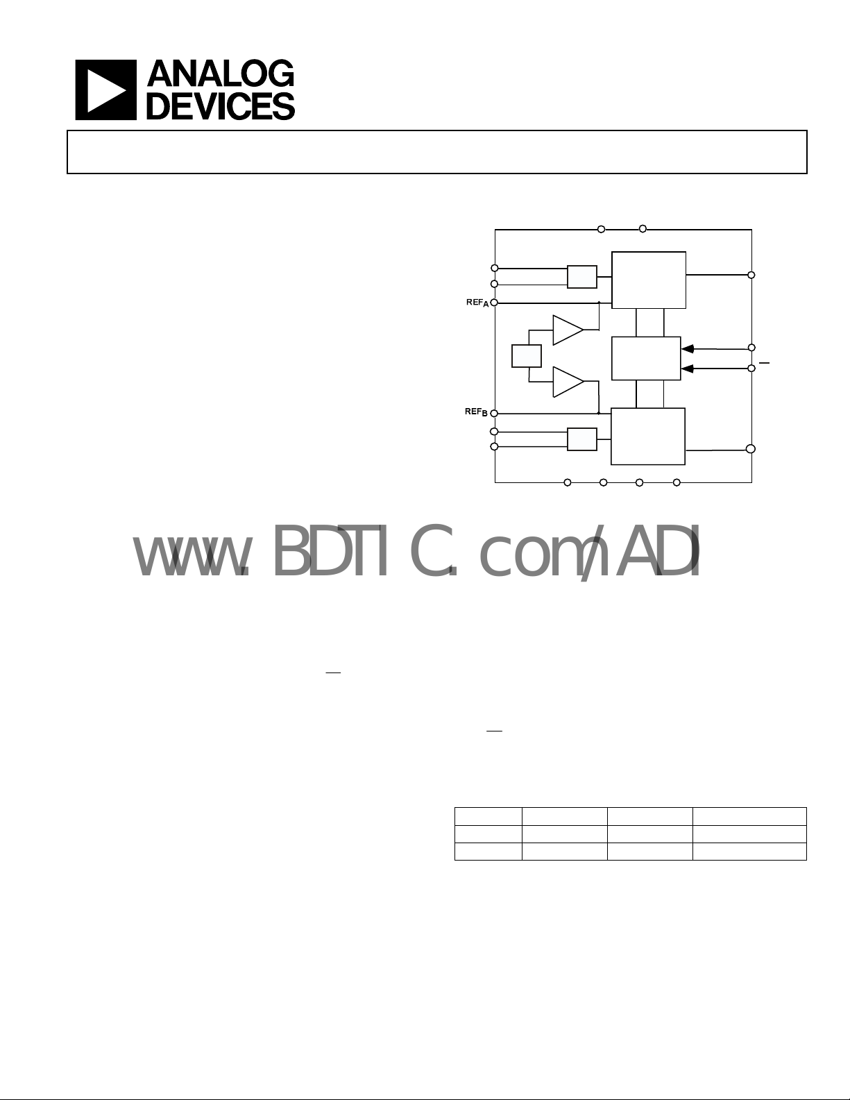
AD7357
FUNCTIONAL BLOCK DIAGRAM
Vdd
IN
A+
IN
A-
REF
IN
B+
V
IN
B-
BUF
BUF
AGND
T/H
T/H
AGND
PRODUCT HIGHLIGHTS
1. Two Complete ADC Functions Allow Simultaneous Sampling
and Conversion of Two Channels.
The conversion result of both channels is simultaneously
available on separate data lines or in succession on one data
line if only one serial port is available.
2. High Throughput with Low Power Consumption.
The AD7357 offers a 4.25 MSPS throughput rate with 35 mW
power consumption.
3.
The part features two standard successive approximation
ADCs with accurate control of the sampling instant via a
CS
input and once off conversion control.
1
Protected by U.S. Patent No. 6,681,332
Table 1: Related Devices.
Generic Resolution Throughput Analog Input
AD7356 12 5MSPS Differential
AD7352 12 3MSPS Differential
drive
14-BIT
SUCCESSIVE
APPROXIMATION
ADC
CONTROL
LOGIC
14-BIT
SUCCESSIVE
APPROXIMATION
ADC
REFGND
Figure 1.
DGND
AD7357
SDATA
SCLK
CS
SDATA
A
B
Rev. PrD
Information furnished by Analog Devices is believed to be accurate and reliable. However, no
responsibility is assumed by Anal og Devices for its use, nor for any infringements of p atents or other
rights of third parties that may result from its use. Specifications subject to change without notice. No
license is granted by implication or otherwise under any patent or patent rights of Analog Devices.
Trademarks and registered trademarks are the property of their respective owners.
One Technology Way, P.O. Box 9106, Norwood, MA 02062-9106, U.S.A.
Tel: 781.329.4700 www.analog.com
Fax: 781.461.3113 ©2007 Analog Devices, Inc. All rights reserved.

AD7357 Preliminary Technical Data
www.BDTIC.com/ADI
TABLE OF CONTENTS
Revision Historyx ............................................................................. 2
ADC Transfer Function............................................................. 11
Specifications..................................................................................... 3
AD7357 Specifications................................................................. 3
Timing Specifications .................................................................. 5
Absolute Maximum Ratings............................................................ 6
ESD Caution.................................................................................. 6
Pin Configuration and Function Descriptions............................. 7
Typical Performance Characteristics ............................................. 8
Terminology ...................................................................................... 9
Theory of Operation ...................................................................... 11
Circuit Information.................................................................... 11
Converter Operation.................................................................. 11
REVISION HISTORYX
09/07—Revision PrD
Analog Input Structure.............................................................. 11
Analog Inputs ............................................................................. 12
Modes of Operation ....................................................................... 13
Normal Mode.............................................................................. 13
Partial Power-Down Mode ....................................................... 13
Full Power-Down Mode............................................................ 13
Power-Up Times......................................................................... 15
Serial Interface ................................................................................ 16
Outline Dimensions....................................................................... 17
Ordering Guide............................................................................... 17
Rev. PrD | Page 2 of 17
Preliminary Technical Data AD7357
www.BDTIC.com/ADI
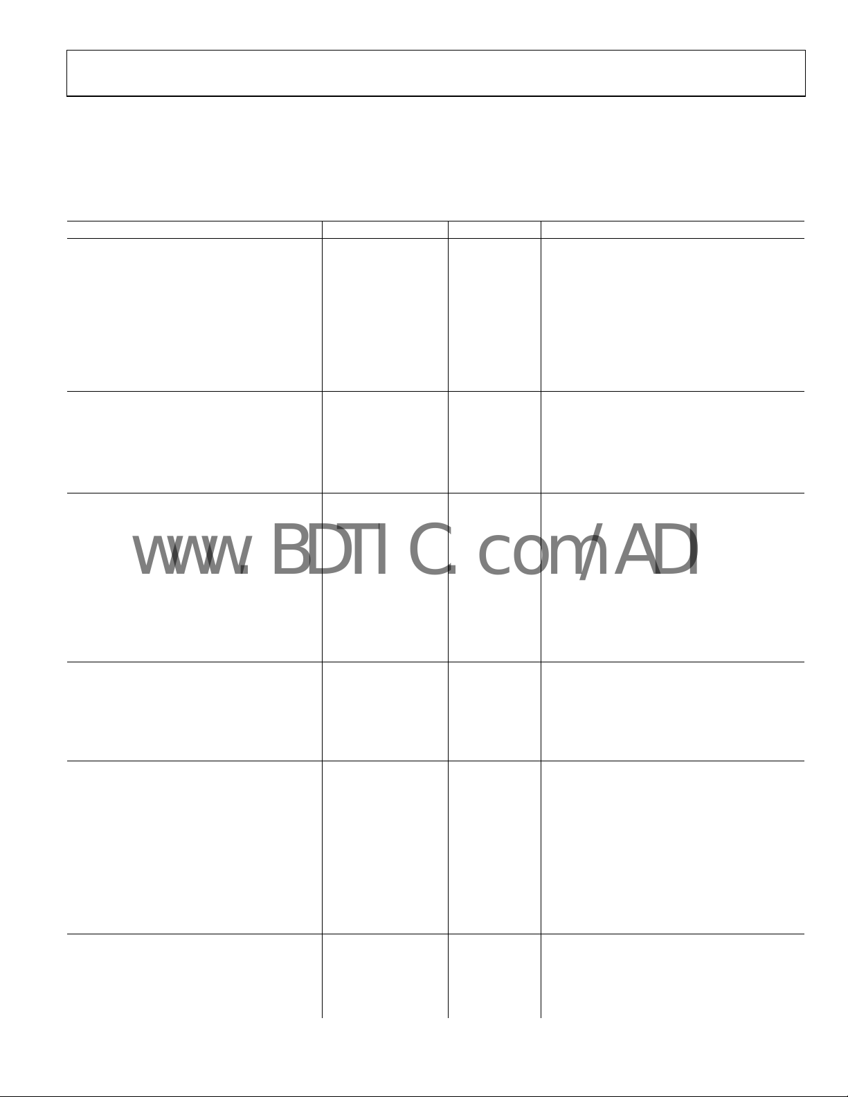
SPECIFICATIONS
AD7357 SPECIFICATIONS
VDD = 2.5 +/-10% V, V
T
= T
MIN
to T
A
1
, unless otherwise noted.
MAX
Table 1.
Parameter Specification Unit Test Conditions/Comments
DYNAMIC PERFORMANCE fIN = 1 MHz sine wave
Signal-to-Noise Ratio (SNR) 78 dB min
Signal-to-Noise and Distortion (SINAD) 77 dB min
Total Harmonic Distortion (THD) TBD
Spurious Free Dynamic Range (SFDR) TBD dB max
Intermodulation Distortion (IMD) fa = TBD Hz, fb = TBD Hz
Second Order Terms TBD dB typ
Third Order Terms TBD dB typ
Channel-to-Channel Isolation −85 dB typ f
SAMPLE AND HOLD
Aperture Delay 5 ns max
Aperture Delay Matching 40 ps max
Aperture Jitter 15 ps typ
Full Power Bandwidth 200 MHz typ @ 3 dB
30 MHz typ @ 0.1 dB
DC ACCURACY
Resolution 14 Bits
Integral Nonlinearity ±2 LSB max
Differential Nonlinearity ±0.99 LSB max Guaranteed no missed codes to 14 bits
Offset Error ±10 LSB max
Offset Error Match ±1 LSB typ
±6 LSB max
Gain Error ±10 LSB max
Gain Error Match ±1 LSB typ
±6 LSB max
ANALOG INPUT
Fully Differential Input Range: V
DC Leakage Current ±1 µA max
Input Capacitance 35 pF typ When in track
10 pF typ When in hold
REFERENCE INPUT/OUTPUT
V
Input Voltage Range 2.048+100mV / Vdd V min / V max
REF
DC Leakage Current ±1 µA max
V
Output Voltage 2.048 V ±0.5% max @ 25°C
REF
V
Temperature Coefficient 10 ppm⁄°C typ
REF
V
Long Term Stability 100 ppm typ For 1000 hours
REF
V
Output Voltage Hysteresis2 50 ppm typ
REF
V
Noise TBD
REF
V
Output Impedance TBD
REF
V
Input Capacitance TBD pF typ When in track
REF
LOGIC INPUTS
Input High Voltage, V
Input Low Voltage, V
Input Current, IIN ±1 µA max VIN = 0 V or V
Input Capacitance, CIN 10 pF typ
= 2.5 V to 3.3 +10% V, internal V
DRIVE
in+
and V
VCM ± V
in−
= 2.048 V, unless otherwise noted, F
REF
dB max
⁄2 V
REF
µV Typ
Ω Typ
0.6 × Vdrive V min
INH
0.3 × Vdrive V max
INL
= 80 MHz, F
CLKIN
= TBD kHz, f
IN
= common-mode voltage , V
V
CM
remain within GND⁄V
NOISE
= TBD kHz
DD
DRIVE
= 4.25 MSPS;
SAMPLE
in+
and V
in−
must
Rev. PrD | Page 3 of 17
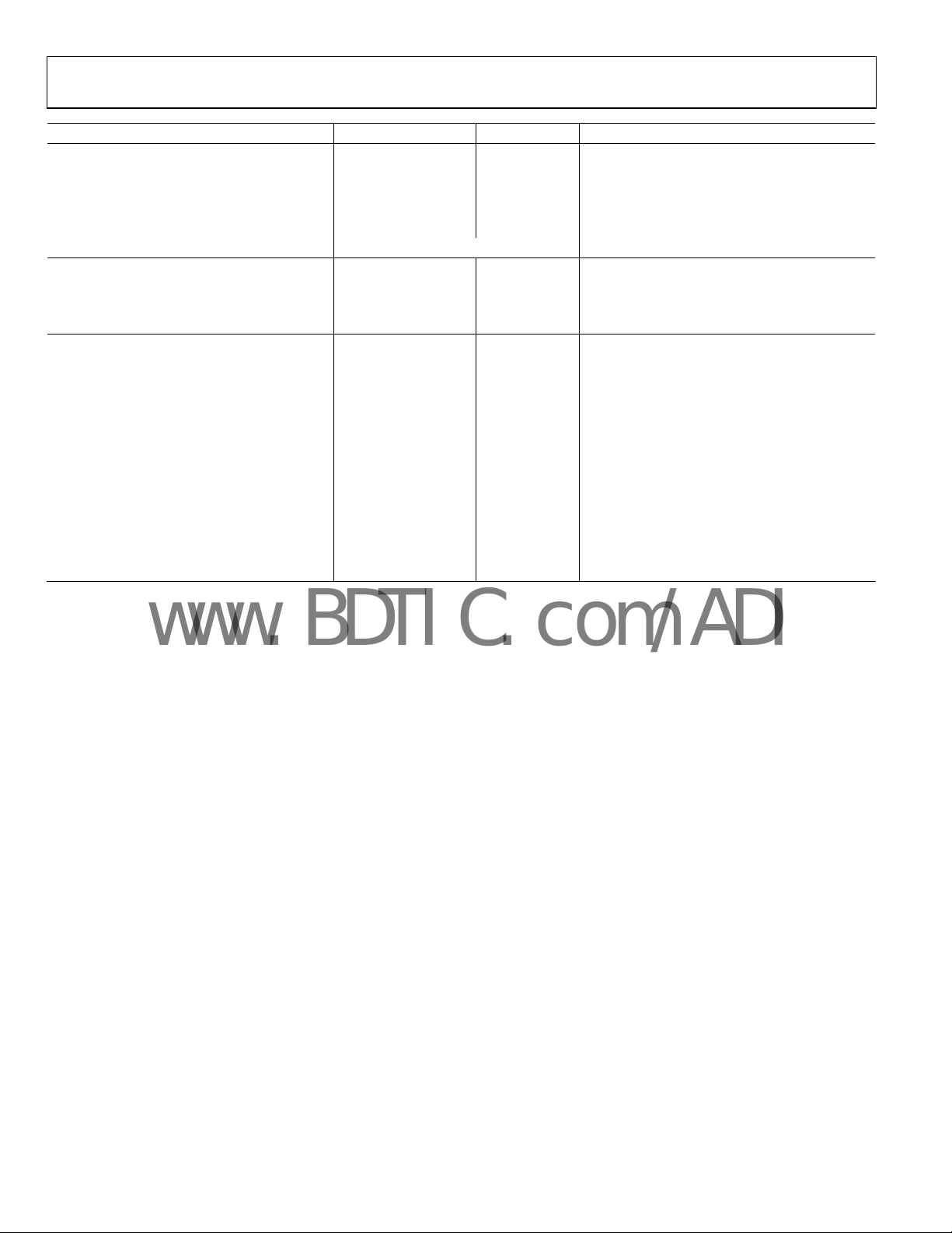
AD7357 Preliminary Technical Data
www.BDTIC.com/ADI
Parameter Specification Unit Test Conditions/Comments
LOGIC OUTPUTS
Output High Voltage, VOH Vdrive-0.2 V min
Output Low Voltage, VOL 0.2 V max
Floating-State Leakage Current ±1 µA max
Floating-State Output Capacitance TBD pF typ
Output Coding Straight Binary
CONVERSION RATE
Conversion Time t2 + 15.5 × t
Track-and-Hold Acquisition Time 30 ns max Full-scale step input
Throughput Rate 4.25 MSPS max
POWER REQUIREMENTS
VDD 2.5 V
V
2.5/3.3 V min/max
DRIVE
IDD Digital I⁄PS = 0 V or V
Normal Mode (Operational) 14 mA typ
Normal Mode (Static) 7 mA typ SCLK off
Partial Power-Down Mode 5 mA typ
Full Power-Down Mode 10 µA typ SCLK on or off
Power Dissipation
Normal Mode (Operational) 35 mW typ
Normal Mode (Static) 17.5 mW typ SCLK off
Partial Power-Down Mode 12.5 mW typ
Full Power-Down Mode 2.5 µW typ SCLK on or off
1
Temperature ranges are as follows: Y Grade: −40°C to +125°C, B Grade: −40°C to +85°C.
2
See theTerminology section.
ns
SCLK
DRIVE
Rev. PrD | Page 4 of 17
Preliminary Technical Data AD7357
www.BDTIC.com/ADI
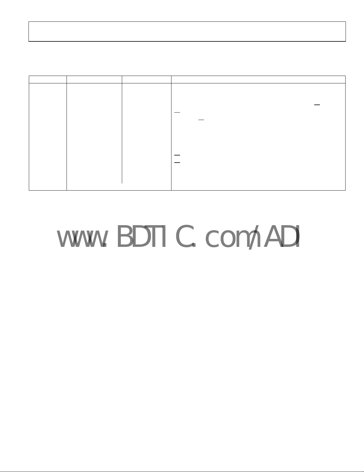
TIMING SPECIFICATIONS
VDD = 2.5 +/-10%V, V
= 2.5 V to 3.3 +10% V, internal reference = 2.048 V, TA = T
DRIVE
Table 2.
Parameter Limit at T
f
SCLK
50 kHz min
80 MHz max
t
CONVERT
t
5 ns min
QUIET
t
2
t
3
t
42
t2 +15.5 × t
5 ns min
TBD ns max
TBD ns max Data access time after SCLK falling edge
t5 0.40 t
t6 0.40 t
t
7
t
8
TBD ns min SCLK to data valid hold time
TBD ns max
t9 TBD ns min
t
10
TBD ns min SCLK falling edge to D
TBD ns max SCLK falling edge to D
Latency 1 Conversion Latency
1
Temperature ranges are as follows: Y Grade: −40°C to +125°C, B Grade: −40°C to +85°C.
2
The time required for the output to cross 0.4 V or 2.4 V.
, T
MIN
MAX
ns max 14 bit resolution, t
SCLK
Unit Description
Minimum time between end of serial read and next falling edge of
CS
to SCLK setup time
Delay from
SCLK
ns min SCLK high pulse width
SCLK
ns min SCLK low pulse width
CS
rising edge to D
CS
rising edge to falling edge pulse width
CS
until D
SCLK
OUT
MAX
= 1/f
A and D
OUT
A, D
OUT
OUT
SCLK
OUT
A, D
A, D
1
to T
, unless otherwise noted.
MIN
B are three-state disabled
OUT
B, high impedance
B, high impedance
OUT
B, high impedance
OUT
CS
Rev. PrD | Page 5 of 17
AD7357 Preliminary Technical Data
www.BDTIC.com/ADI
ABSOLUTE MAXIMUM RATINGS
Table 3.
Parameter Rating
VDD to AGND, DGND, REFGND
V
to AGND, DGND, REFGND −0.3 V to +3.8V
DRIVE
VDD to V
+2.8V to −3.8V
DRIVE
AGND to DGND to REFGND
Analog Input Voltages1 to AGND
Digital Input Voltages2 to DGND −0.3V to V
Digital Output Voltages3 to DGND
Input Current to Any Pin Except
Supplies
4
−0.3 V to +2.8V
−0.3 V to +0.3 V
−0.3 V to V
−0.3 V to V
+ 0.3 V
DD
DRIVE
DRIVE
+ 0.3V
±10 mA
+ 0.3 V
Operating Temperature Range
Y Grade
B Grade
Storage Temperature Range
−40°C to +125°C
−40°C to +85°C
−65°C to +150°C
Junction Temperature 150°C
TSSOP Package
θJA Thermal Impedance 143°C/W
θJC Thermal Impedance 45°C/W
Lead Temperature, Soldering
Reflow Temperature (10 to 30 sec) 255°C
ESD TBD kV
1
Analog input voltages are V
2
Digital input voltages are CS and SCLK.
3
Digital output voltages are SDATAA and SDATAB.
4
Transient currents of up to 100 mA will not cause SCR latch up.
INA+
, V
, V
, V
INB+
INB-
, REFA and REFB.
INA-
Stresses above those listed under Absolute Maximum Ratings
may cause permanent damage to the device. This is a stress
rating only; functional operation of the device at these or any
other conditions above those indicated in the operational
section of this specification is not implied. Exposure to absolute
maximum rating conditions for extended periods may affect
device reliability.
ESD CAUTION
ESD (electrostatic discharge) sensitive device. Electrostatic charges as high as 4000 V readily accumulate
on the human body and test equipment and can discharge without detection. Although this product
features proprietary ESD protection circuitry, permanent damage may occur on devices subjected to
high energy electrostatic discharges. Therefore, proper ESD precautions are recommended to avoid
performance degradation or loss of functionality.
Rev. PrD | Page 6 of 17

Preliminary Technical Data AD7357
www.BDTIC.com/ADI
PIN CONFIGURATION AND FUNCTION DESCRIPTIONS
Table 4. Pin Function Descriptions
Pin No. Mnemonic Description
9 VDD
Power Supply Input. The V
with a 0.1 µF capacitor and a 10 µF tantalum capacitor.
16 V
DRIVE
Logic Power Supply Input. The voltage supplied at this pin determines at what voltage the interface will
operate. This pin should be decoupled to DGND. The voltage at this pin may be different to that at V
10
Chip Select. Active low logic input. This input provides the dual function of initiating conversions on the
CS
AD7357 and framing the serial data transfer.
15
SCLK
Serial Clock. Logic input. A serial clock input provides the SCLK for accessing the data from the AD7357. This
clock is also used as the clock source for the conversion process.
SDATA
,
14,13
SDATA
A
B
Serial Data Outputs. The data output is supplied to each pin as a serial data stream. The bits are clocked out on
the falling edge of the SCLK input. 16 SCLK falling edges are required to access the 14 bits of data from the
AD7357. The data simultaneously appears on both data output pins from the simultaneous conversions of
both ADCs. The data stream consists of one leading zero followed by the 14 bits of conversion data followed by
a trailing zero. The data is provided MSB first. If CS is held low for 18 SCLK cycles rather than 16, then two
further trailing zeros will appear after the 14 bits of data. If CS is held low for a further 18 SCLK cycles on either
SDATA
or SDATAB , the data from the other ADC follows on the SDATA pin. This allows data from a
A
simultaneous conversion on both ADCs to be gathered in serial format on either SDATA
12 DGND
Digital Ground. This is the ground reference point for all digital circuitry on the AD7357. This pin should
connect to the DGND plane of a system. The DGND and AGND voltages should ideally be at the same potential
and must not be more than 0.3 V apart, even on a transient basis.
5, 11 AGND
Analog Ground. This is the ground reference point for all analog circuitry on the AD7357. All analog input
signals and should be referred to this AGND voltage. The AGND and DGND voltages should ideally be at the
same potential and must not be more than 0.3 V apart, even on a transient basis.
4 REFGND
Reference Ground. This is the ground reference point for the reference circuitry on the AD7357. Any external
reference signal should be referred to this REFGND voltage. Decoupling capacitors must be placed between
this pin and the REF
3, 6 REFA, REFB
Reference decoupling capacitor pins. Decoupling capacitors are connected between these pins and the
REFGND pin to decouple the reference buffer for each respective ADC. It is recommended to decouple the each
reference pin with a 10µF capacitor. Provided the output is buffered, the on-chip reference can be taken from
these pins and applied externally to the rest of the system. The nominal internal reference voltage is 2.048V
and this appears at these pins. These pins can also be overdriven by an external reference. The input voltage
range for the external reference is 2.048+100mV to Vdd.
1, 2 V
8, 7 V
INA-
INB-
, V
Analog Inputs of ADC A. These analog inputs form a fully differential pair.
INA+
, V
Analog Inputs of ADC B. These analog inputs form a fully differential pair.
INB+
V
INA+
V
INA-
REF
A
REFGND
AGND
REF
B
V
INB-
V
INB+
Figure 2. Pin Configuration
range for the AD7357 is 2.5V +/- 5%. The supply should be decoupled to AGND
DD
and REFB pins.
A
1
2
3
AD7357
4
TOP VIEW
(Not to Scale)
5
6
7
8
16
15
14
13
12
11
10
9
V
DRIVE
SCLK
SDATA
SDATA
DGND
AGND
CS
V
DD
A
B
.
DD
or SDATAB.
A
Rev. PrD | Page 7 of 17

AD7357 Preliminary Technical Data
www.BDTIC.com/ADI
TYPICAL PERFORMANCE CHARACTERISTICS
Figure 3. Typical FFT
Figure 4. Typical DNL
Figure 6. Channel to Channel Isolation
Figure 7. Histogram of Codes
Figure 5. Typical INL
Rev. PrD | Page 8 of 17

Preliminary Technical Data AD7357
www.BDTIC.com/ADI
TERMINOLOGY
Integral Nonlinearity (INL)
The maximum deviation from a straight line passing through
the endpoints of the ADC transfer function. The endpoints of
the transfer function are zero scale, 1 LSB below the first code
transition, and full scale, 1 LSB above the last code transition.
Differential Nonlinearity (DNL)
The difference between the measured and the ideal 1 LSB
change between any two adjacent codes in the ADC.
Offset Error
The deviation of the first code transition (00 . . .000) to (00 . . .
001) from the ideal (that is, -V
+ 0.5 LSB).
REF
Offset Error Match
This is the difference in offset error between the two ADCs.
Gain Error
The deviation of the last code transition (111 . . .110) to (111 . . .
111) from the ideal (that is, V
– 1.5 LSB) after the offset error
REF
has been adjusted out.
Gain Error Match
The difference in gain error between the two ADCs.
Channel-to-Channel Isolation
Channel-to-channel isolation is a measure of the level of
crosstalk between channels. It is measured by applying a fullscale sine wave signal to one of the two channels and applying a
50 kHz signal to the other channel. The channel-to-channel
isolation is defined as the ratio of the power of the 50 kHz
signal on the converted channel to the power of the noise signal
on the other channel that appears in the FFT of this channel.
The noise frequency on the unselected channel varies from
40 kHz to 740 kHz. The noise amplitude is at 2 × V
signal amplitude is at 1 × V
. See Figure 6.
REF
, while the
REF
Power Supply Rejection Ratio (PSRR)
PSRR is defined as the ratio of the power in the ADC output at
full-scale frequency, f, to the power of a 100 mV p-p sine wave
applied to the ADC V
supply of frequency fS. The frequency
DD
of the input varies from 1 kHz to 1 MHz.
PSRR (dB) = 10log(Pf/Pf
)
S
where:
Pf is the power at frequency f in the ADC output.
is the power at frequency fS in the ADC output.
Pf
S
Common-Mode Rejection Ratio (CMRR)
CMRR is defined as the ratio of the power in the ADC output at
full-scale frequency, f, to the power of a 100 mV p-p sine wave
applied to the common-mode voltage of V
frequency f
CMRR (dB) = 10log (Pf/Pf
S
as
)
S
IN+
and V
IN−
of
where:
Pf is the power at frequency f in the ADC output.
is the power at frequency fS in the ADC output.
Pf
S
Track-and-Hold Acquisition Time
The track-and-hold amplifier returns to track mode at the end
of conversion. The track-and-hold acquisition time is the time
required for the output of the track-and-hold amplifier to reach
its final value, within ±1/2 LSB, after the end of conversion.
Signal-to-(Noise + Distortion) Ratio (SINAD)
This is the measured ratio of signal-to-noise and distortion at
the output of the ADC. The signal is the rms amplitude of the
fundamental. Noise is the sum of all nonfundamental signals up
to half the sampling frequency (f
/2), excluding dc. The ratio is
S
dependent on the number of quantization levels in the
digitization process; the more levels, the smaller the
quantization noise.
The theoretical signal-to-noise and distortion ratio for an ideal
N-bit converter with a sine wave input is given by
SINAD = (6.02 N + 1.76) dB
Thus, for a 12-bit converter, this is 74 dB and for a 14 bit
converter, this is 86dB.
Total Harmonic Distortion (THD)
THD is the ratio of the rms sum of harmonics to the
fundamental. For the AD7356, it is defined as
22222
++++
VVVVV
THD
()
20logdB
−=
V
1
65432
where:
V
is the rms amplitude of the fundamental.
1
, V3, V4, V5, and V6 are the rms amplitudes of the second
V
2
through the sixth harmonics.
Rev. PrD | Page 9 of 17

AD7357 Preliminary Technical Data
www.BDTIC.com/ADI
Peak Harmonic or Spurious Noise
Peak harmonic or spurious noise is defined as the ratio of the
rms value of the next largest component in the ADC output
spectrum (up to f
fundamental. Normally, the value of this specification is
determined by the largest harmonic in the spectrum, but for
ADCs where the harmonics are buried in the noise floor, it is a
noise peak
Intermodulation Distortion
With inputs consisting of sine waves at two frequencies, fa and
fb, any active device with nonlinearities will create distortion
products at sum and difference frequencies of mfa ± nfb where
m, n = 0, 1, 2, 3, and so on. Intermodulation distortion terms
are those for which neither m nor n are equal to zero. For
example, the second-order terms include (fa + fb) and (fa − fb),
while the third-order terms include (2fa + fb), (2fa − fb), (fa +
2fb), and (fa − 2fb).
The AD7356 is tested using the CCIF standard where two input
frequencies near the top end of the input bandwidth are used.
In this case, the second-order terms are usually distanced in
frequency from the original sine waves, while the third-order
terms are usually at a frequency close to the input frequencies.
As a result, the second- and third-order terms are specified
separately. The calculation of the intermodulation distortion is
as per the THD specification, where it is the ratio of the rms
/2 and excluding dc) to the rms value of the
S
sum of the individual distortion products to the rms amplitude
of the sum of the fundamentals expressed in dBs.
Thermal Hysteresis
Thermal Hysteresis is defined as the absolute maximum change
of reference output voltage after the device is cycled through
temperature from either
T_HYS+ = +25°C to T
T_HYS– = +25°C to T
It is expressed in ppm using the following equation:
ppmV
)( ×
at 25°C
REF
=
REF
HYS
where:
(25°C) = V
V
REF
(T_HYS) = Maximum change of V
V
REF
T_HYS–.
−°
MAX
to +25°C
MIN
REFREF
CV
°
REF
to +25°C
HYSTVCV
)_()25(
)25(
at T_HYS+ or
10
6
Rev. PrD | Page 10 of 17

Preliminary Technical Data AD7357
V
V
V
V
www.BDTIC.com/ADI
THEORY OF OPERATION
CIRCUIT INFORMATION
The AD7357 is a fast, dual, 14-bit, single-supply, successive
approximation analog-to-digital converter. The part operates
from a 2.5 V power supply and features throughput rates up to
4.25 MSPS.
The AD7357 contains two on-chip differential track-and-hold
amplifiers, two successive approximation analog-to-digital
converters and a serial interface with two separate data output
pins. They part is housed in a 16-lead TSSOP package, offering
the user considerable space-saving advantages over alternative
solutions.
The serial clock input accesses data from the part, but also
provides the clock source for each successive approximation
ADC. The AD7357 has an on-chip 2.048V reference. If an
external reference is desired the internal reference can be
overdriven with a reference of value ranging from (2.048V +
100mV) to Vdd. If the internal reference is to be used elsewhere
in the system, then the reference output needs to be buffered
first. The differential analog input range for the AD7357 is V
± V
∕2.
REF
The AD7357 features power-down options to allow power
saving between conversions. The power-down feature is
implemented via the standard serial interface, as described in
the Modes of Operation section.
CONVERTER OPERATION
The AD7357 has two successive approximation analog-todigital converters, each based around two capacitive DACs.
Figure 8 and Figure 9 show simplified schematics of one of
these ADCs in acquisition and conversion phase, respectively.
The ADC is comprised of control logic, a SAR, and two
capacitive DACs. In Figure 8 (the acquisition phase), SW3 is
closed, SW1 and SW2 are in position A, the comparator is held
in a balanced condition, and the sampling capacitor arrays may
acquire the differential signal on the input.
CM
become unbalanced. Both inputs are disconnected once the
conversion begins. The control logic and charge redistribution
DACs are used to add and subtract fixed amounts of charge
from the sampling capacitor arrays to bring the comparator
back into a balanced condition. When the comparator is
rebalanced, the conversion is complete. The control logic
generates the ADC output code. The output impedances of the
sources driving the V
and V
IN+
pins must be matched,
IN-
otherwise, the two inputs will have different settling times,
resulting in errors.
CAPACITIVE
DAC
COMPARATOR
SW3
CONTROL
LOGIC
CAPACITIVE
DAC
04603-014
IN+
IN–
SW1
SW2
REF
C
S
C
S
Figure 9. ADC Conversion Phase
B
A
A
B
V
ADC TRANSFER FUNCTION
The output coding for the AD7357 is straight binary. The
designed code transitions occur at successive LSB values (1 LSB,
2 LSBs and so on). The LSB size is (2 ×V
AD7357. The ideal transfer characteristic of the AD7357 is
shown in Figure 10.
111...111
111...110
111...101
ADC CODE
)/16384 for the
REF
CAPACITIVE
DAC
COMPARATOR
SW3
CONTROL
LOGIC
CAPACITIVE
DAC
04603-013
IN+
IN–
SW1
SW2
REF
C
S
C
S
Figure 8. ADC Acquisition Phase
B
A
A
B
V
When the ADC starts a conversion (Figure 9), SW3 opens and
SW1 and SW2 move to Position B, causing the comparator to
Rev. PrD | Page 11 of 17
000...010
000...001
000...000
REF
REF
+0.5 LSB
–V
Figure 10. AD7356 Ideal Transfer Characteristic
ANALOG INPUT STRUCTURE
Figure 11 shows the equivalent circuit of the analog input
structure of the AD7357. The four diodes provide ESD
protection for the analog inputs. Care must be taken to ensure
that the analog input signals never exceed the supply rails by
more than 300mV. This causes these diodes to become forwardbiased and start conducting into the substrate. These diodes can
+1 LSB
ANALOG INPUT
+V
REF
+V
REF
–1.5 LSB
–1 LSB–V

AD7357 Preliminary Technical Data
www.BDTIC.com/ADI
conduct up to 10mA without causing irreversible damage to the
part.
The C1 capacitors in Figure 11 are typically TBD pF and can
primarily be attributed to pin capacitance. The resistors are
lumped components made up of the on resistance of the
switches. The value of these resistors is typically about TBD Ω.
The C2 capacitors are the ADC’s sampling capacitors with a
capacitance of TBD pF typically.
V
DD
be tolerated. The THD increases as the source impedance
increases and performance degrades. Figure 12 shows a graph
of the THD vs. the analog input signal frequency for different
source impedances.
Figure 13 shows a graph of the THD vs. the analog input
frequency while sampling at 4.25 MSPS. In this case the source
impedance is TBD Ω.
D
V
IN+
C1
V
IN–
C1
Conversion Phase – Switches Open, Track Phase – Switches Closed
Figure 11.Equivalent Analog Input Circuit,
D
V
DD
D
D
R1
R1
C2
C2
04603-015
For ac applications, removing high frequency components from
the analog input signal is recommended by the use of an RC
low-pass filter on the analog input pins. In applications where
harmonic distortion and signal-to-noise ratio are critical, the
analog input should be driven from a low impedance source.
Large source impedances significantly affect the ac performance
of the ADC and may necessitate the use of an input buffer
amplifier. The choice of the op amp will be a function of the
particular application.
Figure 13.THD vs. Analog Input Frequency
ANALOG INPUTS
Differential signals have some benefits over single-ended
signals, including noise immunity based on the devices
common-mode rejection and improvements in distortion
performance.
The amplitude of the differential signal is the difference
IN+
IN+
and V
and V
between the signals applied to the V
- V
differential pair (V
IN+
IN-
). V
simultaneously driven by two signals each of amplitude V
that are 180° out of phase. This amplitude of the differential
signal is, therefore –V
REF
to +V
peak-to –peak regardless of
REF
the common mode (CM).
IN-
should be
IN-
pins in each
REF
The common mode is the average of the two signals and is
therefore the voltage on which the two inputs are centered.
CM = (V
This results in the span of each input being CM ± V
voltage has to be set up externally. When a conversion takes
place, the common mode is rejected resulting in a virtually
noise free signal of amplitude –V
the digital codes of 0 to 16383 for the AD7357.
Figure 12.THD vs. Analog Input Frequency for Various Source Impedances
When no amplifier is used to drive the analog input, the source
impedance should be limited to low values. The maximum
source impedance will depend on the amount of THD that can
Rev. PrD | Page 12 of 17
IN+
+ V
REF
)/2
IN-
to +V
/2. This
REF
corresponding to
REF

Preliminary Technical Data AD7357
www.BDTIC.com/ADI
MODES OF OPERATION
The mode of operation of the AD7357 is selected by controlling
CS
the (logic) state of the
three possible modes of operation: normal mode, partial powerdown mode and full power-down mode. After a conversion has
been initiated, the point at which
which power-down mode, if any, the device enters. Similarly, if
already in a power-down mode,
device returns to normal operation or remains in power-down.
These modes of operation are designed to provide flexible
power management options. These options can be chosen to
optimize the power dissipation/throughput rate ratio for the
differing application requirements.
signal during a conversion. There are
CS
is pulled high determines
CS
can control whether the
Once a data transfer is complete and SDATA
returned to three-state, another conversion can be initiated after
the quiet time, t
, has elapsed by bringing CS low again
QUIET
(assuming the required acquisition time has been allowed).
PARTIAL POWER-DOWN MODE
This mode is intended for use in applications where slower
throughput rates are required. Either the ADC is powered down
between each conversion, or a series of conversions may be
performed at a high throughput rate and the ADC is then
powered down for a relatively long duration between these
bursts of several conversions. When the AD7357 is in partial
power-down, all analog circuitry is powered down except for
the on-chip reference and reference buffers.
and SDATAB have
A
NORMAL MODE
This mode is intended for applications needing fastest
throughput rates since the user does not have to worry about
any power-up times with the AD7357 remaining fully powered
at all times. Figure 14 shows the general diagram of the
operation of the AD7357 in this mode.
CS
11410
SCLK
A
D
OUT
D
B
OUT
The conversion is initiated on the falling edge of CS, as
described in the Serial Interface section. To ensure that the part
remains fully powered up at all times,
at least 10 SCLK falling edges have elapsed after the falling edge
CS
of
. If CS is brought high any time after the 10th SCLK falling
edge but before the 16
powered up, but the conversion is terminated and SDATA
SDATA
go back into three-state. 16 serial clock cycles are
B
required to complete the conversion and access the conversion
result for the AD7357. The SDATA lines do not return to threestate after 16 SCLK cycles have elapsed, but instead do so when
CS
is brought high again. If CS is left low for another 2 SCLK
cycles, two trailing zeros are clocked out after the data. If
left low for a further 16 SCLK cycles, the result for the other
ADC on board is also accessed on the same SDATA line as
shown in Figure 20 (see the Serial Interface section).
Once 32 SCLK cycles have elapsed, the SDATA line returns to
three-state on the 32
prior to this, the SDATA line returns to three-state at that point.
CS
Thus,
high again sometime prior to the next conversion if so desired,
since the bus still returns to three-state upon completion of the
dual result read.
LEADING ZEROS + CONVERSION RESULT
Figure 14. Normal Mode Operation
CS
must remain low until
th
SCLK falling edge, the part remains
and
A
CS
nd
SCLK falling edge. If CS is brought high
may idle low after 32 SCLK cycles until it is brought
is
04603-029
To enter partial power, the conversion process must be
CS
interrupted by bringing
edge of SCLK and before the 10
shown in Figure 15. Once
high anywhere after the 2nd falling
th
falling edge of SCLK, as
CS
has been brought high in this
window of SCLKs, the part enters partial power-down, the
conversion that was initiated by the falling edge of
terminated, and SDATA
CS
If
is brought high before the 2nd SCLK falling edge, the part
and SDATAB go back into three-state.
A
CS
is
remains in normal mode and does not power down. This avoids
accidental power-down due to glitches on the
CS
SCLK
D
OUT
D
OUT
A
B
114102
Figure 15. Entering Partial Power-Down Mode
CS
line.
THREE-STATE
To exit this mode of operation and power up the AD7357 again,
CS
a dummy conversion is performed. On the falling of
, the
device begins to power up, and continues to power up as long as
CS
is held low until after the falling edge of the 10th SCLK. The
device is fully powered up after approximately TBD μs has
elapsed, and valid data results from the next conversion, as
shown in Figure 16. If
CS
is brought high before the 2nd falling
edge of SCLK, the AD7357 again goes into partial power-down.
This avoids accidental power-up due to glitches on the
CS
line.
Although the device may begin to power up on the falling edge
CS
of
, it powers down again on the rising edge of CS. If the
AD7357 is already in partial power-down mode and
brought high between the 2
nd
and 10th falling edges of SCLK, the
CS
is
device enters full power-down mode.
FULL POWER-DOWN MODE
This mode is intended for use in applications where throughput
rates slower than those in the partial power-down mode are
required, as power-up from a full power-down takes
substantially longer than that from a partial power-down. This
04603-030
Rev. PrD | Page 13 of 17

AD7357 Preliminary Technical Data
www.BDTIC.com/ADI
mode is more suited to applications where a series of
conversions performed at a relatively high throughput rate are
followed by a long period of inactivity and thus, power-down.
When the AD7357 is in full power-down, all analog circuitry is
powered down. Full power-down is entered in a similar way as
partial power-down, except the timing sequence shown in
Figure 15 must be executed twice. The conversion process must
CS
be interrupted in a similar fashion by bringing
anywhere after the 2
nd
falling edge of SCLK and before the 10th
high
falling edge of SCLK. The device enters partial power down at
this point.
To reach full power-down, the next conversion cycle must be
CS
interrupted in the same way, as shown in Figure 17. Once
THE PART BEGINS
TO POWER UP.
CS
t
POWER-UP1
has been brought high in this window of SCLKs, the part
completely powers down.
Note that it is not necessary to complete the 16 SCLKs once
CS
has been brought high to enter a power-down mode.
To exit full power-down mode and power-up the AD7357, a
dummy conversion is performed, as when powering up from
partial power-down. One the falling edge of
begins to power up, as long as
falling edge of the 10
th
SCLK. The required power-up time must
CS
is held low until after the
CS
, the device
elapse before a conversion can be initiated, as shown in Figure
18.
THE PART IS FULLY
POWERED UP; SEE
POWER-UP TIMES
SECTION.
SCLK
D
OUT
D
OUT
SCLK
D
OUT
D
OUT
11014 141
A
B
INVALID DATA
VALID DATA
04603-031
Figure 16. Exiting Partial Power-Down Mode
THE PART BEGINS
TO POWER UP.
110142
THE PART ENTERS
FULL POWER DOWN.
INVALID DATAINVALID DATA
THREE-STATE
04603-032
CS
THE PART ENTERS
PARTIAL POWER DOWN.
110142
A
B
THREE-STATE
Figure 17. Entering Full Power-Down Mode
THE PART IS FULLY POWERED UP,
SEE POWER-UP TIMES SECTION.
CS
THE PART BEGINS
TO POWER UP.
t
POWER-UP2
SCLK
D
OUT
D
OUT
1
A
B
INVALID DATA VALID DATA
10
14
1
Figure 18. Exiting Full Power-Down Mode
Rev. PrD | Page 14 of 17
14
04603-033

Preliminary Technical Data AD7357
www.BDTIC.com/ADI
POWER-UP TIMES
The AD7357 has two power-down modes, partial power-down
and full power-down, which are described in detail in the
previous sections. This section deals with the power-up time
required when coming out of either of these modes.
To power up from partial power-down mode, one dummy cycle
is required. The device is fully powered up after approximately
TBD µs from the falling edge of
partial power-up time has elapsed, the ADC is fully powered up
and the input signal is acquired properly. The quiet time, t
must still be allowed from the point where the bus goes back
into three-state after the dummy conversion to the next falling
edge of
To power up from full power-down, approximately TBD μs
should be allowed from the falling edge of
18 as t
Note that during power-up from partial power-down mode, the
track-and-hold, which is in hold mode while the part is powered
down, returns to track mode after the first SCLK edge that the
part receives after the falling edge of
.
CS
POWER-UP2
.
has elapsed. Once the
CS
, shown in Figure
CS
.
CS
QUIET
,
When power supplies are first applied to the AD7357, the ADC
can power up in either of the power-down modes or in normal
mode. Because of this, it is best to allow a dummy cycle to
elapse to ensure that the part is fully powered up before
attempting a valid conversion. Likewise, if the part is to be kept
in partial power-down mode immediately after the supplies are
applied, then two dummy cycles must be initiated. The first
dummy cycle must hold
edge; in the second cycle,
second and 10
Alternatively, if the part is to be placed into full power-down
mode when the supplies are applied, three dummy cycles must
be initiated. The first dummy cycle must hold
the 10
place the part into full power-down mode (see Figure 17). See
the Modes of Operation section.
th
SCLK falling edges (see Figure 15).
th
SCLK falling edge; the second and third dummy cycles
low until after the 10th SCLK falling
CS
must be brought high between the
CS
low until after
CS
Rev. PrD | Page 15 of 17

AD7357 Preliminary Technical Data
t
-
www.BDTIC.com/ADI
SERIAL INTERFACE
Figure 19 shows the detailed timing diagram for serial
interfacing to the AD7357. The serial clock provides the
conversion clock and controls the transfer of information from
the AD7357 during conversion.
CS
signal initiates the data transfer and conversion process.
The
CS
The falling edge of
puts the track and hold into hold mode at
which point the analog input is sampled and the bus is taken
out of three-state. The conversion is also initiated at this point
and requires a minimum of 16 SCLKs to complete. Once 15
SCLK falling edges have elapsed, the track and hold will go back
into track on the next SCLK rising edge, as shown in Figure 19
CS
at point B. On the rising edge of
terminated and SDATA
CS
state. If
is not brought high, but is instead held low for a
and SDATAB will go back into three-
A
further 16 SCLK cycles on SDATA
conversion on ADCB will be output on SDATA
CS
Likewise, if
SDATA
on SDATA
SDATA
is held low for a further 16 SCLK cycles on
, the data from the conversion on ADCA will be output
A
. This is illustrated in Figure 20 where the case for
B
is shown. In this case, the SDATA line in use will go
A
back into three-state on the 32
CS
edge of
, which ever occurs first.
, the conversion will be
, the data from the
A
.
A
nd
SCLK falling edge or the rising
A minimum of 16 serial clock cycles are required to perform
the conversion process and to access data from one conversion
CS
on either data line of the AD7357.
going low provides the
leading zero to be read in by the microcontroller or DSP. The
remaining data is then clocked out by subsequent SCLK falling
edges, beginning with a second leading zero. Thus, the first
falling clock edge on the serial clock has the leading zero
provided and also clocks out the second leading zero. The 14-bit
result then follows with the final bit in the data transfer valid on
th
falling edge, having being clocked out on the previous
the 16
th
) falling edge. In applications with a slower SCLK, it may be
(15
possible to read in data on each SCLK rising edge depending on
the SCLK frequency. The first rising edge of SCLK after the
CS
falling edge would have the second leading zero provided, and
th
the 15
rising SCLK edge would have DB0 provided.
D
D
SCLK
D
OUT
CS
SCLK
OUT
OUT
CS
A
A
B
THREESTATE
THREESTATE
t
2
1
t
3
0
0
2 LEADING ZEROS
t
2
1
0
2 LEADING
ZEROS
2
t
3
DB13
0
t
CONVERT
t
6
2
A
34
DB13
DB12
t
6
34
t
DB12
Figure 20. Reading Data from Both ADCs on One SDATA Line with 32 SCLKs
4
DB11
A
A
5
t
7
t
4
DB11 DB10
Figure 19. Serial Interface Timing Diagram
5
15
t
5
16
t
7
DB0 0
A
2 ZEROS
DB2 DB0
17
0
18 32
DB13
ACQUISITION
t
9
B
15
t
5
DB1
DB12
B
16
t
8
t
0
B
DB1 DB0
QUIET
THREE-STATE
31
B
0
B
THREE
STATE
Rev. PrD | Page 16 of 17

Preliminary Technical Data AD7357
www.BDTIC.com/ADI
OUTLINE DIMENSIONS
5.10
5.00
4.90
0.15
0.05
4.50
4.40
4.30
PIN 1
16
0.65
BSC
COPLANARITY
0.10
COMPLIANT TO JEDEC STANDARDS MO-153-AB
Figure 21. 16-LeadThin Shrink Small Outline Package
9
6.40
BSC
81
1.20
MAX
0.30
0.19
Dimensions shown in millimeters
SEATING
PLANE
0.20
0.09
8°
0°
0.75
0.60
0.45
ORDERING GUIDE
Model Temperature Range Package Description Package Option
AD7357BRUZ −40°C to +85°C 16-Lead TSSOP RU-16
AD7357BRUZ-500RL7 −40°C to +85°C 16-Lead TSSOP RU-16
AD7357BRUZ-RL −40°C to +85°C 16-Lead TSSOP RU-16
AD7357YRUZ −40°C to +125°C 16-Lead TSSOP RU-16
AD7357YRUZ-500RL7 −40°C to +125°C 16-Lead TSSOP RU-16
AD7357YRUZ-RL −40°C to +125°C 16-Lead TSSOP RU-16
©2007 Analog Devices, Inc. All rights reserved. Trademarks and
registered trademarks are the property of their respective owners.
PR06003-0-9/07(PrD)
Rev. PrD | Page 17 of 17
 Loading...