

Differential Input, Dual, Simultaneous
A
V
V
www.BDTIC.com/ADI
FEATURES
Dual 12-bit SAR ADC
Simultaneous sampling
Throughput rate: 3 MSPS per channel
Specified for V
No conversion latency
Power dissipation: 26 mW at 3 MSPS
On-chip reference: 2.048 V ± 0.25%, 6 ppm/°C
Dual conversion with read
High speed serial interface: SPI-/QSPI™-/MICROWIRE™-/ DSP-
compatible
−40°C to +125°C operation
Available in a 16-lead TSSOP
at 2.5 V
DD
Sampling, 3 MSPS, 12-Bit, SAR ADC
AD7352
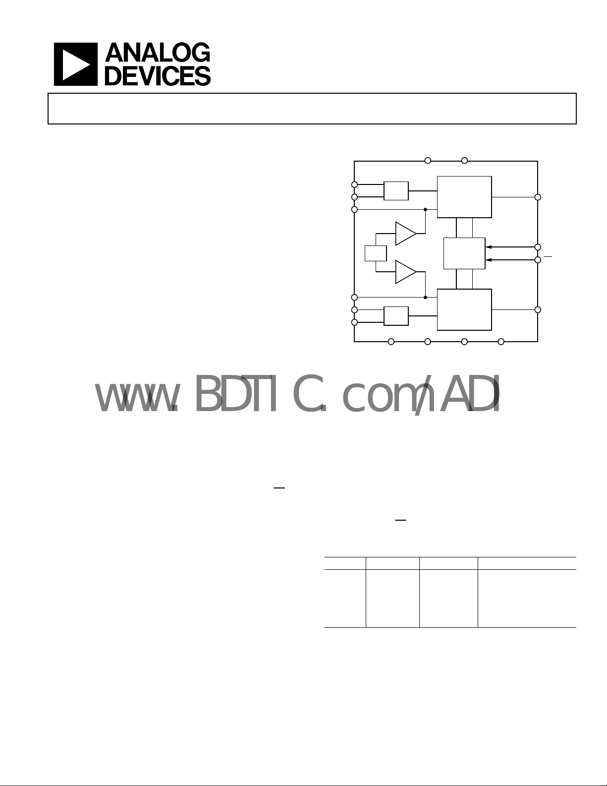
FUNCTIONAL BLOCK DIAGRAM
DRIVE
12-BIT
SUCCESSIVE
APPROXIMATION
ADC
CONTROL
LOGIC
12-BIT
SUCCESSIVE
APPROXIMATION
ADC
Figure 1.
AD7352
SDATA
SCLK
CS
SDATA
07044-001
DGNDREFGNDAGND
V
V
REF
REF
V
V
INA+
INA–
INB+
INB–
DD
T/H
A
BUF
REF
BUF
B
T/H
AGND
B
GENERAL DESCRIPTION
The AD73521 is a dual, 12-bit, high speed, low power, successive
approximation ADC that operates from a single 2.5 V power
supply and features throughput rates up to 3 MSPS. The part
contains two ADCs, each preceded by a low noise, wide bandwidth track-and-hold circuit that can handle input frequencies
in excess of 110 MHz.
The conversion process and data acquisition use standard
control inputs allowing for easy interfacing to microprocessors
or DSPs. The input signal is sampled on the falling edge of
and a conversion is also initiated at this point. The conversion
time is determined by the SCLK frequency.
The AD7352 uses advanced design techniques to achieve very
low power dissipation at high throughput rates. With a 2.5 V
supply and a 3 MSPS throughput rate, the part consumes 10 mA
typically. The part also offers a flexible power/throughput rate
management options.
The analog input range for the part is the differential commonmode ±V
/2. The AD7352 has an on-chip 2.048 V reference
REF
that can be overdriven when an external reference is preferred.
The AD7352 is available in a 16-lead thin shrink small outline
package (TSSOP).
1
Protected by U.S. Patent No. 6,681,332.
CS
;
PRODUCT HIGHLIGHTS
1. Two C omp lete AD C Functions.
These functions allow simultaneous sampling and conversion
of two channels. The conversion result of both channels is
simultaneously available on separate data lines or in succession on one data line if only one serial port is available.
2. High Throughput With Low Power Consumption.
The AD7352 offers a 3 MSPS throughput rate with 26 mW
power consumption.
3. No Conversion Latency.
The AD7352 features two standard successive approximation ADCs with accurate control of the sampling
instant via a
Table 1. Related Devices
Generic Resolution Throughput Analog Input
AD7356 12-bit 5 MSPS Differential
AD7266 12-bit 2 MSPS Differential/single ended
AD7866 12-bit 1 MSPS Single-ended
AD7366 12-bit 1 MSPS Single-ended bipolar
AD7367 14-bit 1 MSPS Single-ended bipolar
CS
input and, once off, conversion control.
Rev. 0
Information furnished by Analog Devices is believed to be accurate and reliable. However, no
responsibility is assumed by Analog Devices for its use, nor for any infringements of patents or other
rights of third parties that may result from its use. Specifications subject to change without notice. No
license is granted by implication or otherwise under any patent or patent rights of Analog Devices.
Trademarks and registered trademarks are the property of their respective owners.
One Technology Way, P.O. Box 9106, Norwood, MA 02062-9106, U.S.A.
Tel: 781.329.4700 www.analog.com
Fax: 781.461.3113 ©2008 Analog Devices, Inc. All rights reserved.

AD7352
www.BDTIC.com/ADI
TABLE OF CONTENTS
Features .............................................................................................. 1
Functional Block Diagram .............................................................. 1
General Description ......................................................................... 1
Product Highlights ........................................................................... 1
Revision History ............................................................................... 2
Specifications ..................................................................................... 3
Timing Specifications .................................................................. 5
Absolute Maximum Ratings ............................................................ 6
ESD Caution .................................................................................. 6
Pin Configuration and Function Descriptions ............................. 7
Typical Performance Characteristics ............................................. 8
Terminology .................................................................................... 10
Theory of Operation ...................................................................... 12
Circuit Information .................................................................... 12
Converter Operation .................................................................. 12
Analog Input Structure .............................................................. 12
Analog Inputs ............................................................................. 13
Driving Differential Inputs ....................................................... 14
ADC Transfer Function ............................................................. 14
Modes of Operation ....................................................................... 15
Normal Mode .............................................................................. 15
Partial Power-Down Mode ....................................................... 15
Full Power-Down Mode ............................................................ 16
Power-Up Times ......................................................................... 17
Power vs. Throughput Rate ....................................................... 17
Serial Interface ................................................................................ 18
Application Hints ........................................................................... 19
Grounding and Layout .............................................................. 19
Evaluating the AD7352 Performance ...................................... 19
Outline Dimensions ....................................................................... 20
Ordering Guide .......................................................................... 20
REVISION HISTORY
10/08—Revision 0: Initial Version
Rev. 0 | Page 2 of 20
AD7352
www.BDTIC.com/ADI
SPECIFICATIONS
IN+
MAX
IN+
DD
and V
1
, unless
and V
IN−
are centered
IN−
VDD = 2.5 V ± 10%, V
= 2.25 V to 3.6 V, internal reference = 2.048 V, f
DRIVE
= 48 MHz, f
SCLK
= 3 MSPS, TA = T
SAMPLE
MIN
to T
otherwise noted.
Table 2.
Parameter Min Typ Max Unit Test Conditions/Comments
DYNAMIC PERFORMANCE fIN = 1 MHz sine wave
Signal-to-Noise Ratio (SNR)
Signal-to-(Noise and Distortion) (SINAD)
Total Harmonic Distortion (THD)
Spurious Free Dynamic Range (SFDR)
Intermodulation Distortion (IMD)
Second-Order Terms −84 dB
Third-Order Terms −76 dB
ADC-to-ADC Isolation
2
CMRR
SAMPLE AND HOLD
Aperture Delay 3.5 ns
Aperture Delay Match 40 ps
Aperture Jitter 16 ps
Full Power Bandwidth
@ 3 dB 110 MHz
@ 0.1 dB 77 MHz
DC ACCURACY
Resolution 12 Bits
Integral Nonlinearity (INL)
Differential Nonlinearity (DNL)
Positive Full-Scale Error
Positive Full-Scale Error Match
Midscale Error
2
Midscale Error Match
Negative Full-Scale Error
Negative Full-Scale Error Match
ANALOG INPUT
Fully Differential Input Range (V
Common-Mode Voltage Range 0.5 1.9 V The voltage around which V
DC Leakage Current ±0.5 ±5 A
Input Capacitance 32 pF When in track mode
8 pF When in hold mode
REFERENCE INPUT/OUTPUT
V
Input Voltage Range 2.048 + 0.1 VDD V
REF
V
Input Current 0.3 0.45 mA When in reference overdrive mode
REF
V
Output Voltage 2.038 2.058 V 2.048 V ± 0.5% max @ VDD = 2.5 V ± 5%
REF
2.043 2.053 V 2.048 V ± 0.25% max @ VDD = 2.5 V ± 5% and 25°C
V
Temperature Coefficient 6 20 ppm/°C
REF
V
Long Term Stability 100 ppm For 1000 hours
REF
V
Thermal Hysteresis
REF
V
Noise 60 V rms
REF
V
Output Impedance 1 Ω
REF
2
2
2
2
2
2
2
2
2
70 71.5 dB
2
69.5 71 dB
−84 −77.5 dB
−85 −78.5 dB
fa = 1 MHz + 50 kHz, fb = 1 MHz − 50 KHz
−100 dB fIN = 1 MHz, f
−100 dB f
= 100 kHz to 2.5 MHz
NOISE
= 100 kHz to 2.5 MHz
NOISE
±0.4 ±1 LSB
±0.5 ±0.99 LSB Guaranteed no missed codes to 12 bits
±1 ±6 LSB
±2 ±8 LSB
+5 0/+11 LSB
2
2
2
and V
IN+
±2 ±8 LSB
±1 ±6 LSB
±2 ±8 LSB
) VCM ± V
IN−
/2 V VCM = common-mode voltage, V
REF
must remain within GND and V
2
50 ppm
Rev. 0 | Page 3 of 20
AD7352
www.BDTIC.com/ADI
Parameter Min Typ Max Unit Test Conditions/Comments
LOGIC INPUTS
Input High Voltage (V
Input Low Voltage (V
Input Current (IIN) ±1 A VIN = 0 V or V
Input Capacitance (CIN) 3 pF
LOGIC OUTPUTS
Output High Voltage (VOH) V
Output Low Voltage (VOL) 0.2 V
Floating-State Leakage Current ±1 A
Floating-State Output Capacitance 5.5 pF
Output Coding Straight binary
CONVERSION RATE
Conversion Time t2 + 13 × t
Track-and-Hold Acquisition Time
Throughput Rate 3 MSPS
POWER REQUIREMENTS
VDD 2.25 2.75 V Nominal VDD = 2.5 V
V
2.25 3.6 V
DRIVE
4
I
TOTAL
Normal Mode (Operational) 10 15 mA
Normal Mode (Static) 6 7.5 mA SCLK on or off
Partial Power-Down Mode 3.5 4.5 mA SCLK on or off
Full Power-Down Mode 5 40 A SCLK on or off, −40°C to +85°C
90 A SCLK on or off, 85°C to 125°C
Power Dissipation
Normal Mode (Operational) 26 45 mW
Normal Mode (Static) 16 21 mW SCLK on or off
Partial Power-Down Mode 9.5 11.5 mW SCLK on or off
Full Power-Down Mode 16 110 W SCLK on or off, −40°C to +85°C
250 W SCLK on or off, 85°C to 125°C
1
Temperature ranges are as follows: Y grade: −40°C to +125°C; B grade: −40°C to +85°C.
2
See the Terminology section.
3
Current and power typical specifications are based on results with VDD = 2.5 V and V
4
I
is the total current flowing in VDD and V
TOTAL
) 0.6 × V
INH
) 0.3 × V
INL
DRIVE
2
3
30 ns Full-scale step input, settling to 0.5 LSBs
V
DRIVE
− 0.2 V
ns
SCLK
Digital inputs = 0 V or V
.
DRIVE
DRIVE
V
DRIVE
= 3.0 V.
DRIVE
DRIVE
Rev. 0 | Page 4 of 20
AD7352
www.BDTIC.com/ADI
TIMING SPECIFICATIONS
VDD = 2.5 V ± 10%, V
= 2.25 V to 3.6 V, internal reference = 2.048 V, TA = T
DRIVE
MAX
Table 3.
Parameter Limit at T
f
50 kHz min
SCLK
MIN
, T
Unit Description
MAX
48 MHz max
t
t
CONVER T
t
5 ns min
QUIET
t2 5 ns min
2
t
3
2,
3
t
4
12.5 ns max
11 ns max
9.5 ns max
9 ns max
+ 13 × t
2
ns max t
SCLK
SCLK
= 1/f
SCLK
Minimum time between end of serial read and next falling edge of CS
to SCLK setup time
CS
6 ns max
Delay from CS
until SDATAA and SDATAB are three-state disabled
Data access time after SCLK falling edge
1.8 V ≤ V
2.25 V ≤ V
2.75 V ≤ V
3.3 V ≤ V
DRIVE
DRIVE
DRIVE
DRIVE
< 2.25 V
< 2.75 V
< 3.3 V
≤ 3.6 V
t5 5 ns min SCLK low pulse width
t6 5 ns min SCLK high pulse width
2
t
3.5 ns min SCLK to data valid hold time
7
2
t
9.5 ns max
8
t9 5 ns min
2
t
4.5 ns min SCLK falling edge to SDATA
10
rising edge to SDATA , SDATAB high impedance
CS
rising edge to falling edge pulse width
CS
A
9.5 ns max SCLK falling edge to SDATAA, SDATAB high impedance
1
Temperature ranges are as follows: Y grade: −40°C to +125°C; B grade: −40°C to +85°C.
2
Specified with a load capacitance of 10 pF on SDATAA and SDATAB.
3
The time required for the output to cross 0.4 V or 2.4 V.
1
to T
, unless otherwise noted.
MIN
, SDATAB high impedance
A
Rev. 0 | Page 5 of 20
AD7352
www.BDTIC.com/ADI
ABSOLUTE MAXIMUM RATINGS
Table 4.
Parameter Rating
VDD to AGND, DGND, REFGND
V
to AGND, DGND, REFGND −0.3 V to +5 V
DRIVE
VDD to V
AGND to DGND to REFGND
Analog Input Voltages1 to AGND
Digital Input Voltages2 to DGND −0.3 V to V
Digital Output Voltages3 to DGND
Input Current to Any Pin Except Supply Pins4 ±10 mA
Operating Temperature Range
Y Grade
B Grade
Storage Temperature Range
Junction Temperature 150°C
TSSOP
θJA Thermal Impedance 143°C/W
θJC Thermal Impedance 45°C/W
Lead Temperature, Soldering
Reflow Temperature (10 sec to 30 sec) 255°C
ESD 1.5 kV
1
Analog input voltages are V
2
Digital input voltages are CS and SCLK.
3
Digital output voltages are SDATAA and SDATAB.
4
Transient currents of up to 100 mA do not cause SCR latch-up.
−5 V to +3 V
DRIVE
, V
, V
INA−
INB+
, V
INA+
−0.3 V to +3 V
−0.3 V to +0.3 V
−0.3 V to V
−0.3 V to V
−40°C to +125°C
−40°C to +85°C
−65°C to +150°C
, REFA, and REFB.
INB−
+ 0.3 V
DD
+ 0.3 V
DRIVE
+ 0.3 V
DRIVE
Stresses above those listed under Absolute Maximum Ratings
may cause permanent damage to the device. This is a stress
rating only; functional operation of the device at these or any
other conditions above those indicated in the operational
section of this specification is not implied. Exposure to absolute
maximum rating conditions for extended periods may affect
device reliability.
ESD CAUTION
Rev. 0 | Page 6 of 20

AD7352
www.BDTIC.com/ADI
PIN CONFIGURATION AND FUNCTION DESCRIPTIONS
Table 5. Pin Function Descriptions
Pin No. Mnemonic Description
1, 2 V
3, 6 REFA, REFB
INA+
, V
Analog Inputs of ADC A. These analog inputs form a fully differential pair.
INA−
Reference Decoupling Capacitor Pins. Decoupling capacitors are connected between these pins and the
REFGND pin to decouple the reference buffer for each respective ADC. It is recommended to decouple each
reference pin with a 10 F capacitor. Provided the output is buffered, the on-chip reference can be taken from
these pins and applied externally to the rest of the system. The nominal internal reference voltage is 2.048 V
and appears at these pins. These pins can also be overdriven by an external reference. The input voltage range
for the external reference is 2.048 V + 100 mV to VDD.
4 REFGND
Reference Ground. This is the ground reference point for the reference circuitry on the AD7352. Any external
reference signal should be referred to this REFGND voltage. Decoupling capacitors must be placed between
this pin and the REF
5, 11 AGND
Analog Ground. This is the ground reference point for all analog circuitry on the AD7352. Refer all analog input
signals to this AGND voltage. The AGND and DGND voltages should ideally be at the same potential and must
not be more than 0.3 V apart, even on a transient basis.
7, 8 V
9 VDD
INB−
, V
Analog Inputs of ADC B. These analog inputs form a fully differential pair.
INB+
Power Supply Input. The V
capacitor in parallel with a 10 µF tantalum capacitor.
10
Chip Select. Active low, logic input. This input provides the dual functions of initiating conversions on the
CS
AD7352 and framing the serial data transfer.
12 DGND
Digital Ground. This is the ground reference point for all digital circuitry on the AD7352. Connect this pin to
the DGND plane of a system. The DGND and AGND voltages should ideally be at the same potential and must
not be more than 0.3 V apart, even on a transient basis.
13, 14 SDATAB, SDATAA
Serial Data Outputs. The data output is supplied to each pin as a serial data stream. The bits are clocked out on
the falling edge of the SCLK input. To access the 12 bits of data from the AD7352, 14 SCLK falling edges are
required. The data simultaneously appears on both data output pins from the simultaneous conversions of
both ADCs. The data stream consists of two leading zeros followed by 12 bits of conversion data. The data is
provided MSB first. If CS
appear after the 12 bits of data. If CS
data from the other ADC follows on the SDATA pins. This allows data from a simultaneous conversion on both
ADCs to be gathered in serial format on either SDATA or SDATA
15 SCLK
Serial Clock, Logic Input. A serial clock input provides the serial clock for accessing the data from the AD7352.
This clock is also used as the clock source for the conversion process.
16 V
DRIVE
Logic Power Supply Input. The voltage supplied at this pin determines at what voltage the interface operates.
The voltage at this pin may be different than the voltage at V
DGND with a 0.1 µF capacitor in parallel with a 10 µF tantalum capacitor.
V
INA+
V
INA–
REF
REFGND
AGND
REF
V
INB–
V
INB+
1
2
3
A
4
5
6
B
7
8
AD7352
TOP VIEW
(Not to Scale)
16
15
14
13
12
11
10
9
V
DRIVE
SCLK
SDATA
SDATA
DGND
AGND
CS
V
DD
A
B
07044-002
Figure 2. Pin Configuration
and REFB pins. Connect the REFGND pin to the AGND plane of a system.
A
range for the AD7352 is 2.5 V ±10%. Decouple the supply to AGND with a 0.1 µF
DD
is held low for 16 SCLK cycles rather than 14 on the AD7352, then two trailing zeros
is held low for a further 16 SCLK cycles on either SDATA or SDATAB, the
. The V
DD
B.
supply should be decoupled to
DRIVE
A
A
Rev. 0 | Page 7 of 20

AD7352
–
www.BDTIC.com/ADI
TYPICAL PERFORMANCE CHARACTERISTICS
0
dB
–20
–40
–60
16,384 POINT FFT
f
= 3MSPS
SAMPLE
f
= 1MHz
IN
SNR = 72.1dB
SINAD = 71.6dB
THD = –81.5dB
60,000
50,000
40,000
30,000
–80
–100
–120
0 150 300 450 600 750 9 00 1050 1200 1350 1500
FREQUENCY (kHz)
Figure 3. Typical FFT
1.0
0.8
0.6
0.4
0.2
0
–0.2
DNL ERROR (LSB)
–0.4
–0.6
–0.8
–1.0
0 500 1000 1500 2000 2500 3000 3500 4000
CODE
Figure 4. Typical DNL Error
20,000
NUMBER OF OCCURRENCES
10,000
07044-003
0
2044 2045 2046 2047 2048 2049 2050
93 HITS 20 HITS
CODE
07044-007
Figure 6. Histogram of Codes for 65,000 Samples
73
72
71
70
69
SNR (dB)
68
67
07044-004
66
0
1000 2000 3000 4000 5000
ANALOG INPUT FREQUENCY (kHz)
07044-035
Figure 7. SNR vs. Analog Input Frequency
1.0
0.8
0.6
0.4
0.2
0
–0.2
INL ERROR (L SB)
–0.4
–0.6
–0.8
–1.0
0 500 1000 1500 2000 2500 3000 3500 4000
CODE
Figure 5. Typical INL Error
07044-005
60
–65
–70
–75
PSRR (dB)
–80
–85
–90
0
5 1015202
SUPPLY RIPPLE FREQUENCY (MHz)
Figure 8. PSRR vs. Supply Ripple Frequency with No Supply Decoupling
Rev. 0 | Page 8 of 20
07044-034
5

AD7352
www.BDTIC.com/ADI
2.0482
2.0480
2.0478
2.0476
2.0474
2.0472
(V)
REF
2.0470
V
2.0468
2.0466
2.0464
2.0462
2.0460
0 500 1000 1500 2000 2500 3000
Figure 9. V
CURRENT LOAD (µA)
vs. Reference Output Current Drive
REF
07044-036
1
1
1
0
)
9
s
n
(
E
M
I
T
8
S
S
E
C
C
7
A
6
5
1.8 2.0 2.2 2.4 2.6 2.8 3.0 3.2 3.4 3.6
+125°C
+85°C
+25°C
–40°C
V
(V)
DRIVE
Figure 12. Access Time vs. V
DRIVE
07044-037
1.0
0.8
0.6
0.4
0.2
0
–0.2
–0.4
LINEARITY ERROR (LSB)
–0.6
–0.8
–1.0
INL MAX
DNL MAX
INL MIN
DNL MIN
0 10203040
SCLK FREQUENCY (kHz)
Figure 10. Linearity Error vs. SCLK Frequency
1.0
0.6
DNL MAX
0.2
INL MAX
07044-023
50
9
+125°C
+85°C
8
7
6
HOLD TIM E (ns)
5
4
1.8 2.0 2.2 2.4 2.6 2.8 3.0 3.2 3.4 3.6
+25°C
–40°C
V
(V)
DRIVE
Figure 13. Hold Time vs. V
DRIVE
07044-038
–0.2
LINEAR ITY E RROR (L SB)
–0.6
–1.0
2.10 2.15 2.20 2.25 2. 30 2.35 2.40 2.45 2.50
EXTERNAL V
Figure 11. Linearity Error vs. External V
DNL MIN
INL MIN
(V)
REF
07044-026
REF
Rev. 0 | Page 9 of 20

AD7352
www.BDTIC.com/ADI
TERMINOLOGY
Integral Nonlinearity (INL)
INL is the maximum deviation from a straight line passing
through the endpoints of the ADC transfer function. The
endpoints of the transfer function are zero scale (1 LSB below
the first code transition) and full scale (1 LSB above the last
code transition).
Differential Nonlinearity (DNL)
DNL is the difference between the measured and the ideal
1 LSB change between any two adjacent codes in the ADC.
Negative Full-Scale Error
Negative full-scale error is the deviation of the first code
transition (00 … 000) to (00 … 001) from the ideal (that is,
−V
+ 0.5 LSB) after the midscale error has been adjusted out.
REF
Negative Full-Scale Error Match
Negative full-scale error match is the difference in negative fullscale error between the two ADCs.
Midscale Error
Midscale error is the deviation of the midscale code transition
(011 … 111) to (100 … 000) from the ideal (that is, 0 V).
Midscale Error Match
Midscale error match is the difference in midscale error
between the two ADCs.
Positive Full-Scale Error
Positive full-scale error is the deviation of the last code
transition (111 … 110) to (111 … 111) from the ideal (that is,
V
− 1.5 LSB) after the midscale error has been adjusted out.
REF
Positive Full-Scale Error Match
Positive full-scale error match is the difference in positive fullscale error between the two ADCs.
ADC-to-ADC Isolation
ADC-to-ADC isolation is a measure of the level of crosstalk
between ADC A and ADC B. It is measured by applying a fullscale 1 MHz sine wave signal to one of the two ADCs and
applying a full-scale signal of variable frequency to the other
ADC. The ADC-to-ADC isolation is defined as the ratio of the
power of the 1 MHz signal on the converted ADC to the power
of the noise signal on the other ADC that appears in the FFT.
The noise frequency on the unselected channel varies from
100 kHz to 2.5 MHz.
Power Supply Rejection Ratio (PSRR)
PSRR is defined as the ratio of the power in the ADC output at
full-scale frequency, f, to the power of a 100 mV p-p sine wave
applied to the ADC V
supply of frequency, fS. The frequency
DD
of the input varies from 5 kHz to 25 MHz.
PSRR (dB) = 10 log(Pf/Pf
)
S
where:
Pf is the power at frequency, f, in the ADC output.
Pf
is the power at frequency, fS, in the ADC output.
S
Rev. 0 | Page 10 of 20
Common-Mode Rejection Ratio (CMRR)
CMRR is defined as the ratio of the power in the ADC output
at full-scale frequency, f, to the power of a 100 mV p-p sine
wave applied to the common-mode voltage of V
of frequency, f
CMRR (dB) = 10 log(Pf/Pf
.
S
)
S
IN+
and V
IN−
where:
Pf is the power at frequency, f, in the ADC output.
Pf
is the power at frequency, fS, in the ADC output.
S
Track-and-Hold Acquisition Time
The track-and-hold amplifier returns to track mode at the end
of a conversion. The track-and-hold acquisition time is the time
required for the output of the track-and-hold amplifier to reach
its final value, within ±0.5 LSB, after the end of a conversion.
Signal-to-(Noise and Distortion) Ratio (SINAD)
SINAD is the measured ratio of signal-to-(noise and distortion)
at the output of the ADC. The signal is the rms amplitude of the
fundamental. Noise is the sum of all nonfundamental signals up
to half the sampling frequency (f
/2), excluding dc. The ratio is
S
dependent on the number of quantization levels in the digitization
process; the more levels, the smaller the quantization noise.
The theoretical SINAD for an ideal N-bit converter with a sine
wave input is given by
SINAD = (6.02 N + 1.76) dB
Thus, for a 12-bit converter, SINAD is 74 dB and for a 14-bit
converter, SINAD is 86 dB.
Total Harmonic Distortion (THD)
THD is the ratio of the rms sum of harmonics to the
fundamental. For the AD7352, it is defined as
22222
++++
VVVVV
65432
THD
()
−=
log20dB
V
1
where:
V
is the rms amplitude of the fundamental.
1
, V3, V4, V5, and V6 are the rms amplitudes of the second
V
2
through the sixth harmonics.
Spurious Free Dynamic Range (SFDR)
SFDR is the ratio of the rms value of the next largest component
in the ADC output spectrum (up to f
/2 and excluding dc) to
S
the rms value of the fundamental. Normally, the value of this
specification is determined by the largest harmonic in the
spectrum, but for ADCs where the harmonics are buried in
the noise floor, it is a noise peak.

AD7352
www.BDTIC.com/ADI
Intermodulation Distortion (IMD)
With inputs consisting of sine waves at two frequencies, fa
and fb, any active device with nonlinearities creates distortion
products at sum and difference frequencies of mfa ± nfb where
m, n = 0, 1, 2, 3, and so on. Intermodulation distortion terms
are those for which neither m nor n is equal to zero. For example,
the second-order terms include (fa + fb) and (fa − fb), while the
third-order terms include (2fa + fb), (2fa − fb), (fa + 2fb), and
(fa − 2fb).
The AD7352 is tested using the CCIF standard where two input
frequencies near the top end of the input bandwidth are used.
In this case, the second-order terms are usually distanced in
frequency from the original sine waves and the third-order
terms are usually at a frequency close to the input frequencies.
As a result, the second- and third-order terms are specified
separately. The calculation of the intermodulation distortion
is as per the THD specification, where it is the ratio of the rms
sum of the individual distortion products to the rms amplitude
of the sum of the fundamentals expressed in decibels.
Thermal Hysteresis
Thermal hysteresis is defined as the absolute maximum change
of reference output voltage after the device is cycled through
temperature from either
T_HYS+ = +25°C to T
T_HYS− = +25°C to T
Thermal hysteresis is expressed in ppm using the following
equation:
)ppm( ×
V
HYS
where:
(25°C) is V
V
REF
(T_HYS) is the maximum change of V
V
REF
or T_HYS–.
=
at 25°C.
REF
to +25°C
MAX
to +25°C
MIN
−°
REF
)_()25(
HYSTVCV
REFREF
)25(
°
CV
at T_HYS+
REF
10
6
Rev. 0 | Page 11 of 20

AD7352
V
V
V
www.BDTIC.com/ADI
THEORY OF OPERATION
CIRCUIT INFORMATION
The AD7352 is a high speed, dual, 12-bit, single-supply,
successive approximation analog-to-digital converter (ADC).
The part operates from a 2.5 V power supply and features
throughput rates of up to 3 MSPS.
The AD7352 contains two on-chip differential track-and-hold
amplifiers, two successive approximation ADCs, and a serial
interface with two separate data output pins. The part is housed
in a 16-lead TSSOP, offering the user considerable space-saving
advantages over alternative solutions.
The serial clock input accesses data from the part but also
provides the clock source for each successive approximation
ADC. The AD7352 has an on-chip 2.048 V reference. If an
external reference is desired, the internal reference can be
overdriven with a reference value ranging from (2.048 V +
100 mV) to V
. If the internal reference is to be used elsewhere
DD
in the system, then the reference output needs to be buffered
first. The differential analog input range for the AD7352 is
V
± V
REF
/2.
CM
The AD7352 features power-down options to allow power
saving between conversions. The power-down feature is
implemented via the standard serial interface, as described
in the Modes of Operation section.
CONVERTER OPERATION
The AD7352 has two successive approximation ADCs, each
based around two capacitive DACs. Figure 14 and Figure 15
show simplified schematics of one of these ADCs in acquisition
phase and conversion phase. The ADC comprises a control
logic, a SAR, and two capacitive DACs. In Figure 14 (the acquisition phase), SW3 is closed, SW1 and SW2 are in Position A,
the comparator is held in a balanced condition, and the sampling
capacitor arrays acquire the differential signal on the input.
CAPACITIVE
DAC
C
B
V
IN+
A
A
V
IN–
B
V
SW1
SW2
REF
S
C
S
Figure 14. ADC Acquisition Phase
COMPARATOR
SW3
CONTROL
LOGIC
CAPACITIVE
DAC
07044-012
When the ADC starts a conversion (see Figure 15), SW3 opens
while SW1 and SW2 move to Position B, causing the comparator
to become unbalanced. Both inputs are disconnected once the
conversion begins. The control logic and charge redistribution
DACs are used to add and subtract fixed amounts of charge
from the sampling capacitor arrays to bring the comparator
back into a balanced condition. When the comparator is
rebalanced, the conversion is complete. The control logic
generates the ADC output code. The output impedances of
the sources driving the V
IN+
and V
pins must be matched;
IN−
otherwise, the two inputs may have different settling times,
resulting in errors.
CAPACITIVE
DAC
C
B
V
IN+
A
A
V
IN–
B
V
SW1
SW2
REF
S
C
S
COMPARATOR
SW3
CONTROL
LOGIC
CAPACITIVE
DAC
07044-013
Figure 15. ADC Conversion Phase
ANALOG INPUT STRUCTURE
Figure 16 shows the equivalent circuit of the analog input structure of the AD7352. The four diodes provide ESD protection for
the analog inputs. Care must be taken to ensure that the analog
input signals never exceed the supply rails by more than 300 mV.
This causes these diodes to become forward biased and start
conducting into the substrate. These diodes can conduct up to
10 mA without causing irreversible damage to the part.
The C1 capacitors in Figure 16 are typically 8 pF and can
primarily be attributed to pin capacitance. The R1 resistors
are lumped components made up of the on resistance of the
switches. The value of these resistors is typically about 30 Ω.
The C2 capacitors are the sampling capacitors of the ADCs
with a capacitance of 32 pF typically.
DD
IN+
D
C1
D
V
DD
C2
R1
IN–
C1
Figure 16. Equivalent Analog Input Circuit,
Conversion Phase—Switches Open,
Track Phase—Switches Closed
Rev. 0 | Page 12 of 20
D
D
C2
R1
07044-015

AD7352
–
–
www.BDTIC.com/ADI
For ac applications, removing high frequency components from
the analog input signal is recommended by the use of an RC
low-pass filter on the analog input pins. In applications where
harmonic distortion and signal-to-noise ratio are critical, the
analog input should be driven from a low impedance source.
Large source impedances significantly affect the ac performance of the ADC and may necessitate the use of an input
buffer amplifier. The choice of the op amp is a function of the
particular application.
When no amplifier is used to drive the analog input, limit
the source impedance to low values. The maximum source
impedance depends on the amount of THD that can be
tolerated. THD increases as the source impedance increases
and performance degrades. Figure 17 shows a graph of THD
vs. the analog input signal frequency for different source
impedances.
65
–67
–69
–71
–73
–75
–77
THD (dB)
–79
–81
–83
–85
–87
–89
100 500 1000 1500 2000 2500
100Ω
FREQUENCY (kHz)
50Ω
33Ω
10Ω
07044-027
Figure 17. THD vs. Analog Input Signal Frequency for Various Source
Impedances
Figure 18 shows a graph of the THD vs. the analog input
frequency while sampling at 3 MSPS. In this case, the source
impedance is 33 Ω.
66
ANALOG INPUTS
Differential signals have some benefits over single-ended
signals, including noise immunity based on the devices
common-mode rejection and improvements in distortion
performance. Figure 19 defines the fully differential input of
the AD7352.
and V
IN+
and V
IN+
to +V
V
IN+
AD7352*
V
IN–
pins in
IN−
should be
IN−
/2. This
REF
, corresponding
REF
07044-039
)
REF
V
p-p
REF
COMMON-MO DE
VOLTAGE
*
ADDITIONAL PINS OMI TTED FO R CLARITY.
V
p-p
REF
Figure 19. Differential Input Definition
The amplitude of the differential signal is the difference
between the signals applied to the V
each differential pair (V
IN+
− V
IN−
). V
simultaneously driven by two signals each of amplitude (V
that are 180° out of phase. This amplitude of the differential
signal is, therefore −V
REF
to +V
peak-to-peak regardless of
REF
the common mode (CM).
CM is the average of the two signals and is, therefore, the
voltage on which the two inputs are centered.
CM = (V
IN+
+ V
IN−
)/2
This results in the span of each input being CM ± V
voltage has to be set up externally. When setting up the CM,
ensure that V
and V
IN+
remain within GND/VDD. When
IN−
a conversion takes place, CM is rejected, resulting in a virtually
noise-free signal of amplitude, −V
REF
to the digital codes of 0 to 4095 for the AD7352.
–70
–74
–78
THD (dB)
–82
–86
–90
0 1000 2000 3000 4000 5000 6000 7000 8000 9000 10000
ANALOG INPUT FREQUENCY (kHz)
07044-028
Figure 18. THD vs. Analog Input Frequency
Rev. 0 | Page 13 of 20

AD7352
V
www.BDTIC.com/ADI
DRIVING DIFFERENTIAL INPUTS
Differential operation requires V
simultaneously with two equal signals that are 180° out of
phase. Because not all applications have a signal preconditioned
for differential operation, there is often a need to perform a
single-ended-to-differential conversion.
Differential Amplifier
An ideal method of applying differential drive to the AD7352
is to use a differential amplifier such as the AD8138. This part
can be used as a single-ended-to-differential amplifier or as a
differential-to-differential amplifier. The AD8138 also provides
common-mode level shifting. Figure 20 shows how the AD8138
can be used as a single-ended-to-differential amplifier. The
positive and negative outputs of the AD8138 are connected to
the respective inputs on the ADC via a pair of series resistors
to minimize the effects of switched capacitance on the front end
of the ADC. The architecture of the AD8138 results in outputs
that are very highly balanced over a wide frequency range
without requiring tightly matched external components.
RG1
V
+2.048V
GND
–2.048V
*MOUNT AS CL OSE TO THE AD7352 AS PO SSIBLE
AND ENSURE THAT HIGH PRECISION R
– 33Ω; RG1 = RF1 = RF2 = 499Ω; CF1 = CF2 = 39pF;
R
S
2 = 523Ω
R
G
51Ω
R
OCM
G
2
Figure 20. Using the AD8138 as a Single-Ended-to-Differential Amplifier
If the analog inputs source being used has zero impedance, all
four resistors (R
1, RG2, RF1, and RF2) should be the same value
G
as each other. If the source has a 50 Ω impedance and a 50 Ω
termination, for example, increase the value of R
balance this parallel impedance on the input and thus ensure
that both the positive and negative analog inputs have the
same gain. The outputs of the amplifier are perfectly matched,
balanced differential outputs of identical amplitude, and are
exactly 180° out of phase.
Op Amp Pair
An op amp pair can be used to directly couple a differential
signal to one of the analog input pairs of the AD7352. The
circuit configurations in Figure 21 and Figure 22 show how an
op amp pair can be used to convert a single-ended signal into
a differential signal for both a bipolar and unipolar input signal,
respectively.
and V
IN+
CF1
RF1
AD8138
2
R
F
2
C
F
10kΩ
10kΩ
RESISTORS ARE USED.
S
IN−
R
*
S
*
R
S
to be driven
2.048V
1.024V
0V
V
IN+
AD7352
V
IN–
2.048V
1.024V
0V
2 by 25 Ω to
G
REF
/REF
A
B
10µF
Rev. 0 | Page 14 of 20
07044-030
The voltage applied to Point A sets up the common-mode
voltage. In both diagrams, it is connected in some way to the
reference. The AD8022 is a suitable dual op amp that could be
used in this configuration to provide differential drive to the
AD7352.
2 × V
p-p
440Ω
220Ω
V+
27Ω
V–
220Ω
220Ω
V+
27Ω
A
V–
10kΩ
REF
REF
GND
*ADDITIONAL PINS OMIT TED FOR CLARI TY.
Figure 21. Dual Op Amp Circuit to Convert a Single-Ended Unipolar Signal
into a Differential Signal
p-p
2 × V
REF
GND
220Ω
*ADDITIONAL PINS OM ITTED F OR CLARIT Y.
440Ω
220Ω
V+
27Ω
V–
220Ω
220Ω
V+
27Ω
A
V–
10kΩ
20kΩ
Figure 22. Dual Op Amp Circuit to Convert a Single-Ended Bipolar Signal into
a Differential Unipolar Signal
2.048V
1.024V
0V
2.048V
1.024V
0V
2.048V
1.024V
0V
2.048V
1.024V
0V
V
IN+
V
IN–
V
IN+
AD7352*
V
IN–
AD7352*
REFA/REF
REFA/REF
B
10µF
B
10µF
ADC TRANSFER FUNCTION
The output coding for the AD7352 is straight binary. The designed
code transitions occur at successive LSB values (1 LSB, 2 LSBs,
and so on). The LSB size is (2 × V
characteristic is shown in Figure 23.
111 ... 111
111 ... 110
111 ... 101
ADC CODE
000 ... 010
000 ... 001
000 ... 000
–V
+ 1 LSB
+ 0.5 LSB
REF
REF
–V
Figure 23. AD7352 Ideal Transfer Characteristic
)/4096. The ideal transfer
REF
– 1.5 LSB
+V
ANALOG INPUT
REF
+V
– 1 LSB
REF
07044-014
07044-031
07044-032

AD7352
A
A
www.BDTIC.com/ADI
MODES OF OPERATION
The mode of operation of the AD7352 is selected by controlling
the logic state of the
CS
signal during a conversion. There are
three possible modes of operation: normal mode, partial powerdown mode, and full power-down mode. After a conversion is
initiated, the point at which
CS
is pulled high determines which
power-down mode, if any, the device enters. Similarly, if already
in power-down mode,
CS
can control whether the device returns
to normal operation or remains in power-down mode.
These modes of operation are designed to provide flexible
power management options. These options can be chosen to
optimize the power dissipation/throughput rate ratio for the
differing application requirements.
NORMAL MODE
Normal mode is intended for applications needing the fastest
throughput rates because the user does not have to worry about
any power-up times because the AD7352 remains fully powered
at all times. Figure 24 shows the general diagram of the
operation of the AD7352 in normal mode.
CS
110 14
SCLK
SDAT
A
SDAT
B
The conversion is initiated on the falling edge of CS, as described
in the section. To ensure that the part remains
Serial Interface
fully powered up at all times,
10 SCLK falling edges have elapsed after the falling edge of
CS
If
is brought high any time after the 10th SCLK falling edge,
but before the 14
up; however, the conversion is terminated and SDATA and
SDATA
go back into three-state. To complete the conversion
B
and access the conversion result for the AD7352, 14 serial clock
cycles are required. The SDATA lines do not return to threestate after 14 SCLK cycles have elapsed but instead do so when
CS
is brought high again. If CS is left low for another two SCLK
cycles, two trailing zeros are clocked out after the data. If
left low for a further 14 SCLK cycles, the result for the other
ADC on board is also accessed on the same SDATA line (see
and the section). Figure 31 Serial Interface
Once 32 SCLK cycles have elapsed, the SDATA line returns to
three-state on the 32
prior to this, the SDATA line returns to three-state at that point.
CS
Thus,
may idle low after 32 SCLK cycles until it is brought
high again sometime prior to the next conversion. The bus still
returns to three-state upon completion of the dual result read.
LEADING ZE ROS + CONVERSION RESULT
Figure 24. Normal Mode Operation
CS
must remain low until at least
th
SCLK falling edge, the part remains powered
A
CS
nd
SCLK falling edge. If CS is brought high
CS
.
is
07044-018
When a data transfer is complete and SDATA
and SDATAB
A
have returned to three-state, another conversion can be initiated
after the quiet time, t
, has elapsed by bringing CS low again
QUIET
(assuming the required acquisition time has been allowed).
PARTIAL POWER-DOWN MODE
Partial power-down mode is intended for use in applications in
which slower throughput rates are required. Either the ADC
is powered down between each conversion or a series of conversions can be performed at a high throughput rate, and the ADC
is then powered between these bursts of several conversions. It
is recommended that the AD7352 not remain in partial powerdown mode for longer than 100 μs. When the AD7352 is in
partial power-down, all analog circuitry is powered down
except for the on-chip reference and reference buffers.
To enter partial power-down mode, the conversion process
must be interrupted by bringing
second falling edge of SCLK and before the 10
SCLK, as shown in . When Figure 25
in this window of SCLKs, the part enters partial power-down,
the conversion that was initiated by the falling edge of
terminated, and SDATA
CS
is brought high before the second SCLK falling edge, the
If
A
part remains in normal mode and does not power down. This
avoids accidental power-down due to glitches on the
CS
SCLK
SDATA
SDATA
A
B
1110 42
Figure 25. Entering Partial Power-Down Mode
To exit this mode of operation and power up the AD7352 again,
perform a dummy conversion. The device begins to power up
on the falling edge of
CS
is held low until after the falling edge of the 10th SCLK. The
CS
and continues to power up as long as
device is fully powered up after approximately 333 ns have
elapsed (or one full conversion), and valid data results from
the next conversion, as shown in . If Figure 26
high before the second falling edge of SCLK, the AD7352 again
goes into partial power-down. This avoids accidental power-up
due to glitches on the
CS
power up on the falling edge of
rising edge of
mode and
CS
. If the AD7352 is already in partial power-down
CS
is brought high between the second and 10th
falling edges of SCLK, the device enters full power-down mode.
CS
high any time after the
CS
th
falling edge of
has been brought high
CS
is
and SDATAB go back into three-state.
CS
line.
THREE-STATE
CS
is brought
line. Although the device may begin to
CS
, it powers down again on the
07044-019
Rev. 0 | Page 15 of 20

AD7352
S
A
S
A
www.BDTIC.com/ADI
FULL POWER-DOWN MODE
Full power-down mode is intended for use in applications
where throughput rates slower than those in partial powerdown mode are required because power-up from a full powerdown takes substantially longer than that from a partial powerdown. This mode is more suited to applications in which a
series of conversions performed at a relatively high throughput
rate are followed by a long period of inactivity and, thus, powerdown. When the AD7352 is in full power-down mode, all
analog circuitry is powered down including the on-chip
reference and reference buffers. Full power-down mode is
entered in a similar way as partial power-down mode, except
that the timing sequence shown in Figure 25 must be executed
twice. The conversion process must be interrupted in a similar
fashion by bringing
edge of SCLK and before the 10
device enters partial power-down mode at this point.
CS
high anywhere after the second falling
th
falling edge of SCLK. The
To reach full power-down mode, the next conversion cycle must
be interrupted in the same way, as shown in Figure 27. When
CS
is brought high in this window of SCLKs, the part fully
powers down. Note that it is not necessary to complete the 14 or
16 SCLKs once
CS
has been brought high to enter a power-
down mode.
To exit full power-down mode and power-up the AD7352,
perform a dummy conversion, similar to powering up from
partial power-down. On the falling edge of
power up as long as
th
the 10
SCLK. The required power-up time must elapse before
CS
is held low until after the falling edge of
CS
, the device begins to
a conversion can be initiated, as shown in . Figure 28
THE PART IS F ULLY PO WERED UP;
SEE THE POWER-UP TIMES SECTION.
VALID DATA
07044-020
SCLK
SDATA
SDATA
CS
A
B
THE PART BEGI NS
TO POW ER UP.
11014 141
t
POWER-UP1
INVALID DATA
Figure 26. Exiting Partial Power-Down Mode
THE PART BEGI NS
TO POWER UP.
1102
THE PART ENTERS
FULL PO WER-DOWN MODE.
INVALID DATAINVALID DATA
THREE-STATE
14
07044-021
SCLK
DAT
DAT
CS
THE PART ENTERS
PARTIAL PO WER-DOWN M ODE.
110142
A
B
THREE-STATE
Figure 27. Entering Full Power-Down Mode
THE PART IS FULLY PO WERED UP;
SEE THE POWER-UP TIMES SECTION.
CS
THE PART BEGI NS
TO POW ER UP.
t
POWER-UP2
SCLK
SDATA
SDATA
1
A
B
INVALID DATA VALID DATA
10 14 141
Figure 28. Exiting Full Power-Down Mode
Rev. 0 | Page 16 of 20
07044-022

AD7352
www.BDTIC.com/ADI
POWER-UP TIMES
The AD7352 has two power-down modes: partial power-down
and full power-down, which are described in detail in the
Normal Mode, Partial Power-Down Mode, and Full PowerDown Mode sections. This section deals with the power-up
time required when coming out of any of these modes. Note
that the recommended decoupling capacitors must be in place
on the REF
To power up from partial power-down mode, one dummy cycle
is required. The device is fully powered up after approximately
333 ns have elapsed from the falling edge of
power-up time has elapsed, the ADC is fully powered up, and
the input signal is acquired properly. The quiet time, t
must still be allowed from the point where the bus goes back
into three-state after the dummy conversion to the next falling
edge of
To power up from full power-down mode, approximately
6 ms should be allowed from the falling edge of
in as t
Note that during power-up from partial power-down mode, the
track-and-hold, which is in hold mode while the part is powered
down, returns to track mode after the first SCLK edge that the
part receives after the falling edge of
When power supplies are first applied to the AD7352, the ADC
can power up in either of the power-down modes or in normal
mode. Because of this, it is best to allow a dummy cycle to elapse
to ensure that the part is fully powered up before attempting a
valid conversion. Likewise, if the part is to be kept in partial
power-down mode immediately after the supplies are applied,
then two dummy cycles must be initiated. The first dummy
cycle must hold
the second cycle,
and 10
and REFB pins for the power-up times to apply.
A
CS
. When the partial
CS
.
POWER-UP2
CS
th
SCLK falling edges (see ). Figure 25
. Figure 28
CS
.
low until after the 10th SCLK falling edge; in
CS
must be brought high between the second
CS
, shown
QUIET
,
Alternatively, if the part is to be placed into full power-down
mode when the supplies are applied, three dummy cycles must
be initiated. The first dummy cycle must hold
th
the 10
SCLK falling edge; the second and third dummy cycles
place the part into full power-down mode (see and
the section).
Modes of Operation
CS
low until after
Figure 27
POWER vs. THROUGHPUT RATE
The power consumption of the AD7352 varies with the
throughput rate. When using very slow throughput rates and
as fast an SCLK frequency as possible, the various power-down
options can be used to make significant power savings. However,
the AD7352 quiescent current is low enough that, even without
using the power-down options, there is a noticeable variation in
power consumption with sampling rate. This is true whether a
fixed SCLK value is used or it is scaled with the sampling
rate. Figure 29 shows a plot of power vs. throughput rate when
operating in normal mode for a fixed maximum SCLK frequency
and a SCLK frequency that scales with the sampling rate. The
internal reference was used for Figure 29.
30
28
26
24
22
80MHz SCLK
20
18
POWER (mW)
16
14
12
10
0 1000 2000 3000
Figure 29. Power vs. Throughput Rate
VARIABLE SCLK
THROUGHPUT (kSPS)
07044-029
Rev. 0 | Page 17 of 20

AD7352
www.BDTIC.com/ADI
SERIAL INTERFACE
Figure 30 shows the detailed timing diagram for serial
interfacing to the AD7352. The serial clock provides the
conversion clock and controls the transfer of information
from the AD7352 during conversion.
CS
The
signal initiates the data transfer and conversion process.
The falling edge of
CS
puts the track and hold into hold mode,
at which point the analog input is sampled and the bus is taken
out of three-state. The conversion is also initiated at this point
and requires a minimum of 14 SCLKs to complete. Once
13 SCLK falling edges have elapsed, the track and hold goes
back into track on the next SCLK rising edge, as shown in
Figure 30
at Point B. If a 16-bit data transfer is used on the
AD7352, then two trailing zeros appear after the final LSB. On
the rising edge of
and SDATA
CS
, the conversion is terminated and SDATA
go back into three-state. If
B
CS
is not brought high,
but is instead held low for an additional 14 SCLK cycles, the
data from the conversion on ADC B is output on SDATA
Figure 31
). Likewise, the data from the conversion on ADC A is
(see
A
A
output on SDATA
back into three-state on the 32
CS
edge of
, whichever occurs first.
. In this case, the SDATA line in use goes
B
nd
SCLK falling edge or the rising
A minimum of 14 serial clock cycles is required to perform
the conversion process and to access data from one conversion
on either data line of the AD7352.
CS
falling low provides the
leading zero to be read in by the microcontroller or DSP. The
remaining data is then clocked out by subsequent SCLK falling
edges, beginning with a second leading zero. Thus, the first falling
clock edge on the serial clock has the leading zero provided and
also clocks out the second leading zero. The 12-bit result then
follows with the final bit in the data transfer and is valid on the
th
14
falling edge (having been clocked out on the previous (13th)
falling edge). In applications with a slower SCLK, it may be
possible to read in data on each SCLK rising edge, depending
on the SCLK frequency. With a slower SCLK, the first rising
edge of SCLK after the
zero provided, and the 13
CS
falling edge has the second leading
th
rising SCLK edge has DB0 provided.
t
ACQUISI TION
CS
t
QUIET
t
9
07044-024
SCLK
SDATA
SDATA
A
B
THREESTATE
t
2
1
t
3
00 DB1
2 LEADING ZEROS
t
CONVERT
t
6
2
34
DB11 DB10 DB2 DB0
5
t
7
t
4
DB9 DB8
13
t
5
B
t
8
THREE-STATE
Figure 30. Serial Interface Timing Diagram
CS
t
6
5
t
5
t
4
A
15
14
t
7
2 TRAILING ZEROS
16
17
ZEROZERO ZERO
2 LEADING ZE ROS
DB11
32
t
10
B
ZERO ZERO
2 TRAILING ZEROS
THREESTATE
07044-025
SCLK
SDATA
A
THREESTATE
t
2
1
t
3
00 ZERO
2 LEADING
ZEROS
2
DB11
A
34
DB10ADB9
Figure 31. Reading Data from Both ADCs on One SDATA Line with 32 SCLKs
Rev. 0 | Page 18 of 20

AD7352
www.BDTIC.com/ADI
APPLICATION HINTS
GROUNDING AND LAYOUT
The analog and digital supplies to the AD7352 are independent
and separately pinned out to minimize coupling between the
analog and digital sections of the device. The printed circuit
board (PCB) that houses the AD7352 should be designed so
that the analog and digital sections are separated and confined
to certain areas of the board. This design facilitates the use of
ground planes that can be easily separated.
To provide optimum shielding for ground planes, a minimum
etch technique is generally best. The two AGND pins of the
AD7352 should be sunk in the AGND plane. The REFGND
pin should also be sunk in the AGND plane. Digital and analog
ground planes should be joined in only one place. If the
AD7352 is in a system in which multiple devices require an
AGND and DGND connection, the connection should still
be made at one point only, a star ground point should be
established as close as possible to the ground pins on the
AD7352.
Avoid running digital lines under the device because this couples
noise onto the die. Allow the analog ground planes to run under
the AD7352 to avoid noise coupling. The power supply lines to
the AD7352 should use as large a trace as possible to provide
low impedance paths and reduce the effects of glitches on the
power supply line.
To avoid radiating noise to other sections of the board, shield
fast switching signals such as clocks, with digital ground, and
never run clock signals near the analog inputs. Avoid crossover
of digital and analog signals. To reduce the effects of
feedthrough within the board, traces on opposite sides of the
board should run at right angles to each other. A microstrip
technique is the best method but is not always possible with a
double-sided board. In this technique, the component side of
the board is dedicated to ground planes and signals are placed
on the solder side.
Good decoupling is important; decouple all supplies with 10 μF
tantalum capacitors in parallel with 0.1 μF capacitors to GND.
To achieve the best results from these decoupling components,
they must be placed as close as possible to the device, ideally
right up against the device. The 0.1 μF capacitor, (including the
common ceramic types or surface-mount types) should have
low effective series resistance (ESR) and effective series
inductance (ESI). These low ESR and ESI capacitors provide a
low impedance path to ground at high frequencies to handle
transient currents due to logic switching.
EVALUATING THE AD7352 PERFORMANCE
The recommended layout for the AD7352 is outlined in the
evaluation board documentation. The evaluation board package
includes a fully assembled and tested evaluation board, documentation, and software for controlling the board from the PC via
the converter evaluation and development board (CED). The
CED can be used in conjunction with the AD7352 evaluation
board (as well as many other Analog Devices, Inc., evaluation
boards ending in the ED designator) to demonstrate/evaluate
the ac and dc performance of the AD7352.
The software allows the user to perform ac (fast Fourier transform)
and dc (linearity) tests on the AD7352. The software and documentation are on a CD shipped with the evaluation board.
Rev. 0 | Page 19 of 20

AD7352
www.BDTIC.com/ADI
OUTLINE DIMENSIONS
5.10
5.00
4.90
0.15
0.05
4.50
4.40
4.30
PIN 1
16
0.65
BSC
COPLANARITY
COMPLIANT TO JEDEC STANDARDS MO-153-AB
0.10
0.30
0.19
9
81
1.20
MAX
SEATING
PLANE
6.40
BSC
0.20
0.09
8°
0°
0.75
0.60
0.45
Figure 32. 16-Lead Thin Shrink Small Outline Package [TSSOP]
(RU-16)
Dimensions shown in millimeters
ORDERING GUIDE
Model Temperature Range Package Description Package Option
AD7352BRUZ
AD7352BRUZ-500RL7
AD7352BRUZ-RL
AD7352YRUZ
AD7352YRUZ-500RL7
AD7352YRUZ-RL
EVAL-AD7352EDZ
EVAL-CED1Z
1
Z = RoHS Compliant Part.
2
This evaluation board can be used as a standalone evaluation board or in conjunction with the EVAL-CED1Z board for evaluation/demonstration purposes
3
This evaluation board is a complete unit allowing a PC to control and communicate with all Analog Devices evaluation boards ending in the ED designator.
1
1
−40°C to +85°C 16-Lead TSSOP RU-16
1
−40°C to +85°C 16-Lead TSSOP RU-16
1
−40°C to +125°C 16-Lead TSSOP RU-16
1
−40°C to +125°C 16-Lead TSSOP RU-16
1
−40°C to +125°C 16-Lead TSSOP RU-16
1, 2
Evaluation Board
1, 3
Converter Evaluation and Development Board
−40°C to +85°C 16-Lead TSSOP RU-16
©2008 Analog Devices, Inc. All rights reserved. Trademarks and
registered trademarks are the property of their respective owners.
D07044-0-10/08(0)
Rev. 0 | Page 20 of 20
 Loading...