

Low Voltage, 10-Bit Digital Temperature
www.BDTIC.com/ADI
a
FEATURES
10-Bit Temperature-to-Digital Converter
–35C to +85C Operating Temperature Range
2C Accuracy
SPI® and DSP Compatible Serial Interface
Shutdown Mode
Space-Saving MSOP Package
APPLICATIONS
Hard Disk Drives
Personal Computers
Electronic Test Equipment
Office Equipment
Domestic Appliances
Process Control
Mobile Phones
GENERAL DESCRIPTION
The AD7314 is a complete temperature monitoring system in
an 8-lead MSOP package. It contains a band gap temperature
sensor and 10-bit ADC to monitor and digitize the temperature
reading to a resolution of 0.25∞C.
The AD7314 has a flexible serial interface that allows easy
interfacing to most microcontrollers. The interface is compatible with SPI, QSPI™, and MICROWIRE™ protocols and is
also compatible with DSPs. The part features a standby mode
that is controlled via the serial interface.
The AD7314’s low supply current and SPI compatible interface
make it ideal for a variety of applications, including personal
computers, office equipment, and domestic appliances.
Sensor in 8-Lead MSOP
AD7314
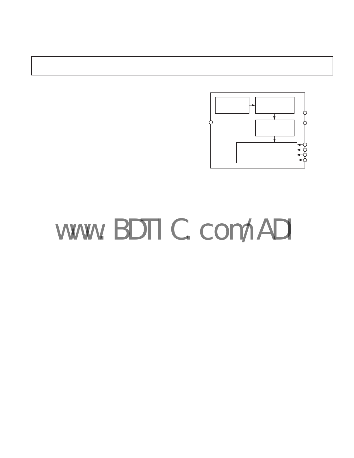
FUNCTIONAL BLOCK DIAGRAM
BAND GAP
TEMPERATURE
SENSOR
GND
AD7314
PRODUCT HIGHLIGHTS
1. The AD7314 has an on-chip temperature sensor that allows
an accurate measurement of the ambient temperature. The
measurable temperature range is –35∞C to +85∞C, with a
± 2∞C temperature accuracy.
2. Supply voltage of 2.65 V to 5.5 V.
3. Space-saving 8-lead MSOP package.
4. 10-bit temperature reading to 0.25∞C resolution.
5. The AD7314 features a standby mode that reduces the
current consumption to 1 mA max.
10-BIT
ANALOG-TO-DIGITAL
CONVERTER
TEMPERATURE
VALUE
REGISTER
SERIAL
BUS
INTERFACE
ID
V
DD
CE
SCLK
SDI
SDO
REV. A
Information furnished by Analog Devices is believed to be accurate and
reliable. However, no responsibility is assumed by Analog Devices for its
use, nor for any infringements of patents or other rights of third parties that
may result from its use. No license is granted by implication or otherwise
under any patent or patent rights of Analog Devices. Trademarks and
registered trademarks are the property of their respective owners.
One Technology Way, P.O. Box 9106, Norwood, MA 02062-9106, U.S.A.
Tel: 781/329-4700 www.analog.com
Fax: 781/326-8703 © 2003 Analog Devices, Inc. All rights reserved.

AD7314–SPECIFICATIONS
www.BDTIC.com/ADI
(TA = T
MIN
to T
, VDD = 2.65 V to 5.5 V, unless otherwise noted.)
MAX
*
Parameter Min Typ Max Unit Test Conditions/Comments
TEMPERATURE SENSOR AND ADC
Accuracy ± 2.0 ∞CT
± 1.0 ∞CT
= –35∞C to +85∞C. VDD = 2.65 V to 2.9 V
A
= –35∞C to +85∞C. VDD = 3 V to 5.5 V
A
Resolution 10 Bits
Update Rate, t
R
400 ms
Temperature Conversion Time 25 ms
SUPPLIES
Supply Voltage 2.65 5.5 V For Specified Performance
Supply Current
Normal Mode (Inactive) 250 300 mA Part Not Converting, V
275 mA Part Not Converting, V
Normal Mode (Active) 1 mA Part Converting, V
1.2 mA Part Converting, V
Shutdown Mode 1 mAV
1 mAV
Power Dissipation 860 mWV
= 2.65 V to 2.9 V
DD
= 3 V to 5.5 V
DD
= 2.65 V. Using Normal Mode
DD
= 2.65 V to 2.9 V
DD
= 3 V to 5.5 V
DD
= 2.65 V to 2.9 V
DD
= 3 V to 5.5 V
DD
(Auto Conversion)
Power Dissipation V
= 2.65 V. Using Shutdown Mode
DD
1 SPS 3 mW
10 SPS 3.3 mW
100 SPS 6 mW
DIGITAL INPUT
Input High Voltage, V
Input Low Voltage, V
IL
Input High Voltage, V
Input Low Voltage, V
Input Current, I
Input Capacitance, C
IL
IN
IN
IH
IH
1.85 V VDD = 2.65 V to 2.9 V
0.53 V VDD = 2.65 V to 2.9 V
2.4 V VDD = 3 V to 5.5 V
0.8 V VDD = 3 V to 5.5 V
± 1 mAV
= 0 V to V
IN
DD
10 pF All Digital Inputs
DIGITAL OUTPUT
Output High Voltage, V
Output Low Voltage, V
Output Capacitance, C
*All specifications apply for –35∞C to +85∞C, unless otherwise noted.
Specifications subject to change without notice.
OH
OL
OUT
2.4 V I
0.4 V IOL = 200 mA
50 pF
SOURCE
= I
SINK
= 200 mA
TIMING CHARACTERISTICS
1, 2
3
(T
= T
to T
A
MIN
, VDD = 2.65 V to 5.5 V, unless otherwise noted. See Figure 1.)
MAX
Parameter Limit Unit Comments
t
1
t
2
t
3
4
t
4
t
5
t
6
t
7
4
t
8
NOTES
1
Guaranteed by design and characterization, not production tested.
2
All input signals are specified with tr = tf = 5 ns (10% to 90% of VDD) and are timed from a voltage level of 1.6 V.
3
All specifications apply for –35∞C to +85∞C, unless otherwise noted.
4
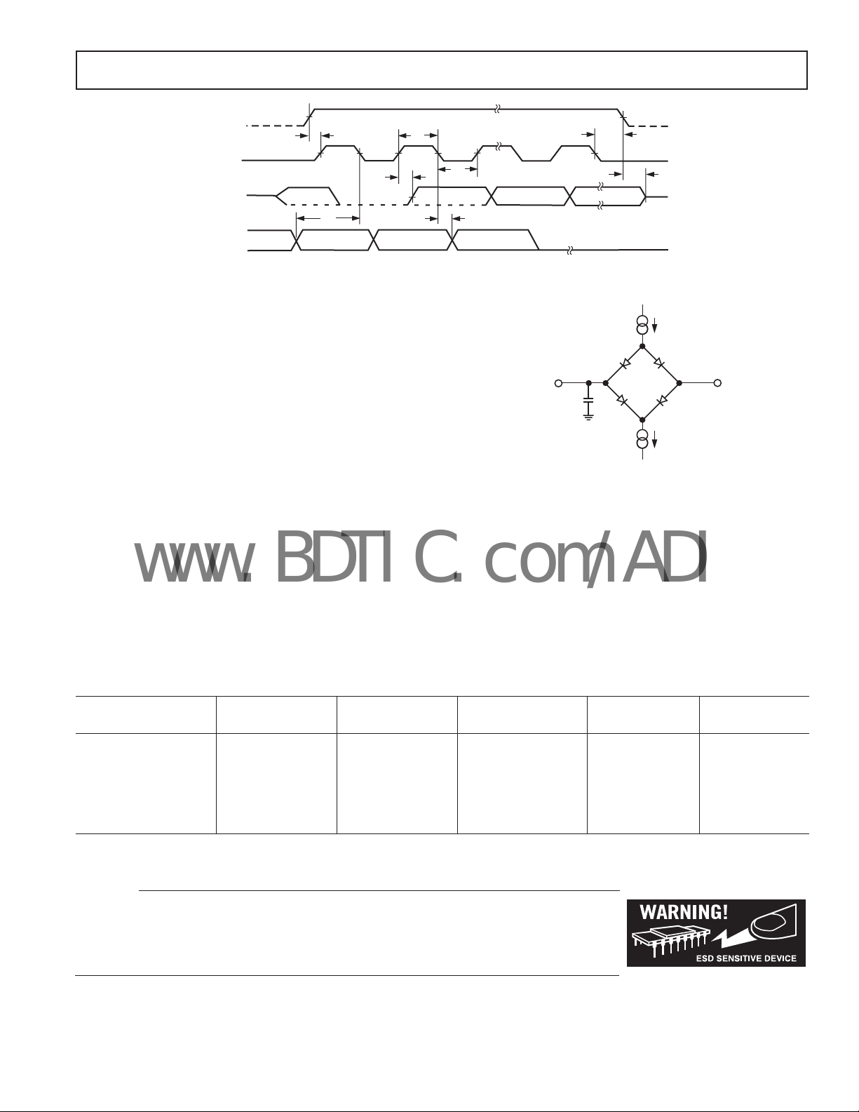
Measured with the load circuit of Figure 2.
Specifications subject to change without notice.
0 ns min CE to SCLK Setup Time
50 ns min SCLK High Pulse Width
50 ns min SCLK Low Pulse Width
35 ns max Data Access Time after SCLK Rising Edge
20 ns min Data Setup Time prior to SCLK Falling Edge
0 ns min Data Hold Time after SCLK Falling Edge
0 ns min CE to SCLK Hold Time
40 ns max CE to SDO High Impedance
–2–
REV. A
CE
www.BDTIC.com/ADI
SCLK
SDO
SDI
AD7314
t
1
t
5
t
2
t
t
4
3
t
6
Figure 1. Timing Diagram
t
7
t
8
ABSOLUTE MAXIMUM RATINGS
VDD to GND . . . . . . . . . . . . . . . . . . . . . . . . . . –0.3 V to +7 V
Digital Input Voltage to GND . . . . . . . –0.3 V to V
Digital Output Voltage to GND . . . . . –0.3 V to V
Operating Temperature Range . . . . . . . . . . . –35°C to +85°C
Storage Temperature Range . . . . . . . . . . . . –65°C to +150°C
Junction Temperature . . . . . . . . . . . . . . . . . . . . . . . . . 150°C
1
+ 0.3 V
DD
+ 0.3 V
DD
TO
OUTPUT
PIN
50pF
C
L
200AI
OL
1.6V
MSOP Package, Power Dissipation . . . . . . . . . . . . . . 450 mW
Thermal Impedance . . . . . . . . . . . . . . . . . . . . 206°C/W
θ
JA
Lead Temperature, Soldering
200AI
OH
Vapor Phase (60 sec) . . . . . . . . . . . . . . . . . . . . . . 215°C
Infrared (15 sec) . . . . . . . . . . . . . . . . . . . . . . . . . . 220°C
Latch-Up for ID Pin
2
. . . . . . . . . . . . . . . . . . . . . . . . ≤ –70 mA
Figure 2. Load Circuit for Data Access Time and Bus
Relinquish Time
Latch-Up for All Other Pins . . . . . . . . . . . . . . . . . ≥ –110 mA
NOTES
1
Stresses above those listed under Absolute Maximum Ratings may cause perma-
nent damage to the device. This is a stress rating only; functional operation of the
device at these or any other conditions above those indicated in the operational
section of this specification is not implied. Exposure to absolute maximum rating
conditions for extended periods may affect device reliability.
2
Correct usage of the ID pin will prevent any latch-up from occurring. In an
application, the ID pin should be either tied to V
circuit. If the application complies with this recommendation, the ID pin will never
see –70 mA.
via a 100 kΩ resistor or left open
DD
ORDERING GUIDE
Temperature Temperature Package Package
Model Range Error Description Option Branding
AD7314ARM –35°C to +85°C ±2°C 8-Lead MSOP RM-8 CKA
AD7314ARM-REEL –35°C to +85°C ± 2°C 8-Lead MSOP RM-8 CKA
AD7314ARM-REEL7 –35°C to +85°C ±2°C 8-Lead MSOP RM-8 CKA
AD7314ARMZ* –35°C to +85°C ± 2°C 8-Lead MSOP RM-8 CKA
AD7314ARMZ-REEL* –35°C to +85°C ±2°C 8-Lead MSOP RM-8 CKA
AD7314ARMZ-REEL7* –35°C to +85°C ± 2°C 8-Lead MSOP RM-8 CKA
*Z = Lead Free.
CAUTION
ESD (electrostatic discharge) sensitive device. Electrostatic charges as high as 4000 V readily
accumulate on the human body and test equipment and can discharge without detection. Although
the AD7314 features proprietary ESD protection circuitry, permanent damage may occur on
devices subjected to high energy electrostatic discharges. Therefore, proper ESD precautions are
recommended to avoid performance degradation or loss of functionality.
REV. A
–3–

AD7314
www.BDTIC.com/ADI
PIN CONFIGURATION
8-Lead MSOP
NC
1
CE
2
SCLK
3
GND
4
NC = NO CONNECT
AD7314
TOP VIEW
(Not to Scale)
V
8
DD
ID
7
SDI
6
SDO
5
PIN FUNCTION DESCRIPTIONS
Pin No. Mnemonic Description
1NCNo Connect.
2CEChip Enable Input. The device is selected when this input is high. The SCLK input is disabled
when this pin is low.
3 SCLK Serial Clock Input. This is the clock input for the serial port. The serial clock is used to clock
data out of the temperature value register of the AD7314 and also to clock data into the control
register on the part.
4 GND Analog and Digital Ground.
5SDO Serial Data Output. Logic output. Data is clocked out of the temperature value register at this pin.
6 SDI Serial Data Input. Serial data to be loaded to the parts’s control register is provided on this input.
7IDIdentification. This pin can be used by a master device to identify the AD7314 in an SPI bus
system. This pin has an internal pull-down resistor of 1 kW.
8VDDPositive Supply Voltage, 2.65 V to 5.5 V.
–4–
REV. A

AD7314
www.BDTIC.com/ADI
CIRCUIT INFORMATION
The AD7314 is a 10-bit digital temperature sensor. The part
houses an on-chip temperature sensor, a 10-bit A/D converter,
and reference and serial interface logic functions in an MSOP
package. The A/D converter section consists of a conventional
successive approximation converter based around a capacitor
DAC. The parts are capable of running on a 2.65 V to 5.5 V
power supply.
The on-chip temperature sensor allows an accurate measurement
of the ambient device temperature to be made. The working
measurement range of the AD7314 is –35∞C to +85∞C.
CONVERTER DETAILS
The conversion clock for the part is internally generated so no
external clock is required except when reading from and writing
to the serial port. In normal mode, an internal clock oscillator
runs the automatic conversion sequence. A conversion is initiated every 400 ms. At this time, the part wakes up and performs
a temperature conversion. This temperature conversion typically
takes 25 ms, at which time the part automatically shuts down.
The result of the most recent temperature conversion is available in the serial output register at any time. The AD7314 can
be placed in a shutdown mode, via the control register, in
which case the on-chip oscillator is shut down and no further
conversions are initiated until the AD7314 is taken out of shutdown mode. The conversion result from the last conversion prior
to shutdown can still be read from the AD7314 even when it is
in shutdown mode.
In the automatic conversion mode, every time a read or write
operation takes place, the internal clock oscillator is restarted at
the end of the read or write operation. The result of the conversion is available, typically 25 ms later. Similarly, when the part is
taken out of shutdown mode, the internal clock oscillator is
restarted and the conversion result is available, typically 25 ms
later. Reading from the device again before conversion is complete will provide the same set of data.
Temperature Value Register
The temperature value register is a read-only register that stores
the temperature reading from the ADC in 10-bit twos complement format. The temperature data format is shown in Table I.
This shows the full theoretical range of the ADC from –128∞C
to +127∞C, but in practice the temperature measurement range
is limited to the operating temperature range of the device (–35∞C
to +85∞C).
Table I. Temperature Data Format
Digital Output
Temperature (C) DB9 . . . DB0
–128 10 0000 0000
–125 10 0000 1100
–100 10 0111 0000
–75 10 1101 0100
–50 11 0011 1000
–25 11 1001 1100
–0.25 11 1111 1111
0 00 0000 0000
0.25 00 0000 0001
10 00 0010 1000
25 00 0110 0100
50 00 1100 1000
75 01 0010 1100
100 01 1001 0000
125 01 1111 0100
127 01 1111 1100
Serial Interface
The serial interface on the AD7314 consists of four wires, CE,
SCLK, SDI, and SDO. The interface can be operated in 3-wire
mode with SDI tied to ground, in which case the interface has
read-only capability, with data being read from the data register
via the SDO line. The SDI line is used to write the part into
standby mode, if required. The CE line is used to select the
device when more than one device is connected to the serial
clock and data lines. To ensure that the serial port is reset properly after power-up, the CE must be at a logic low before the
first serial port access. The serial clock is active only when CE is
high. For correct data synchronization, it is important that the
CE be low when the serial port is not being accessed.
The part operates in a slave mode and requires an externally
applied serial clock to the SCLK input to access data from the
data register. The serial interface on the AD7314 is designed to
allow the part to be interfaced to systems that provide a serial
clock that is synchronized to the serial data, such as the 80C51,
87C51, 68HC11, 68HC05, and PIC16Cxx microcontrollers as
well as DSP processors.
A read operation from the AD7314 accesses data from the
temperature value register while a write operation to the part
writes data to the control register. Input data is not loaded into
the control register until the rising edge of the 15th SCLK cycle.
Data on the SDI line is latched in on the falling edge of the
serial clock while data is updated on the SDO line on the rising
edge of the serial clock.
Read Operation
Figure 3 shows the interface diagram for a serial read from the
AD7314. The CE line enables the SCLK input. A leading zero
and 10 bits of data are transferred during a read operation. Read
operations occur during streams of 16 clock pulses. Output data
is updated on the rising edge of SCLK. The serial data is accessed
in a number of bytes if 10 bits of data are being read. At the end
of the read operation, the SDO line remains in the state of the
last bit of data clocked out of the AD7314 until CE returns low,
at which time the SDO line goes into three-state.
REV. A
–5–

AD7314
www.BDTIC.com/ADI
CE
DB9
t
6
3
POWER-
DOWN
4
DB8 DB0
SCLK
SDO
SDI
12
t
4
LEADING
ZERO
DON'T
CARE
DON'T
CARE
Figure 3. Serial Interface Diagram
Write Operation
Figure 3 also shows the interface diagram for a serial write to
the AD7314. The write operation takes place at the same time
as the read operation. Data is clocked into the control register
on the falling edge of SCLK. Only the third bit in the data stream
provides a user-controlled function. This third bit is the powerdown bit which, when set to a 1, puts the AD7314 into shutdown
mode. The first two bits of the data stream are don’t cares while
all other bits in the data stream other than the power-down bit
should be 0 to ensure correct operation of the AD7314. Data is
loaded into the control register on the 15th rising SCLK edge.
The data takes effect at this time, i.e., if the part is programmed
to go into shutdown, it does so at this point. If the CE is brought
low before this 15th SCLK edge, the control register will not be
loaded and the power-down status of the part will not change.
MICROCONTROLLER INTERFACING
The AD7314 serial interface allows for easy interface to most
microcontrollers and microprocessors. A typical interface circuit
is shown in Figure 4.
AD7314*
SCLK
SDI
SDO
CE
*ADDITIONAL PINS OMITTED FOR CLARITY
CONTROLLER*
SCLK
DOUT
DIN
CE
Figure 4. Typical Interface
The ID pin of the AD7314 can be used to distinguish the
device if used as a drop-in replacement temperature sensor.
Connected to Pin 7 (ID pin) is a 1 kW internal pull-down
resistor. If a pull-up resistor is used on Pin 7 to aid in identifying a device, then a pull-up value of 100 kW with V
at 2.9 V
DD
nominal is recommended. Figure 5 shows the recommended
DATA -IN IS LOADED INTO
CONTROL REGISTER
ON THIS EDGE
11
12 15 16
pull-up resistor value for the ID pin. The recommended resistor
value in Figure 5 minimizes the additional power the AD7314
has to dissipate, thus reducing any negative affects on the temperature sensor measurements.
2.9V
AD7314* CONTROLLER*
ID
1k
*ADDITIONAL PINS OMITTED FOR CLARITY
100k
Figure 5. Typical ID Pin Interface
MOUNTING THE AD7314
The AD7314 can be used for surface or air temperature sensing
applications. If the device is cemented to a surface with thermally
conductive adhesive, the die temperature will be within about
0.1∞C of the surface temperature, thanks to the device’s low
power consumption. Care should be taken to insulate the back
and leads of the device from the air, if the ambient air temperature is different from the surface temperature being measured.
The ground pin provides the best thermal path to the die, so the
temperature of the die will be close to that of the printed circuit
ground track. Care should be taken to ensure that this is in good
thermal contact with the surface being measured.
As with any IC, the AD7314 and its associated wiring and circuits must be kept free from moisture to prevent leakage and
corrosion, particularly in cold conditions where condensation is
more likely to occur. Water-resistant varnishes and conformal
coatings can be used for protection. The small size of the AD7314
package allows it to be mounted inside sealed metal probes that
provide a safe environment for the device.
–6–
REV. A

AD7314
www.BDTIC.com/ADI
SUPPLY DECOUPLING
The AD7314 should at least be decoupled with a 0.1 mF ceramic
capacitor between V
and GND. This is particularly important
DD
if the AD7314 is mounted remote from the power supply.
TYPICAL TEMPERATURE ERROR GRAPHS
Figure 6 shows a typical temperature error plot for one device
with V
at 2.65 V.
DD
2.0
1.5
1.0
0.5
0
–0.5
–1.0
TEMPERATURE ERROR ( C)
–1.5
–2.0
–55
Figure 6. Typical Temperature Error @ 2.65 V
–35 0 40 85 125
TEMPERATURE ( C)
REV. A
–7–

AD7314
www.BDTIC.com/ADI
OUTLINE DIMENSIONS
8-Lead Mini Small Outline Package [MSOP]
(RM-8)
Dimensions shown in millimeters
3.00
BSC
85
3.00
BSC
1
PIN 1
0.65 BSC
0.15
0.00
0.38
0.22
COPLANARITY
0.10
COMPLIANT TO JEDEC STANDARDS MO-187AA
4
SEATING
PLANE
4.90
BSC
1.10 MAX
0.23
0.08
8ⴗ
0ⴗ
0.80
0.60
0.40
Revision History
Location Page
10/03—Data Sheet changed from REV. 0 to REV. A.
Change to PRODUCT HIGHLIGHTS . . . . . . . . . . . . . . . . . . . . . . . . . . . . . . . . . . . . . . . . . . . . . . . . . . . . . . . . . . . . . . . . . . . . . . 1
Changes to SPECIFICATIONS . . . . . . . . . . . . . . . . . . . . . . . . . . . . . . . . . . . . . . . . . . . . . . . . . . . . . . . . . . . . . . . . . . . . . . . . . . . . 2
Changes to ORDERING GUIDE . . . . . . . . . . . . . . . . . . . . . . . . . . . . . . . . . . . . . . . . . . . . . . . . . . . . . . . . . . . . . . . . . . . . . . . . . . . 3
Change to PIN FUNCTION DESCRIPTIONS . . . . . . . . . . . . . . . . . . . . . . . . . . . . . . . . . . . . . . . . . . . . . . . . . . . . . . . . . . . . . . . . 4
Change to CIRCUIT INFORMATION section . . . . . . . . . . . . . . . . . . . . . . . . . . . . . . . . . . . . . . . . . . . . . . . . . . . . . . . . . . . . . . . . 5
Updated OUTLINE DIMENSIONS . . . . . . . . . . . . . . . . . . . . . . . . . . . . . . . . . . . . . . . . . . . . . . . . . . . . . . . . . . . . . . . . . . . . . . . . 8
C02414–0–10/03(A)
–8–
REV. A
 Loading...