


12-Bit Monitor and Control System with Multichannel
ADC, DACs, Temperature Sensor, and Current Sense
FEATURES
12-bit SAR ADC with 3 μs conversion time
4 uncommitted analog inputs
Differential/single-ended
V
, 2 × V
REF
2 high-side current sense inputs
5 V to 59.4 V operating range
0.5% max gain error
±200 mV input range
2 external diode temperature sensor inputs
−55°C to +150°C measurement range
±2°C accuracy
Series resistance cancellation
1 internal temperature sensor
±2°C accuracy
Built-in monitoring features
Minimum/maximum recorder for each channel
Programmable alert thresholds
Programmable hysteresis
Four 12-bit monotonic 15 V DACs
5 V span, 0 V to 10 V offset
8 μs settling time
10 mA sink and source capability
Power-on resets (POR) to 0 V
Internal 2.5 V reference
2-wire fast mode I
Temperature range: −40°C to +105°C
Package type: 64-lead TQFP
input ranges
REF
2
C interface
AD7294
APPLICATIONS
Cellular base stations
GSM, EDGE, UMTS, CDMA, TD-SCDMA, W-CDMA, WiMAX
Point-to-multipoint and other RF transmission systems
12 V, 24 V, 48 V automotive applications
Industrial controls
GENERAL DESCRIPTION
The AD7294 contains all the functions required for generalpurpose monitoring and control of current, voltage, and
temperature integrated into a single-chip solution. The part
includes low voltage (±200 mV) analog input sense amplifiers
for current monitoring across shunt resistors, temperature sense
inputs, and four uncommitted analog input channels multiplexed
into a SAR analog-to-digital converter (ADC) with a 3 s conversion time. A high accuracy internal reference is provided to drive
both the digital-to-analog converter (DAC) and ADC. Four 12-bit
DACs provide the outputs for voltage control. The AD7294 also
includes limit registers for alarm functions. The part is designed
on Analog Devices, Inc., high voltage DMOS process for high
voltage compliance, 59.4 V on the current sense inputs, and up
to a 15 V DAC output voltage.
The AD7294 is a highly integrated solution that offers all the
functionality necessary for precise control of the power amplifier
in cellular base station applications. In these types of applications,
the DACs provide 12-bit resolution to control the bias currents
of the power transistors. Thermal diode-based temperature sensors
are incorporated to compensate for temperature effects. The ADC
monitors the high-side current and temperature. All this functionality is provided in a 64-lead TQFP operating over a
temperature range of −40°C to +105°C.
Rev. 0
Information furnished by Analog Devices is believed to be accurate and reliable. However, no
responsibility is assumed by Analog Devices for its use, nor for any infringements of patents or other
rights of third parties that may result from its use. Specifications subject to change without notice. No
license is granted by implication or otherwise under any patent or patent rights of Analog Devices.
Trademarks and registered trademarks are the property of their respective owners.
One Technology Way, P.O. Box 9106, Norwood, MA 02062-9106, U.S.A.
Tel: 781.329.4700 www.analog.com
Fax: 781.461.3113 ©2008 Analog Devices, Inc. All rights reserved.

AD7294
TABLE OF CONTENTS
Features .............................................................................................. 1
Applications ....................................................................................... 1
General Description ......................................................................... 1
Revision History ............................................................................... 2
Functional Block Diagram .............................................................. 3
Specifications ..................................................................................... 4
DAC Specifications....................................................................... 4
ADC Specifications ...................................................................... 5
General Specifications ................................................................. 7
Timing Characteristics ................................................................ 8
Absolute Maximum Ratings ............................................................ 9
Thermal Resistance ...................................................................... 9
ESD Caution .................................................................................. 9
Pin Configuration and Function Descriptions ........................... 10
Typical Performance Characteristics ........................................... 12
Terminology .................................................................................... 17
DAC Terminology ...................................................................... 17
ADC Terminology ...................................................................... 17
Theory of Operation ...................................................................... 18
ADC Overview ........................................................................... 18
ADC Transfer Functions ........................................................... 18
Analog Inputs .............................................................................. 18
Current Sensor ............................................................................ 20
Analog Comparator Loop ......................................................... 21
Temperature Sensor ................................................................... 22
DAC Operation ........................................................................... 23
ADC and DAC Reference .......................................................... 24
V
Feature .............................................................................. 24
DRIVE
Register Setting ............................................................................... 25
Address Pointer Register ........................................................... 25
Command Register (0x00) ........................................................ 26
Result Register (0x01) ................................................................ 26
T
1, T
2 Result Registers (0x02 and 0x03) ....................... 27
SENSE
INT Result Register (0x04).............................................. 27
T
SENSE
SENSE
DACA, DACB, DACC, DACD, Register (0x01 to 0x04) .............. 28
Alert Status Register A (0x05), Register B (0x06), and
Register C (0x07) ........................................................................ 28
Channel Sequence Register (0x08) .......................................... 28
Configuration Register (0x09) .................................................. 29
Power-Down Register (0x0A) ................................................... 30
DATA
(V
/DATA
HIGH
1); 0x11, 0x12 (VIN2); 0x14, 0x15 (VIN3) .............................. 30
IN
Registers: 0x0B, 0x0C (VIN0); 0x0E, 0x0F
LOW
Hysteresis Registers: 0x0D (VIN0), 0x10 (VIN1), 0x13 (VIN2),
0x16 (V
T
SENSE
3) .................................................................................. 30
IN
Offset Registers (0x26 and 0x27) ................................... 31
I2C Interface .................................................................................... 32
General I2C Timing .................................................................... 32
Serial Bus Address Byte ............................................................. 33
Interface Protocol ....................................................................... 33
Modes of Operation ....................................................................... 37
Command Mode ........................................................................ 37
Autocycle Mode .......................................................................... 38
Alerts and Limits Theory .............................................................. 39
Alert_Flag Bit .............................................................................. 39
Alert Status Registers ................................................................. 39
Data
and Data
HIGH
Monitoring Features ............................ 39
LOW
Hysteresis ..................................................................................... 40
Applications Information .............................................................. 41
Base Station Power Amplifier Monitor and Control ............. 41
Gain Control of Power Amplifier............................................. 42
Layout and Configuration ............................................................. 43
Power Supply Bypassing and Grounding ................................ 43
Outline Dimensions ....................................................................... 44
Ordering Guide .......................................................................... 44
REVISION HISTORY
1/08—Revision 0: Initial Version
Rev. 0 | Page 2 of 44
AD7294
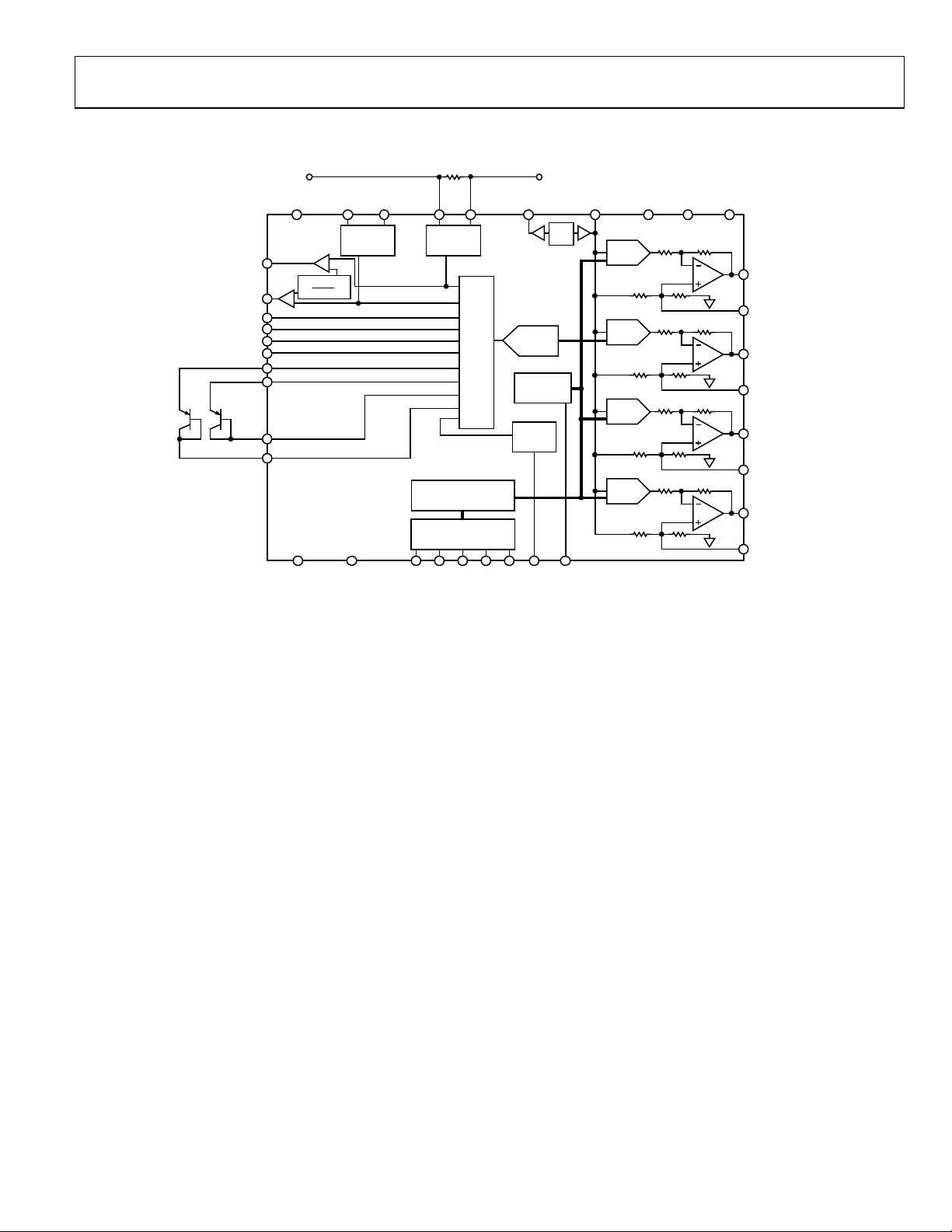
FUNCTIONAL BLOCK DIAGRAM
R
SENSE
OVERRANGE
OVERRANGE
T1 T2
I
SENSE
I
SENSE
VIN0
V
IN
V
IN
V
IN
D1+
D2+
D2–
D1–
1
2
3
VPP(1 TO 2)
2
1
AD7294
DV
V
10.41
DD
RS1(+) RS2(+) RS2(–)RS1(–)
HIGH SIDE
CURRENT
SENSE
REF
DGND
(1 TO 2)
HIGH SIDE
CURRENT
SENSE
CONTROL L OGIC
I2C INTERFACE
PROTOCOL
SDA
MUX
AS1AS2SCL
Figure 1.
REF
REF
IN
12-BIT
ADC
REGIS TERS
TEMP
SENSOR
DCAP
AS0
TO LOAD
OUT
ADC
LIMIT
/
2.5V
REF
ALERT/
BUSY
REF
REF
IN
OUT
DAC
AV
/
DD
(1 TO 6)
12-BIT
DAC
100kΩ 200kΩ
12-BIT
DAC
100kΩ 200kΩ
12-BIT
DAC
100kΩ 200kΩ
12-BIT
DAC
100kΩ 200kΩ
AGND
(1 TO 7)
100kΩ 200kΩ
100kΩ 200kΩ
100kΩ 200kΩ
100kΩ 200kΩ
DAC OUT
V+ AB/CD
V
A
OUT
OFFSET IN A
V
B
OUT
OFFSET IN B
V
C
OUT
OFFSET IN C
V
D
OUT
OFFSET IN D
5747-001
Rev. 0 | Page 3 of 44

AD7294
SPECIFICATIONS
DAC SPECIFICATIONS
AVDD = DVDD = 4.5 V to 5.5 V, AGND = DGND = 0 V, internal 2.5 V reference; V
otherwise noted. DAC OUTV+ AB and DAC OUTV+ CD = 4.5 V to 16.5 V, OFFSET IN x is floating, therefore, the DAC output
span = 0 V to 5 V.
Table 1.
Parameter Min Typ Max Unit Test Conditions/Comments
ACCURACY
Resolution 12 Bits
Relative Accuracy (INL) ±1 ±3 LSB
Differential Nonlinearity (DNL) ±0.3 ±1 LSB Guaranteed monotonic
Zero-Scale Error 2.5 8 mV
1
Full-Scale Error of DAC and
15.5
mV DAC OUTV+ = 5.0 V
Output Amplifier
Full-Scale Error of DAC 2 mV DAC OUTV+ = 15.0 V
Offset Error ±8.575 mV Measured in the linear region, TA = −40°C to +105°C
±2 mV Measured in the linear region, TA = 25°C
Offset Error Temperature
±5 ppm/°C
Coefficient
Gain Error ±0.025 ±0.155 % FSR
Gain Temperature Coefficient ±5 ppm/°C
DAC OUTPUT CHARACTERISTICS
Output Voltage Span 0 2 × V
V 0 V to 5 V for a 2.5 V reference
REF
Output Voltage Offset 0 10 V
Offset Input pin range 0 5 V
1.667 5 V
DC Input Impedance
Output Voltage Settling Time
Slew Rate
2
1.1 V/µs
Short-Circuit Current
Load Current
Capacitive Load Stability
DC Output Impedance
2
75 kΩ 100 kΩ to V
2
8 µs
2
2
40 mA Full-scale current shorted to ground
±10 mA Source and/or sink within 200 mV of supply
2
10 nF R
2
1 Ω
REFERENCE
Reference Output Voltage 2.49 2.5 2.51 V ±0.4% maximum @ 25°C, AVDD = DVDD = 4.5 V to 5.5 V
Reference Input Voltage Range 0 AVDD − 2 V
Input Current 100 125 µA V
Input Capacitance
V
Output Impedance
REF
Reference Temperature
2
20 pF
2
25 Ω
10 25 ppm/°C
Coefficient
1
This value indicates that the DAC output amplifiers can output voltages 15.5 mV below the DAC OUTV+ supply. If higher DAC OUTV+ supply voltages are used, the
full-scale error of the DAC is typically 2 mV with no load.
2
Samples are tested during initial release to ensure compliance; they are not subject to production testing.
= 2.7 V to 5.5 V; TA =−40°C to +105°C, unless
DRIVE
The output voltage span can be positioned in the 0 V to
15 V range; if the OFFSET IN x is left floating, the offset
pin = 2/3 × V
= 3 V
OUT
= OFFSET IN x, DAC HIGH-Z = V
OUT
, giving an output of 0 V to 2 × V
REF
− 2 × V
OFFSET
, and 200 kΩ to AGND, see Figure 47
REF
REF
+ V
, DAC HIGH-Z = 0 V
DAC
DRIVE
REF
1/4 to 3/4 change within 1/2 LSB, measured from last
SCL edge
= ∞
L
= 2.5 V
REF
Rev. 0 | Page 4 of 44

AD7294
ADC SPECIFICATIONS
AVDD = DVDD = 4.5 V to 5.5 V, AGND = DGND = 0 V, V
T
= −40°C to +105°C, unless otherwise noted.
A
Table 2.
Parameter Min Typ Max Unit Test Conditions/Comments
DC ACCURACY
Resolution 12 Bits
Integral Nonlinearity (INL)
1
±0.5 ±1 LSB Differential mode
±0.5 ±1.5 LSB Single-ended or pseudo differential mode
Differential Nonlinearity (DNL)1 ±0.5 ±0.99 LSB
Single-Ended Mode
Offset Error ±1 ±7 LSB
Offset Error Match ±0.4 LSB
Gain Error ±0.5 ±2.5 LSB
Gain Error Match ±0.4 LSB
Differential Mode
Positive Gain Error ±3 LSB
Positive Gain Error Match ±0.5 LSB
Zero Code Error ±3 ±10 LSB
Zero Code Error Match ±0.5 LSB
Negative Gain Error ±3 LSB
Negative Gain Error Match ±0.5 LSB
CONVERSION RATE
Conversion Time
Autocycle Update Rate
2
3 s
2
50 s
Throughput Rate 22.22 kSPS f
ANALOG INPUT
Single-Ended Input Range 0
3
0 2 × V
Pseudo Differential Input Range: V
4
− V
IN−
0
IN+
0 2 × V
Fully Differential Input Range: V
IN+
− V
−V
IN−
REF
−2 × V
Input Capacitance
2
30 pF
DC Input Leakage Current ±1 µA
DYNAMIC PERFORMANCE
Signal-to-Noise Ratio (SNR)
1
72.5 73 dB f
71 72 dB
Signal-to-Noise + Distortion (SINAD) Ratio
1
69 71.5 dB f
71 72.5 dB
Total Harmonic Distortion (THD)
1
−81 –74 dB f
−79 –72 dB
Spurious-Free Dynamic Range (SFDR)
1
−91 −84.5 dB f
−93 −85.5
Channel-to-Channel Isolation
2
−90 dB f
= 2.5 V internal or external; V
REF
V
V
+V
+2 × V
REF
REF
V 0 V to 2 × V
REF
REF
0 V to 2 × V
REF
0 V to V
REF
0 V to 2 × V
REF
DRIVE
Differential, single-ended, and pseudo differential
modes
= 400 kHz
SCL
V 0 V to V
0 V to V
= 10 kHz sine wave; differential mode
IN
= 10 kHz sine wave; single-ended and pseudo
f
IN
differential modes
= 10 kHz sine wave; differential mode
IN
= 10 kHz sine wave; single-ended and pseudo
f
IN
differential modes
= 10 kHz sine wave; differential mode
IN
= 10 kHz sine wave; single-ended and pseudo
f
IN
differential modes
= 10 kHz sine wave; differential mode
IN
= 10 kHz sine wave; single-ended and pseudo
f
IN
differential modes
= 10 kHz to 40 kHz
IN
= 2.7 V to 5.5 V; VPP = AVDD to 59.4 V;
mode
REF
mode
REF
mode
REF
mode
REF
mode
REF
mode
REF
Rev. 0 | Page 5 of 44

AD7294
Parameter Min Typ Max Unit Test Conditions/Comments
TEMPERATURE SENSOR—INTERNAL
Operating Range −40 +105 °C
Accuracy ±2 °C Internal temperature sensor, TA = −30°C to +90°C
±2.5 °C Internal temperature sensor, TA = −40°C to +105°C
Resolution 0.25 °C LSB size
Update Rate 5 ms
TEMPERATURE SENSOR—EXTERNAL External transistor is 2N3906
Operating Range −55 +150 °C Limited by external diode
Accuracy ±2 °C TA = T
Resolution 0.25 °C LSB size
Low Level Output Current Source
Medium Level Output Current Source
High Level Output Current Source
Maximum Series Resistance (RS) for
External Diode
Maximum Parallel Capacitance (CP) for
External Diode
2
2
2
8 µA
2
32 µA
2
128 µA
100 Ω For < ±0.5°C additional error, C
1 nF RS = 0, see Figure 29
CURRENT SENSE VPP = AVDD to 59.4 V
VPP Supply Range AVDD 59.4 V
Gain 12.4375 12.5 12.5625
Gain of 12.5 gives a gain error = 0.5% maximum;
delivers ±200 mV range with +2.5 V reference
RS(+)/RS(−) Input Bias Current 25 32 µA
CMRR/PSRR
2
80 dB Inputs shorted to V
Offset Error ±50 ±340 µV
Offset Drift 1 µV/°C
Amplifier Peak-To-Peak Noise
2
400 µV Referred to input
VPP Supply Current 0.18 0.22 mA VPP = 59.4 V
REFERENCE
Reference Output Voltage 2.49 2.51 V ±0.2% maximum at 25°C only
Reference Input Voltage Range 0.1 4.1 V For four uncommitted ADCs
1 AVDD − 2 For current sense
DC Leakage Current ±2 A
V
Output Impedance
REF
Input Capacitance
2
25 Ω
2
20 pF
Reference Temperature Coefficient 10 25 ppm/°C
1
See the section for more details. Terminolo gy
2
Sampled during initial release to ensure compliance, not subject to production testing.
3
V
or V
must remain within GND/VDD.
IN+
IN−
4
V
= 0 V for specified performance. For full input range on V
IN−
, see . Figure 39
IN−
= −40°C to +105°C
DIODE
= 0, see Figure 30
P
PP
Rev. 0 | Page 6 of 44

AD7294
GENERAL SPECIFICATIONS
AVDD = DVDD = 4.5 V to 5.5 V, AGND = DGND = 0 V, V
DAC OUTV+ AB and DAC OUTV+ CD = 4.5 V to 16.5 V; OFFSET IN x is floating, therefore, DAC output span = 0 V to 5 V; T
−40°C to +105°C, unless otherwise noted.
Table 3.
Parameter Min Typ Max Unit Test Conditions/Comments
LOGIC INPUTS
Input High Voltage, VIH 0.7 V
DRIVE
Input Low Voltage, VIL 0.3 V
Input Leakage Current, IIN ±1 µA
Input Hysteresis, V
0.05 V
HYST
Input Capacitance, CIN 8 pF
Glitch Rejection 50 ns
I2C® Address Pins Maximum External
30 pF Tristate input
Capacitance if Floating
DAC HIGH-Z Pin Leakage 10 µA Input with pull-down resistor, VIN = 5.5 V
1 µA Input with pull-down resistor, VIN = 0 V
LOGIC OUTPUTS
SDA, ALERT SDA and ALERT/BUSY are open-drain outputs
Output Low Voltage, VOL 0.4 V I
0.6 V I
Floating-State Leakage Current ±1 µA
Floating-State Output Capacitance 8 pF
I
OVERRANGE I
SENSE
Output High Voltage, VOH V
Output Low Voltage, VOL 0.2 V I
Overrange Setpoint VFS V
POWER REQUIREMENTS
VPP AVDD 59.4 V
AVDD 4.5 5.5 V
V(+) 4.5 16.5 V
DVDD 4.5 5.5 V Tie DVDD to AVDD
V
2.7 5.5 V
DRIVE
IDD Dynamic 5.3 6.5 mA AVDD + DVDD + V
DAC OUTV+ x, IDD 0.6 0.9 mA
Power Dissipation 70 92 mW
Power-Down
IDD 0.5 1 µA For each AVDD and V
DIDD 1 16.5 µA
DAC OUTV+ x, IDD 35 60 µA
Power Dissipation 2.5 mW
= 2.5 V internal or external; V
REF
= 2.7 V to 5.5 V; VPP = AVDD to 59.4 V;
DRIVE
V SDA, SCL only
V SDA, SCL only
DRIVE
V
DRIVE
Input filtering suppresses noise spikes of less
than 50 ns
= 3 mA
SINK
= 6 mA
SINK
OVERRANGE is a push-pull output
SENSE
− 0.2 V I
DRIVE
× 1.2 mV VFS = ±V
FS
= 200 µA for push-pull outputs
SOURCE
= 200 µA for push-pull outputs
SINK
@ midscale output voltage, DAC outputs
unloaded
ADC/12.5
REF
, DAC outputs unloaded
DRIVE
DRIVE
=
A
Rev. 0 | Page 7 of 44
AD7294
T
TIMING CHARACTERISTICS
I2C Serial Interface
AVDD = DVDD = 4.5 V to 5.5 V, AGND = DGND = 0 V, V
DAC OUTV+ AB and DAC OUTV+ CD = 4.5 V to 16.5 V; OFFSET IN x is floating, therefore, DAC output span = 0 V to 5 V; T
−40°C to +105°C, unless otherwise noted.
= 2.5 V internal or external; V
REF
= 2.7 V to 5.5 V; VPP = AVDD to 59.4 V;
DRIVE
=
A
Table 4.
1
Parameter
f
400 kHz max SCL clock frequency
SCL
Limit at T
, T
Unit Description
MIN
MAX
t1 2.5 µs min SCL cycle time
t2 0.6 µs min t
t3 1.3 µs min t
t4 0.6 µs min t
t5 100 ns min t
2
t
0.9 µs max t
6
0 µs min t
t7 0.6 µs min t
t8 0.6 µs min t
t9 1.3 µs min t
, SCL high time
HIGH
, SCL low time
LOW
, start/repeated start condition hold time
HD,STA
, data setup time
SU,DAT
, data hold time
HD,DAT
, data hold time
HD,DAT
, setup time for repeated start
SU,STA
, stop condition setup time
SU,STO
, bus free time between a stop and a start condition
BUF
t10 300 ns max tR, rise time of SCL and SDA when receiving
0 ns min tR, rise time of SCL and SDA when receiving (CMOS compatible)
t11 300 ns max tF, fall time of SDA when transmitting
0 ns min tF, fall time of SDA when receiving (CMOS compatible)
300 ns max tF, fall time of SCL and SDA when receiving
20 + 0.1C
3
ns min t
b
, fall time of SCL and SDA when transmitting
F
Cb 400 pF max Capacitive load for each bus line
1
See Figure 2.
2
A master device must provide a hold time of at least 300 ns for the SDA signal (referred to the V
edge of SCL.
3
Cb is the total capacitance in pF of one bus line. tR and tF are measured between 0.3 DVDD and 0.7 DVDD.
minimum of the SCL signal) to bridge the undefined region of the falling
IH
Timing and Circuit Diagrams
SDA
SCL
t
9
t
4
START
CONDITION
t
3
t
10
t
6
O OUTPUT PIN
Figure 2. I
t
2
C-Compatible Serial Interface Timing Diagram
t
11
2
t
C
L
50pF
5
200µA
200µA
I
OL
I
OH
REPEATED
CONDITION
V
OH
V
OL
t
7
START
(MIN) OR
(MAX)
t
4
t
1
05747-003
t
8
STOP
CONDITIO N
05747-002
Figure 3. Load Circuit for Digital Output
Rev. 0 | Page 8 of 44
AD7294
ABSOLUTE MAXIMUM RATINGS
TA = 25°C, unless otherwise noted.1
Table 5.
Parameter Rating
VPPx to AGND −0.3 V to +70 V
AVDDx to AGND −0.3 V to +7 V
DAC OUTV+ AB to AGND −0.3 V to +17 V
DAC OUTV+ CD to AGND −0.3 V to +17 V
DVDD to DGND −0.3 V to +7 V
V
to OPGND −0.3 V to +7 V
DRIVE
Digital Inputs to OPGND −0.3 V to V
DRIVE
+ 0.3 V
SDA/SCL to OPGND −0.3 V to +7 V
Digital Outputs to OPGND −0.3 V to V
DRIVE
+ 0.3 V
RS(+)/RS(−) to VPPx VPP − 0.3 V to VPP + 0.3 V
REF
/REFIN ADC to AGND −0.3 V to AVDD + 0.3 V
OUT
REF
/REFIN DAC to AGND −0.3 V to AVDD + 0.3 V
OUT
OPGND to AGND −0.3 V to +0.3 V
OPGND to DGND −0.3 V to +0.3 V
AGND to DGND −0.3 V to +0.3 V
V
x to AGND −0.3 V to DAC OUTV(+) + 0.3 V
OUT
Analog Inputs to AGND −0.3 V to AVDD + 0.3 V
Operating Temperature Range
B Version −40°C to +105°C
Storage Temperature Range −65°C to +150°C
Junction Temperature (TJ Max) 150°C
ESD Human Body Model 1 kV
Reflow Soldering Peak
230°C
Temperature
1
Transient currents of up to 100 mA do not cause SCR latch-up.
Stresses above those listed under Absolute Maximum Ratings
may cause permanent damage to the device. This is a stress
rating only; functional operation of the device at these or any
other conditions above those indicated in the operational
section of this specification is not implied. Exposure to absolute
maximum rating conditions for extended periods may affect
device reliability.
To conform with IPC 2221 industrial standards, it is advisable
to use conformal coating on the high voltage pins.
THERMAL RESISTANCE
Table 6. Thermal Resistance
Package Type θJA θ
Unit
JC
64-Lead TQFP 54 16 °C/W
ESD CAUTION
Rev. 0 | Page 9 of 44
AD7294
PIN CONFIGURATION AND FUNCTION DESCRIPTIONS
C
D
A
N
I
F
E
R
/
T
6
7
)
RS2(–)
RS2(+)
AV
AGND1
AGND2
AV
AGND3
/REFIN DAC
OUT
AV
REF
NC = NO CONNECT
)
–
(
2
1
1
P
P
C
S
P
P
N
V
R
V
64 63 62 61 60 59 58 57 56 55 54 53 52 51 50 49
1
NC
NC
DD
DD
D2–
D2+
D1+
D1–
DD
NC
1
2
3
PIN 1
2
INDICATO R
3
4
5
6
7
8
9
10
11
12
13
14
15
16
17 18 19 20 21 22 23 24 25 26 27 28 29 30 31 32
A
A
C
B
N
T
A
N
I
U
D
O
T
N
V
E
G
S
F
T
F
U
O
O
C
A
D
+
D
(
N
1
G
S
C
A
R
N
AD7294
TQFP
TOP VIEW
(Not to Scale)
B
B
B
A
T
N
I
U
+
O
T
V
V
E
T
S
U
F
O
F
C
O
A
D
6
D
D
V
A
4
D
N
G
A
Figure 4. Pin Configuration
U
5
D
P
O
D
D
V
A
4
D
D
V
A
0
N
A
F
N
G
C
E
I
A
V
D
R
C
D
D
C
C
T
C
N
U
I
+
D
O
T
V
N
V
E
T
G
S
U
F
T
O
F
U
C
O
O
A
C
D
A
D
1
2
3
N
N
N
I
I
I
V
V
V
48
DAC HIGH-Z
47
DGND
1 OVERRANGE
I
46
SENSE
2 OVERRANGE
I
45
SENSE
44
DV
DD
43
DGND
42
V
DRIVE
41
OPGND
40
SCL
39
SDA
38
AS0
37
AS1
36
AS2
35
ALERT/BUSY
34
AGND5
33
NC
D
C
D
N
T
N
I
U
O
T
V
E
S
F
F
O
05747-005
Table 7. Pin Function Descriptions
Pin No. Mnemonic Description
2, 61 RS2(−), RS1(−) Connection for External Shunt Resistor.
3, 60 RS2(+), RS1(+) Connection for External Shunt Resistor.
1, 4, 16, 17,
NC No Connection. Do not connect these pins.
32, 33, 59, 64
1 to AVDD6
5, 8, 14, 25,
56, 57
AV
DD
Analog Supply Pins. The operating range is 4.5 V to 5.5 V. These pins provide the supply voltage for
all the analog circuitry on the AD7294. Connect the AV
supply pins are at the same potential. This supply should be decoupled to AGND with one 10 µF
tantalum capacitor and a 0.1 µF ceramic capacitor for each AVDD pin.
6, 7, 13, 24,
34, 55, 58
AGND1 to AGND7
Analog Ground. Ground reference point for all analog circuitry on the AD7294. Refer all analog
input signals and any external reference signal to this AGND voltage. Connect all seven of these
AGND pins to the AGND plane of the system. Note that AGND5 is a DAC ground reference point and
should be used as a star ground for circuitry being driven by the DAC outputs. Ideally, the AGND
and DGND voltages should be at the same potential and must not be more than 0.3 V apart, even
on a transient basis.
9, 12 D2(−), D1(−)
Temperature Sensor Analog Input. These pins are connected to the external temperature sensing
transistor. See Figure 45 and Figure 46.
10, 11 D2(+), D1(+)
Temperature Sensor Analog Input. These pins are connected to the external temperature sensing
transistor. See Figure 45 and Figure 46.
15 REF
/REFIN DAC
OUT
DAC Reference Output/Input Pin. The REF
power-up, the default configuration of this pin is external reference (REF
reference by writing to the power-down register; see Tab le 27. Decoupling capacitors (220 nF
recommended) are connected to this pin to decouple the reference buffer. Provided the output is
buffered, the on-chip reference can be taken from this pin and applied externally to the rest of a
system. A maximum external reference voltage of AV
of the REF
/REFIN DAC pin.
OUT
and DVDD pins together to ensure that all
DD
/REFIN DAC pin is common to all four DAC channels. On
OUT
− 2 V can be supplied to the REF
DD
). Enable the internal
IN
portion
OUT
Rev. 0 | Page 10 of 44

AD7294
Pin No. Mnemonic Description
18, 23, 26, 31
19, 22, 27, 30 V
20, 29
21, 28
35 ALERT/BUSY
When configured as a busy output, this pin becomes active when a conversion is in progress.
38, 37, 36 AS0, AS1, AS2
39 SDA
40 SCL
41 OPGND Dedicated Ground Pin for I2C Interface.
42 V
43, 47 DGND Digital Ground. This pin is the ground for all digital circuitry.
44 DV
46, 45
48 DAC HIGH-Z
49, 50, 51, 52 VIN3 to VIN0
53 REF
54 DCAP
62, 63 VPP1, VPP2
OFFSET IN A to
OFFSET IN D
OUT
A to V
OUT
D
DAC OUT GND AB,
DAC OUT GND CD
DAC OUTV+ AB,
DAC OUTV+ CD
DRIVE
DD
1 OVERRANGE,
I
SENSE
2 OVERRANGE
I
SENSE
/REFIN ADC
OUT
DAC Analog Offset Input Pins. These pins set the desired output range for each DAC channel. The
DACs have an output voltage span of 5 V, which can be shifted from 0 V to 5 V to a maximum output
voltage of 10 V to 15 V by supplying an offset voltage to these pins. These pins can be left floating,
in which case decouple them to AGND with a 100 nF capacitor.
Buffered Analog DAC Outputs for Channel A to Channel D. Each DAC analog output is driven from
an output amplifier that can be offset using the OFFSET IN x pin. The DAC has a maximum output
voltage span of 5 V that can be level shifted to a maximum output voltage level of 15 V. Each output
is capable of sourcing and sinking 10 mA and driving a 10 nF load.
Analog Ground. Analog ground pins for the DAC output amplifiers on V
and V
D, respectively.
OUT
Analog Supply. Analog supply pins for the DAC output amplifiers on V
V
D, respectively. The operating range is 4.5 V to 16.5 V.
OUT
OUT
OUT
A and V
A and V
OUT
B, and V
OUT
B, and V
OUT
C
OUT
C and
Digital Output. Selectable as an alert or busy output function in the configuration register. This is an
open-drain output. An external pull-up resistor is required.
When configured as an alert, this pin acts as an out-of-range indicator and becomes active when
the conversion result violates the DATA
HIGH
or DATA
register values. See the Alert Status Registers
LOW
section.
2
Digital Logic Input. Together, the logic state of these inputs selects a unique I
C address for the
AD7294. See Tab le 34 for details.
Digital Input/Output. Serial bus bidirectional data. This open-drain output requires a pull-up
resistor.
2
C Bus Clock. The data transfer rate in I2C mode is compatible with both 100 kHz and 400 kHz
Serial I
operating modes. This open-drain output requires pull-up resistors.
Logic Power Supply. The voltage supplied at this pin determines at what voltage the interface
operates. Decouple this pin to DGND. The voltage range on this pin is 2.7 V to 5.5 V and may be
different to the voltage level at AV
and DVDD, but should never exceed either by more than 0.3 V.
DD
To set the input and output thresholds, connect this pin to the supply to which the I2C bus is pulled.
Logic Power Supply. The operating range is 4.5 V to 5.5 V. These pins provide the supply voltage for
all the digital circuitry on the AD7294. Connect the AV
and DVDD pins together to ensure that all
DD
supply pins are at the same potential. Decouple this supply to DGND with a10 µF tantalum
capacitor and a 0.1 µF ceramic capacitor.
Fault Comparator Outputs. These pins connect to the high-side current sense amplifiers.
High Impedance Control on DAC Outputs. When this pin is set to a high logic level, it sets the DAC
outputs to the voltage level on the OFFSET IN x pins. This pin has an internal 1 MΩ pull-down
resistor.
Uncommitted ADC Analog Inputs. These pins are programmable as four single-ended channels or
two true differential analog input channel pairs. See Table 1 and Table 13 for more details.
ADC Reference Input/Output Pin. The REF
ADC. Upon power-up, the default configuration of this pin is external reference (REF
/REFIN ADC pin provides the reference source for the
OUT
). Enable the
IN
internal reference by writing to the power-down register; see Table 27. Connect decoupling
capacitors (220 nF recommended) to this pin to decouple the reference buffer. Provided the output
is buffered, the on-chip reference can be taken from this pin and applied externally to the rest of a
system. A maximum external reference voltage of 2.5 V can be supplied to the REF
REF
/REFIN ADC pin.
OUT
portion of the
OUT
External Decoupling Capacitor Input for Internal Temperature Sensor. Decouple this pin to AGND
using a 0.1 F capacitor. In normal operation, the voltage is typically 3.7 V.
Current Sensor Supply Pins. Power supply pins for the high-side current sense amplifiers. Operating
range is from AV
to 59.4 V. Decouple this supply to AGND. See the Current Sense Filtering section.
DD
Rev. 0 | Page 11 of 44
AD7294
TYPICAL PERFORMANCE CHARACTERISTICS
20
8192 POINT FFT
AV
= DVDD = 5V
DD
V
0
= 5V, V
DRIVE
F
SAMPLE
F
= 10kHz, F
IN
–20
SINGLE ENDED
SNR = 71dB, THD = –82dB
–40
RANGE
REF
= 22.22kSPS
SCLK
= 400kHz
20
8192 POINT FFT
AV
= DVDD = 5V
DD
V
0
= 5V, 2V
DRIVE
F
= 22.22kSPS
SAMPLE
F
= 10kHz, F
IN
–20
DIFFERENTIAL
SNR = 73dB, T HD = –82dB
–40
REF
SCLK
RANGE
= 400kHz
–60
AMPLITUDE ( dB)
–80
–100
–120
0 100008000600040002000
FREQUENCY (kHz)
Figure 5. Signal-to-Noise Ratio Single-Ended, V
20
8192 POINT FFT
AV
= DVDD = 5V
DD
V
0
DRIVE
F
SAMPLE
F
= 10kHz, F
IN
–20
SINGLE ENDED
SNR = 72dB, THD = –80dB
–40
–60
AMPLITUDE ( dB)
–80
–100
–120
0 100008000600040002000
= 5V, 2V
REF
= 22.22kSPS
SCLK
RANGE
= 400kHz
FREQUENCY (kHz)
Figure 6. Signal-to-Noise Ratio Single-Ended, 2 × V
20
8192 POINT FFT
AV
= DVDD = 5V
DD
V
0
DRIVE
F
SAMPLE
F
= 10kHz, F
IN
–20
DIFFERENTIAL
SNR = 72dB, THD = –86dB
–40
–60
AMPLITUDE ( dB)
–80
–100
–120
0 100008000600040002000
= 5V, V
RANGE
REF
= 22.22kSPS
SCLK
= 400kHz
FREQUENCY (kHz)
Figure 7. Signal-to-Noise Ratio Differential, V
REF
Range
REF
Range
Range
REF
–60
AMPLITUDE ( dB)
–80
–100
–120
5747-088
5747-089
5747-087
0 100008000600040002000
FREQUENCY (kHz)
Figure 8. Signal-to-Noise Ratio Differential, 2 × V
1.0
0.8
0.6
0.4
0.2
0
INL (LSB)
–0.2
–0.4
–0.6
–0.8
–1.0
256
768
1280
5120
1024
1536
1792
2048
CODE
2304
TA = 25°C
V
DRIVE
V
REF
V
DD
SINGLE-E NDED
2560
Figure 9. ADC INL Single-Ended, V
1.0
TA = 25°C
V
DNL (LSB)
–0.2
–0.4
–0.6
–0.8
–1.0
DRIVE
0.8
V
REF
V
DD
0.6
SINGLE-ENDED
0.4
0.2
0
256
= 5V, V
= 2.5V
= 5V
5120
768
1024
REF
RANGE
1280
1536
1792
2048
CODE
2304
2560
Figure 10. ADC DNL Single-Ended, V
= 5V, V
= 2.5V
= 5V
2816
2816
3072
Range
REF
3072
REF
REF
REF
3328
3328
Range
Range
RANGE
3840
3584
3840
3584
5747-086
4096
05747-077
4096
05747-072
Rev. 0 | Page 12 of 44
AD7294
INL (LSB)
–0.2
–0.4
–0.6
–0.8
–1.0
DNL (LSB)
INL (LSB)
–0.2
–0.4
–0.6
–0.8
–1.0
1.0
0.8
0.6
0.4
0.2
0
256
768
1280
5120
1024
1536
1792
Figure 11. ADC INL Single-Ended, 2 × V
1.0
TA = 25°C
V
0.8
V
V
0.6
SINGLE-ENDED
DRIVE
REF
DD
= 5V
= 5V
= 5V, 2V
REF
RANGE
0.4
0.2
0
–0.2
–0.4
–0.6
–0.8
–1.0
256
768
1280
5120
1024
1536
1792
Figure 12. ADC DNL Single-Ended, 2 × V
1.0
TA = 25°C
V
0.8
V
V
0.6
DIFFERENTIAL
DRIVE
REF
DD
= 5V, V
= 2.5V
= 5V
REF
RANGE
0.4
0.2
0
256
768
1280
5120
1024
1536
1792
Figure 13. ADC INL Differential, V
2048
CODE
2048
CODE
2048
CODE
2304
2304
2304
TA = 25°C
V
= 5V, 2V
DRIVE
V
= 2.5V
REF
V
= 5V
DD
SINGLE-E NDED
2816
2560
3072
REF
2816
2560
3072
REF
2816
2560
3072
Range
REF
REF
3328
3584
Range
3328
3584
Range
3328
3584
RANGE
3840
3840
3840
4096
4096
4096
05747-078
05747-073
05747-075
INL (LSB)
–0.2
–0.4
–0.6
–0.8
–1.0
DNL (LSB)
–0.2
–0.4
–0.6
–0.8
–1.0
DNL (LSB)
–0.2
–0.4
–0.6
–0.8
–1.0
1.0
TA = 25°C
V
0.8
V
V
0.6
DIFFERENTIAL
DRIVE
REF
DD
= 5V
= 5V
= 5V, V
REF
RANGE
0.4
0.2
0
256
768
1280
5120
1024
1536
1792
Figure 14. ADC INL Differential, V
1.0
TA = 25°C
TA = 25°C
V
V
0.8
V
V
V
DIFFERENTIAL
0.6
DIFFERENTIAL
DRIVE
REF
REF
= 5V
DD
DD
= 5V, 2V
= 2.5V
= 2.5V
= 5V
REF
RANGE
0.4
0.2
0
256
768
1280
5120
1024
1536
1792
Figure 15. ADC DNL Differential, 2 × V
1.0
TA = 25°C
V
0.8
V
V
0.6
DIFFERENTIAL
DRIVE
REF
DD
= 5V, 2V
= 5V
= 5V
REF
RANGE
0.4
0.2
0
256
768
1280
5120
1024
1536
1792
Figure 16. ADC DNL Differential, 2 × V
2048
CODE
2048
CODE
2048
CODE
2304
2304
2304
2560
2560
2560
2816
REF
2816
2816
3328
3072
Range
3328
3072
Range
REF
3328
3072
Range
REF
3584
3584
3584
3840
3840
3840
4096
4096
4096
05747-076
05747-070
05747-071
Rev. 0 | Page 13 of 44
AD7294
1.5
1.0
0.5
0
–0.5
INL (LSB)
–1.0
–1.5
–2.0
MAX INL
MIN INL
T
= 25°C
A
= 5V, V
V
DRIVE
= 5V
V
DD
SINGLE-ENDED
2
C MODE 400kHz
I
REF
RANGE
0.6
0.4
0.2
0
DNL (LSB)
–0.2
–0.4
AVDD = DVDD = 5V
= 5V, INTE RNAL REF,
V
DRIVE
OFFSET IN A/B/C/D = FLOATI NG
INL (LSB)
DNL (LS B)
–0.5
–1.0
–1.5
–2.0
–2.5
0.8
0.6
0.4
0.2
0
–0.2
–0.4
–0.6
2.0
1.5
1.0
0.5
0
0654321
REFERENCE VOL TAGE (V)
Figure 17. ADC INL vs. Reference Voltage
MAX DNL
T
V
V
SINGLE-E NDED
2
I
MIN DNL
0654321
REFERENCE VOL TAGE (V)
Figure 18. ADC DNL vs. Reference Voltage
AVDD = DVDD = 5V
= 5V, INTE RNAL REF,
V
DRIVE
OFFSET IN A/B/C/D = FLOATI NG
256
768
1280
1792
5120
1024
1536
2048
CODE
2304
2560
Figure 19. DAC INL
= 25°C
A
= 5V, V
DRIVE
DD
C MODE 400kHz
= 5V
2816
3072
REF
3328
RANGE
3584
3840
4096
–0.6
256
768
1280
1792
2304
2816
3328
5120
1024
1536
2048
2560
5747-093
CODE
3072
3584
3840
4096
05747-080
Figure 20. DAC DNL
20
15
10
5
0
OUTPUT (µV)
–5
–10
–15
–20
5747-094
012345678910
TIME (s)
5747-097
Figure 21. 0.1 Hz to 10 Hz DAC Output Noise (Code 800)
5.0
4.5
4.0
3.5
3.0
2.5
2.0
DAC OUTPUT (V)
1.5
1.0
0.5
0
–5–4–3–2–1012345678910
05747-079
TIME (µs)
64pF
1nF
10nF
5747-084
Figure 22. Settling Time for a ¼ to ¾ Output Voltage Step
Rev. 0 | Page 14 of 44

AD7294
0.8
0.6
0.4
0.2
0
(%)
–0.2
–0.4
–0.6
–0.8
020
TIME (µs)
64pF
1nF
10nF
18161412108642
5747-085
Figure 23. Zoomed in Settling for a ¼ to ¾ Output Voltage Step
1.0
0.9
0.8
0.7
0.6
(V)
0.5
OUT
V
0.4
0.3
0.2
0.1
Figure 24. DAC Sinking Current at Input Code = x000, (V
–0.1
–0.2
–0.3
–0.4
–0.5
– (V+)
OUT
–0.6
V
–0.7
–0.8
–0.9
–1.0
Figure 25. DAC Sourcing Current at Input Code = x000, (V
DAC A
DAC B
DAC C
DAC D
0
043530252015105
0
AVDD = DVDD = 5V
OFFSET IN = FLOATING
DAC OUT V = 15V
V
= 5V, INTERNAL REF
DRIVE
043530252015105
AVDD = DVDD = 5V
OFFSET IN = FLOATING
DAC OUT V = 15V
V
= 5V, INTERNAL REF
DRIVE
SINK CURRENT (mA)
SOURCE CURRENT (mA)
0
5747-090
= 0 V)
OUT
DAC A
DAC B
DAC C
DAC D
0
5747-091
= 0 V)
OUT
100
80
60
40
20
–20
–40
–60
CHANGE IN OUTP UT VOLT AGE (mV)
–80
–100
0
–50 5020 4030100–10–20–30–40
DAC A
DAC B
DAC C
DAC D
AVDD = DVDD = 5V
OFFSET IN = FLOATING
DAC OUT V = 15V
V
DRIVE
LOAD CURRENT (mA)
= 5V, INTERNAL REF
5747-092
Figure 26. DAC Output Voltage vs. Load Current, Input Code = x800
55
50
45
40
35
30
TEMPERATURE READI NG (°C)
25
20
–5 0 5 10 15 20
TIME (S econds)
05747-064
Figure 27. Response of the AD7294 to Thermal Shock Using 2N3906
(2N3906 Placed in a Stirred Oil Bath)
55
EXTERNAL
INTERNAL
AD7294 IN SOCKET ON
200mm × 100mm 2-LAYE R FR-4 PCB
TIME (Seconds)
05747-066
TEMPERATURE ( °C)
50
45
40
35
30
25
–5 0 60555045403530252015105
Figure 28. Response to Thermal Shock from Room Temperature into 50°C
Stirred Oil (Both the AD7294 and the 2N3906 are Placed in a Stirred Oil Bath)
Rev. 0 | Page 15 of 44

AD7294
–
–
0
–0.2
–0.4
–0.6
–0.8
–1.0
–1.2
ERROR (°C)
–1.4
–1.6
–1.8
–2.0
0 0.5 1.0 1.5 2.0 2.5
Figure 29. Temperature Error vs. Capacitor Between D+ and D−
15
CAPACITANCE FROM D+ TO D– (n F)
50
–55
–60
–65
–70
–75
PSRR (dB)
–80
–85
–90
–95
1k 10k 100k 1M 10M
05747-065
Figure 32. I
Without V
50
Power Supply Rejection Ratio vs. Supply Ripple Frequency
SENSE
Supply Decoupling Capacitors for a 500 mV Ripple
PP
FREQUENCY (Hz)
5747-102
10
5
0
–5
ERROR (°C)
–10
–15
–20
0 20 00 4000 6000 8000 10000 12000
SERIES RESI STANCE (Ω)
Figure 30. Temperature Error vs. Series Resistance for 15 Typical Parts
5
0
–5
–10
–15
–20
–25
–30
AMPLITUDE ( dB)
–35
–40
–45
–50
1k 10k 100k 1M 10M 100M
FREQUENCY (Hz)
Figure 31. Frequency Response of the High-Side Current Sensor
on the AD7294
–60
–70
–80
CMRR (dB)
–90
–100
–110
1 100M10M1M100k10k1k10010
05747-062
Figure 33. I
Common-Mode Rejection Ratio vs. Ripple Frequency for a
SENSE
RIPPLE FREQUENCY (Hz)
5747-103
400 mV Peak-To-Peak Ripple
5747-096
Rev. 0 | Page 16 of 44

AD7294
TERMINOLOGY
DAC TERMINOLOGY
Relative Accuracy
For the DAC, relative accuracy or integral nonlinearity (INL) is
a measure of the maximum deviation, in LSBs, from a straight
line passing through the endpoints of the DAC transfer function.
Differential Nonlinearity
Differential nonlinearity (DNL) is the difference between the
measured change and the ideal 1 LSB change between any two
adjacent codes. A specified differential nonlinearity of ±1 LSB
maximum ensures monotonicity. This DAC is guaranteed monotonic by design.
Zero Code Error
Zero code error is a measure of the output error when zero code
(0x0000) is loaded to the DAC register. Ideally, the output
should be 0 V. The zero code error is always positive in the
AD7294 because the output of the DAC cannot go below 0 V.
Zero code error is expressed in mV.
Full-Scale Error
Full-scale error is a measure of the output error when full-scale
code (0xFFFF) is loaded to the DAC register. Ideally, the output
should be V
− 1 LSB. Full-scale error is expressed in mV.
DD
Gain Error
Gain error is a measure of the span error of the DAC. It is the
deviation in slope of the DAC transfer characteristic from ideal,
expressed as a percent of the full-scale range.
Tot a l U n ad ju s te d E rr o r
Total unadjusted error (TUE) is a measure of the output error,
taking all of the various errors into account.
Zero Code Error Drift
Zero code error drift is a measure of the change in zero code
error with a change in temperature. It is expressed in µV/°C.
Gain Error Drift
Gain error drift is a measure of the change in gain error with
changes in temperature. It is expressed in (ppm of full-scale
range)/°C.
ADC TERMINOLOGY
Signal-to-Noise and Distortion Ratio (SINAD)
The measured ratio of signal-to-noise and distortion at the
output of the ADC. The signal is the rms amplitude of the
fundamental. Noise is the sum of all nonfundamental signals
up to half the sampling frequency (f
/2), excluding dc. The
S
ratio is dependent on the number of quantization levels in the
digitization process; the more levels, the smaller the quantization
noise. The theoretical signal-to-noise and distortion ratio for
an ideal N-bit converter with a sine wave input is given by
Signal-to-(Noise + Distortion) = (6.02 N + 1.76) dB
Thus, the SINAD is 74 dB for an ideal 12-bit converter.
Total Harmonic Distortion (THD)
The ratio of the rms sum of harmonics to the fundamental. For
the AD7294, it is defined as
2
2
THD
where V
V
1
, V5, and V6 are the rms amplitudes of the second through
4
log20)dB(
=
is the rms amplitude of the fundamental and V2, V3,
4
3
V
1
VVVVV
++++
6
5
2
2
2
2
sixth harmonics.
Peak Harmonic or Spurious Noise
The ratio of the rms value of the next largest component in the
ADC output spectrum (up to f
/2 and excluding dc) to the rms
S
value of the fundamental. Typically, the value of this specification
is determined by the largest harmonic in the spectrum, but for
ADCs where the harmonics are buried in the noise floor, it is a
noise peak.
Integral Nonlinearity
The maximum deviation from a straight line passing through
the endpoints of the ADC transfer function. The endpoints are
zero scale, a point 1 LSB below the first code transition, and full
scale, a point 1 LSB above the last code transition.
Differential Nonlinearity
The difference between the measured and the ideal 1 LSB
change between any two adjacent codes in the ADC.
Offset Error
The deviation of the first code transition (00…000) to
(00…001) from the ideal—that is, AGND + 1 LSB.
Offset Error Match
The difference in offset error between any two channels.
Gain Error
The deviation of the last code transition (111…110) to
(111…111) from the ideal (that is, REF
− 1 LSB) after the
IN
offset error has been adjusted out.
Gain Error Match
The difference in gain error between any two channels.
Rev. 0 | Page 17 of 44

AD7294
V
/
6
THEORY OF OPERATION
ADC OVERVIEW
The AD7294 provides the user with a 9-channel multiplexer, an
on-chip track-and-hold, and a successive approximation ADC
based around a capacitive DAC. The analog input range for the
part can be selected as a 0 V to V
configured with either single-ended or differential analog inputs.
The AD7294 has an on-chip 2.5 V reference that can be disabled
when an external reference is preferred. If the internal ADC
reference is to be used elsewhere in a system, the output must
first be buffered.
The various monitored and uncommitted input signals are multiplexed into the ADC. The AD7294 has four uncommitted
analog input channels, V
0 to VIN3. These four channels allow
IN
single-ended, differential, and pseudo differential mode
measurements of various system signals.
ADC TRANSFER FUNCTIONS
The designed code transitions occur at successive integer LSB
values (1 LSB, 2 LSB, and so on). In single-ended mode, the
LSB size is V
2 × V
REF
transfer characteristic for the ADC when outputting straight
binary coding is shown in Figure 34.
111. ..111
111.. .110
111. ..00 0
011. ..111
ADC CODE
000...010
000...001
000...000
NOTE
1. V
REF
In differential mode, the LSB size is 2 × V
to V
range is used, and 4 × V
REF
range is used. The ideal transfer characteristic for the ADC when
outputting twos complement coding is shown in Figure 35 (with
the 2 × V
/4096 when the 0 V to V
REF
/4096 when the 0 V to 2 × V
1LSB
0V
IS EITHER V
Figure 34. Single-Ended Transfer Characteristic
range).
REF
REF
OR 2 × V
input or a 2 × V
REF
range is used and
REF
range is used. The ideal
REF
1LSB = V
ANALOG INPUT
.
REF
/4096 when the 0 V to 2 × V
REF
/4096
REF
V
– 1LSB
REF
/4096 when the 0 V
REF
input,
REF
05747-016
REF
1LSB = 2 ×
011. ..111
011...110
000...001
000...000
111.. .111
ADC CODE
100...010
100...001
100...000
+ 1LSB V
REF
Figure 35. Differential Transfer Characteristic with V
REF
– 1LSB
REF
ANALOG INPUT
409
+V
– 1LSB–V
REF
REF
± V
REF
Input Range
5747-017
For VIN0 to VIN3 in single-ended mode, the output code is
straight binary, where
V
= 0 V, D
IN
= x000, VIN = V
OUT
− 1 LSB, and D
REF
OUT
= xFFF
In differential mode, the code is twos complement, where
V
− V
− V
− V
IN−
IN−
IN−
= 0 V, and D
= V
− 1 LSB, and D
REF
= −V
REF
IN+
V
IN+
V
IN+
OUT
, and D
= x00
= x800
OUT
= x7FF
OUT
Channel 5 and Channel 6 (current sensor inputs) are twos
complement, where
V
− V
− V
− V
IN−
IN−
IN−
= 0 mV, and D
= V
/12.5 − 1 LSB, D
REF
= −V
/12.5, D
REF
IN+
V
IN+
V
IN+
OUT
OUT
= x000
OUT
= x800
= x7FF
Channel 7 to Channel 9 (temperature sensor inputs) are twos
complement with the LSB equal to 0.25°C, where
= 0°C, and D
T
IN
T
= +255.75°C, and D
IN
= −256°C, and D
T
IN
OUT
= x000
OUT
= x800
OUT
= x7FF
ANALOG INPUTS
The AD7294 has a total of four analog inputs. Depending on
the configuration register setup, they can be configured as two
single-ended inputs, two pseudo differential channels, or two
fully differential channels. See the Register Setting section for
further details.
Single-Ended Mode
The AD7294 can have four single-ended analog input channels.
In applications where the signal source has high impedance, it is
recommended to buffer the analog input before applying it to the
ADC. The analog input range can be programmed to be either
0 V to V
or 0 V to 2 × V
REF
. In 2 × V
REF
mode, the input is
REF
effectively divided by 2 before the conversion takes place. Note
that the voltage with respect to GND on the ADC analog input
pins cannot exceed AV
DD
.
If the analog input signal to be sampled is bipolar, the internal
reference of the ADC can be used to externally bias up this
Rev. 0 | Page 18 of 44

AD7294
V
signal so that it is correctly formatted for the ADC. Figure 36
shows a typical connection diagram when operating the ADC
in single-ended mode.
+2.5
+1.25V
–1.25V
0V
V
IN
3R
1
ADDITIONAL PINS OMI TTED FO R CLARITY.
R
R
R
0V
OUT
ADC
0.47µF
1
05747-018
V
IN
VIN3
0
REF
AD7294
Figure 36. Single-Ended Mode Connection Diagram
Differential Mode
The AD7294 can have two differential analog input pairs.
Differential signals have some benefits over single-ended
signals, including noise immunity based on the commonmode rejection of the device and improvements in distortion
performance. Figure 37 defines the fully differential analog
input of the AD7294.
p-p
p-p
V
IN+
AD7294
V
IN–
1
05747-019
V
REF
COMMON-MO DE
VOLTAGE
1
ADDITIONAL PINS OMIT TED FOR CL ARITY.
V
REF
Figure 37. Differential Input Definition
The amplitude of the differential signal is the difference
between the signals applied to V
pair (V
IN+
− V
). The resulting converted data is stored in twos
IN−
IN+
and V
in each differential
IN−
complement format in the result register. Simultaneously drive
V
0 and VIN1 by two signals, each of amplitude V
IN
V
, depending on the range chosen), that are 180° out of
REF
phase. Assuming the 0 V to V
of the differential signal is, therefore, −V
peak (2 × V
), regardless of the common mode (VCM).
REF
range is selected, the amplitude
REF
to +V
REF
(or 2 ×
REF
peak-to-
REF
The common mode is the average of the two signals
(V
+ V
IN−
)/2
IN+
The common mode is, therefore, the voltage on which the two
inputs are centered.
This results in the span of each input being V
CM
± V
/2. This
REF
voltage has to be set up externally, and its range varies with the
reference value, V
. As the value of V
REF
increases, the common-
REF
mode range decreases. When driving the inputs with an amplifier,
the actual common-mode range is determined by the output
voltage swing of the amplifier.
The common mode must be in this range to guarantee the
functionality of the AD7294.
When a conversion takes place, the common mode is rejected,
resulting in a virtually noise-free signal of amplitude −V
+V
, corresponding to the digital output codes of −2048 to
REF
REF
to
+2047 in twos complement format.
If the 2 × V
from −2 ×V
V
= V
IN+
range is used, the input signal amplitude extends
REF
(V
REF
REF
= 0 V, V
IN+
).
IN−
= V
) to +2 × V
REF
REF
(V
IN−
= 0 V,
Driving Differential Inputs
The differential modes available on VIN0 to VIN3 in Tabl e 13
require that V
IN+
and V
be driven simultaneously with two
IN−
equal signals that are 180° out of phase. The common mode on
which the analog input is centered must be set up externally. The
common-mode range is determined by V
, the power supply,
REF
and the particular amplifier used to drive the analog inputs.
Differential modes of operation with either an ac or dc input
provide the best THD performance over a wide frequency
range. Because not all applications have a signal preconditioned
for differential operation, there is often a need to perform a singleended-to-differential conversion.
Using an Op Amp Pair
An op amp pair can be used to directly couple a differential signal
to one of the analog input pairs of the AD7294. The circuit configurations illustrated in Figure 38 show how a dual op amp can
be used to convert a single-ended bipolar signal into a differential
unipolar input signal.
The voltage applied to Point A sets up the common-mode voltage.
As shown in Figure 38, Point A connects to the reference, but any
value in the common-mode range can be the input at Point A to
set up the common mode. The AD8022 is a suitable dual op amp
that can be used in this configuration to provide differential
drive to the AD7294.
Care is required when choosing the op amp because the selection
depends on the required power supply and system performance
objectives. The driver circuits in Figure 38 are optimized for dc
coupling applications requiring best distortion performance.
The differential op amp driver circuit shown in Figure 38 is
configured to convert and level shift a single-ended, ground
referenced (bipolar) signal to a differential signal centered at the
V
level of the ADC.
REF
Rev. 0 | Page 19 of 44

AD7294
GND
2 × V
REF
p-p
440Ω
220kΩ
20kΩ
220Ω
V+
27Ω
V–
220Ω
220Ω
V+
27Ω
A
V–
10kΩ
1
ADDITIONAL PINS O MITTED FO R CLARITY.
3.75V
2.5V
1.25V
3.75V
2.5V
1.25V
AD7294
ADC
OUT
0.47µF
1
V
IN+
REF
V
IN–
Figure 38. Dual Op Amp Circuit to Convert a Single-Ended Bipolar Signal
into a Differential Unipolar Signal
Pseudo Differential Mode
The four uncommitted analog input channels can be configured
as two pseudo differential pairs. Uncommitted input, V
V
1, are a pseudo differential pair, as are VIN2 and VIN3. In this
IN
mode, V
maximum amplitude of V
is connected to the signal source, which can have a
IN+
(or 2 × V
REF
, depending on the
REF
0 and
IN
range chosen) to make use of the full dynamic range of the part.
A dc input is applied to V
provides an offset from ground or a pseudo ground for the V
input. Which channel is V
. The voltage applied to this input
IN−
is determined by the ADC channel
IN+
IN+
allocation. The differential mode must be selected to operate in the
pseudo differential mode. The resulting converted pseudo differential data is stored in twos complement format in the result register.
The governing equation for the pseudo differential mode, for
V
0 is
IN
V
where V
OUT
= 2(V
IN+
− V
IN+
IN−
) − V
REF_ADC
is the single-ended signal and V
is a dc voltage.
IN−
The benefit of pseudo differential inputs is that they separate
the analog input signal ground from the ADC ground, allowing
dc common-mode voltages to be cancelled. The typical voltage
range for V
while in pseudo differential mode is shown in
IN−
Figure 39; Figure 40 shows a connection diagram for pseudo
differential mode.
2.0
1.5
1.0
(V)
IN–
V
0.5
0
–0.5
054321
Figure 39. V
Input Range vs. V
IN−
V
(V)
REF
in Pseudo Differential Mode
REF
AVDD = DVDD = 5V
V
= 5V
DRIVE
6
05747-095
Rev. 0 | Page 20 of 44
V
REF
p-p
V
IN+
V
DC INPUT
VOLTAGE
1
ADDITIONAL PINS OMITTED FO R CLARITY.
REF
IN–
OUT
/REFIN ADC
AD7294
0.47µF
1
05747-026
Figure 40. Pseudo Differential Mode Connection Diagram
05747-023
CURRENT SENSOR
Two bidirectional high-side current sense amplifiers are
provided that can accurately amplify differential current shunt
voltages in the presence of high common-mode voltages from
AV
up to 59.4 V. Each amplifier can accept a ±200 mV
DD
differential input. Both current sense amplifiers have a fixed
gain of 12.5 and utilize an internal 2.5 V reference.
An analog comparator is also provided with each amplifier for
fault detection. The threshold is defined as
1.2 × Full-Scale Voltage Range
When this limit is reached, the output is latched onto a
dedicated pin. This output remains high until the latch is
cleared by writing to the appropriate register.
I
AVDD TO 54.5V
V
PP
AD7294
100kΩ
R
RS(+)
R1
40kΩ
Q1 Q2
R3
SENSE
A1
A1
RS(–)
R2
40kΩ
LOAD
R4
100kΩ
V
OUT
A2
TO MUX
05747-029
Figure 41. High-Side Current Sense
The AD7294 current sense comprises two main blocks: a
differential and an instrumentation amplifier. A load current
flowing through the external shunt resistor produces a voltage
at the input terminals of the AD7294. Resistors R1 and R2
connect the input terminals to the differential amplifier (A1).
A1 nulls the voltage appearing across its own input terminals
by adjusting the current through R1 and R2 with Transistor Q1
and Transistor Q2. Common-mode feedback maintains the sum
of these currents at approximately 50 A. When the input signal
to the AD7294 is zero, the currents in R1 and R2 are equal. When
the differential signal is nonzero, the current increases through
one of the resistors and decreases in the other. The current difference is proportional to the size and polarity of the input signal.
The differential currents through Q1 and Q2 are converted into
a differential voltage by R3 and R4. A2 is configured as an instrumentation amplifier, buffering this voltage and providing additional

AD7294
V
gain. Therefore, for an input voltage of ±200 mV at the pins, an
output span of ±2.5 V is generated.
The current sensors on the AD7294 are designed to remove any
flicker noise and offset present in the sensed signal. This is
achieved by implementing a chopping technique that is transparent to the user. The V
signal is first converted by the AD7294,
SENSE
the analog inputs to the amplifiers are then swapped, and the
differential voltage is once again converted by the AD7294. The
two conversion results enable the digital removal of any offset
or noise. Switches on the amplifier inputs enable this chopping
technique to be implemented. This process requires 6 s in total
to return a final result.
Choosing R
SENSE
The resistor values used in conjunction with the current sense
amplifiers on the AD7294 are determined by the specific application requirements in terms of voltage, current, and power.
Small resistors minimize power dissipation, have low inductance
to prevent any induced voltage spikes, and have good tolerance,
which reduce current variations. The final values chosen are a
compromise between low power dissipation and good accuracy.
Low value resistors have less power dissipated in them, but higher
value resistors may be required to utilize the full input range of
the ADC, thus achieving maximum SNR performance.
When the sense current is known, the voltage range of the
AD7294 current sensor (200 mV) is divided by the maximum
sense current to yield a suitable shunt value. If the power dissipation in the shunt resistor is too large, the shunt resistor can be
reduced, in which case, less of the ADC input range is used.
Using less of the ADC input range results in conversion results,
which are more susceptible to noise and offset errors because
offset errors are fixed and are thus more significant when
smaller input ranges are used.
R
must be able to dissipate the I2R losses. If the power dissi-
SENSE
pation rating of the resistor is exceeded, its value may drift or
the resistor may be damaged resulting in an open circuit. This
can result in a differential voltage across the terminals of the
AD7294 in excess of the absolute maximum ratings. Additional
protection is afforded to the current sensors on the AD7294 by
the recommended current limiting resistors, RF1 and RF2, as
illustrated in Figure 42. The AD7294 can handle a maximum
continuous current of 30 mA; thus, an RF2 of 1 kΩ provides
adequate protection for the AD7294.
If I
has a large high frequency component, take care to
SENSE
choose a resistor with low inductance. Low inductance metal
film resistors are best suited for these applications.
Current Sense Filtering
In some applications, it may be desirable to use external
filtering to reduce the input bandwidth of the amplifier (see
Figure 42). The −3 dB differential bandwidth of this filter is
equal to
BW
= 1/(4πRC)
DM
Note that the maximum series resistance on the RS(+) and
RS(−) inputs (as shown in Figure 41) is limited to a maximum
of 1 k due to back-to-back ESD protection diodes from RS(+)
and RS(−) to V
. Also, note that if RF1 and RF2 are in series
PP
with R1 and R2 (shown in Figure 41), it affects the gain of the
amplifier. Any mismatch between RF1 and RF2 can introduce
offset error.
PP
10nF
V
PP
AD7294
Figure 42. Current Sense Filtering (RS
R
RF1 RF2
Can Be Either RS1 or RS2)
X
SENSE
CF
I
LOAD
RSx(–)RSx(+)
5747-098
For certain RF applications, the optimum value for RF1 and
RF2 is 1 k whereas CF1 can range from 1 F to 10 F. CF2 is a
decoupling capacitor for the V
supply. Its value is application
PP
dependant, but for initial evaluation, values in the range of 1 nF
to 100 nF are recommended.
Kelvin Sense Resistor Connection
When using a low value sense resistor for high current
measurement, the problem of parasitic series resistance can
arise. The lead resistance can be a substantial fraction of the
rated resistance, making the total resistance a function of lead
length. Avoid this problem by using a Kelvin sense connection.
This type of connection separates the current path through the
resistor and the voltage drop across the resistor. Figure 43 shows
the correct way to connect the sense resistor between the RS(+)
and RS(−) pins of the AD7294.
SENSE RESISTOR
CURRENT
FLOW FROM
SUPPLY
KELVIN
SENSE
TRACES
RSX(+) RSX(–)
AD7294
Figure 43. Kelvin Sense Connections (RSX Can Be Either RS1 or RS2)
CURRENT
FLOW TO
LOAD
05747-031
ANALOG COMPARATOR LOOP
The AD7294 contains two setpoint comparators that are used
for independent analog control. This circuitry enables users
to quickly detect if the sensed voltage across the shunt has
Rev. 0 | Page 21 of 44

AD7294
V
2
2
increased about the preset (V
I
OVERRANGE pin is set to a high logic level enabling
SENSE
appropriate action to be taken to prevent any damage to the
external circuitry.
The setpoint threshold level is fixed internally in the AD7294,
and the current sense amplifier saturates above this level. The
comparator also triggers if a voltage of less than AV
to the R
or VPP pin.
SENSE
TEMPERATURE SENSOR
The AD7294 contains one local and two remote temperature
sensors. The temperature sensors continuously monitor the
three temperature inputs and new readings are automatically
available every 5 ms.
The on-chip, band gap temperature sensor measures the temperature of the system. Diodes are used in conjunction with the two
remote temperature sensors to monitor the temperature of other
critical board components.
4 × I
16 × I I I-BIAS
D2+
D1+
T1 T2
REMOTE
SENSING
TRANSISTORS
The temperature sensor module on the AD7294 is based on the
three current principle (see Figure 44), where three currents are
passed through a diode and the forward voltage drop is measured
at each diode, allowing the temperature to be calculated free of
errors caused by series resistance.
Each input integrates, in turn, over a period of several hundred
microseconds. This takes place continuously in the background,
leaving the user free to perform conversions on the other channels.
When integration is complete, a signal passes to the control logic
to initiate a conversion automatically. If the ADC is in command
mode, the temperature conversion is performed as soon as the
next conversion is completed. In autocycle mode, the conversion
is inserted into an appropriate place in the current sequence; see
the Register Setting section for further details. If the ADC is
idle, the conversion takes place immediately.
Three registers store the result of the last conversion on each
temperature channel; these can be read at any time. In addition,
in command mode, one or both of the two external channel
registers can be read out as part of the output sequence.
D1–
D2–
Figure 44. Internal and Remote Temperature Sensors
MUX
AD7294
× 1.2)/12.5. If this occurs, the
REF
is applied
DD
DD
TO ADC
LPF
MUX
LIMIT
REGISTERS
TEMP
SENSOR
CAP
f
= 65kHz
C
BIAS DIODE
ALERT
Remote Sensing Diode
The AD7294 is designed to work with discrete transistors,
2N3904 and 2N3906. If an alternative transistor is used, the
AD7294 operates as specified provided the following conditions
are adhered to.
Ideality Factor
The ideality factor, nf, of the transistor is a measure of the
deviation of the thermal diode from ideal behavior. The
AD7294 is trimmed for an n
value of 1.008. Use the following
f
equation to calculate the error introduced at a Temperature T
(°C) when using a transistor whose n
T = (n
− 1.008) × (273.15 K + T)
f
does not equal 1.008:
f
To factor this in, the user can write the ∆T value to the offset
register. The AD7294 automatically adds it to, or subtracts it
from, the temperature measurement.
Base Emitter Voltage
The AD7294 operates as specified provided that the baseemitter voltage is greater than 0.25 V at 8 µA at the highest
operating temperature, and less than 0.95 V at 128 µA for the
lowest operating temperature.
Base Resistance
The base resistance should be less than 100 Ω.
hFE Vari ati o n
A transistor with small variation in hFE (approximately 50 to
150) should be used. Small variation in h
control of the V
characteristics.
BE
indicates tight
FE
For RF applications, the use of high Q capacitors functioning as
05747-032
a filter protects the integrity of the measurement. These
capacitors, such as Johanson Technology 10 pF high Q
capacitors: Reference Code 500R07S100JV4T, should be
connected between the base and the emitter, as close to the
external device as possible. However, large capacitances affect
the accuracy of the temperature measurement; thus, the
recommended maximum capacitor value is 100 pF. In most
cases, a capacitor is not required; the selection of any capacitor
is dependent on the noise frequency level.
AD7294
N3904
NPN
Figure 45. Measuring Temperature Using an NPN Transistor
N3906
PNP
Figure 46. Measuring Temperature Using a PNP Transistor
10pF
10pF
D+
D–
AD7294
D+
D–
5747-099
05747-100
Rev. 0 | Page 22 of 44

AD7294
V
Series Resistance Cancellation
= 3V
= 3V
DAC
R
R
R
R
R
Figure 48. Resistor String Structure
. The second amplifier, A2, is
REF
OFFSET
OFFSET
=
⎡
V
⎢
⎣
− 2V
+ 2(V
REF
DAC
− V
DAC
D
⎛
×
⎜
n
2
⎝
)
REF
⎤
⎞
⎟
⎥
⎠
⎦
TO OUTPUT
AMPLIFIER
5747-028
The AD7294 has been designed to automatically cancel out the
effect of parasitic, base, and collector resistance on the temperature reading. This gives a more accurate result, without the need
for any user characterization of the parasitic resistance. The
AD7294 can compensate for up to 100 in a process that is
transparent to the user.
DAC OPERATION
The AD7294 contains four 12-bit DACs that provide digital
control with 12 bits of resolution with a 2.5 V internal reference.
The DAC core is a thin film 12-bit string DAC with a 5 V output
span and an output buffer that can drive the high voltage output
stage. The DAC has a span of 0 V to 5 V with a 2.5 V reference
input. The output range of the DAC, which is controlled by the
offset input, can be positioned from 0 V to 15 V. Figure 47 is a
block diagram of the DAC architecture.
5
DAC
HIGH-Z
R1
R1
100kΩR2200kΩ
REF
REF
IN
OUT
DAC
/
12-BIT
DAC
I
DATA INPUTS
EXTERNAL
REFERENCE
CAPACIT OR
A1
V
DAC
2
C
100kΩR2200kΩ
Figure 47. DAC Architecture
Resistor String
The resistor string structure is shown in Figure 48. It consists of
n
a string of 2
resistors, each of Value R. The code loaded to the
DAC register determines at which node on the string the voltage
is tapped off to be fed into the output amplifier. The voltage is
tapped off by closing one of the switches connecting the string
to the amplifier. This architecture is inherently monotonic,
voltage out, and low glitch. It is also linear because all of the
resistors are of equal value.
15V
A2
AGND
DAC OUT V+ xx
(POWER DOWN
REGISTER = 0)
OFFSET IN x
5747-101
Output Amplifier
Referring to Figure 47, the purpose of A1 is to buffer the DAC
output range from 0 V to V
configured such that when an offset is applied to OFFSET IN x,
its output voltage is three times the offset voltage minus twice
the DAC voltage.
V
OUT
The DAC word is digitally inverted on-chip such that
V
OUT
and V
where:
V
is the output of the DAC before digital inversion.
DAC
D is the decimal equivalent of the binary code that is loaded to the
DAC register.
n is the bit resolution of the DAC.
An example of the offset function is given in Table 8 .
Table 8. Offset Voltage Function Example
Offset
Voltage
with 0x000 V
V
OUT
with 0xFFF
OUT
1.67 V 0 V 5 V − 1 LSB
3.33 V 5 V 10 V − 1 LSB
5.00 V 10 V 15 V − 1 LSB
The user has the option of leaving the offset pin open, in which
case the voltage on the noninverting input of Op Amp A2 is set
by the resistor divider, giving
V
= 2V
OUT
Rev. 0 | Page 23 of 44
DAC

AD7294
This generates the 5 V output span from a 2.5 V reference.
Digitally inverting the DAC allows the circuit to operate as a
generic DAC when no offset is applied. If the offset pin is not
being driven, it is best practice to place a 100 nF capacitor
between the pin and ground to improve both the settling time
and the noise performance of the DAC.
Note that a significant amount of power can be dissipated in the
DAC outputs. A thermal shutdown circuit sets the DAC outputs
to high impedance if a die temperature of >150°C is measured
by the internal temperature sensor. This also sets the overtemperature alert bit in Alert Register C, see the Alerts and Limits
Theory section. Note that this feature is disabled when the
temperature sensor powers down.
High Impedance Input Pin
When the high impedance pin (DAC HIGH-Z pin) is taken
high by the user (see Figure 47), the voltage on the offset pin
appears on the DAC output voltage pin. Essentially, the Internal
Amplifier A2 acts as a voltage follower. This feature allows a fast
change in the output when a fault occurs.
ADC AND DAC REFERENCE
The AD7294 has two independent internal high performance
2.5 V references, one for the ADCs and the other for the four
on-chip DACs. If the application requires an external reference,
it can be applied to the REF
REF
/REFIN ADC pin. The internal reference should be buffered
OUT
before being used by external circuitry. Decouple both the REF
REF
DAC pin and the REF
IN
220 nF capacitor. On power-up, the AD7294 is configured for
use with an external reference. To enable the internal references,
write a zero to both the D4 and D5 bits in the power-down
/REFIN DAC pin and/or to the
OUT
/REFIN ADC pin to AGND using a
OUT
OUT
/
register (see the Register Setting section for more details). Both
the ADC and DAC references require a minimum of 60 s to
power up and settle to a 12-bit performance when a 220 nF
decoupling capacitor is used.
The AD7294 can also operate with an external reference.
Suitable reference sources for the AD7294 include AD780,
AD1582, ADR431, REF193, and ADR391. In addition, choosing
a reference with an output trim adjustment, such as the ADR441,
allows a system designer to trim system errors by setting a
reference voltage to a voltage other than the nominal.
Long-term drift is a measure of how much the reference drifts
over time. A reference with a low long-term drift specification
ensures that the overall solution remains stable during its entire
lifetime. If an external reference is used, select a low temperature
coefficient specification to reduce the temperature dependence
of the system output voltage on ambient conditions.
V
FEATURE
DRIVE
The AD7294 also has a V
2
which the I
C interface operates. The V
the supply to which the I
feature to control the voltage at
DRIVE
pin is connected to
2
C bus is pulled. This pin sets the input
DRIVE
and output threshold levels for the digital logic pins and the
I
OVERRANGE pins. The V
SENSE
feature allows the AD7294
DRIVE
to easily interface to both 3 V and 5 V processors. For example,
if the AD7294 is operated with a V
of 5 V, the V
DD
DRIVE
pin can
be powered from a 3 V supply, allowing a large dynamic range
with low voltage digital processors. Thus, the AD7294 can be
used with the 2 × V
input range with a VDD of 5 V, yet remains
REF
capable of interfacing to 3 V digital parts. Decouple this pin to
DGND with a 100 nF and a 1 F capacitor.
Rev. 0 | Page 24 of 44

AD7294
REGISTER SETTING
The AD7294 contains internal registers (see Figure 49) that
store conversion results, high and low conversion limits, and
information to configure and control the device.
COMMAND
REGISTER
RESULT
REGISTER
DAC
REGISTERS
T
RESULT
SENSE
REGISTERS × 3
ALERT
REGISTERS × 3
CHANNEL
ADDRESS
POINTER
REGISTER
SERIAL BUS INTERFACE
SEQUENCE
REGISTER
CONFIGURATIO N
REGISTE R
POWER-DOWN
REGISTER
DATA
/
HIGH
DATA
LOW
REGISTERS × 18
HYSTERESIS
REGISTER
OFFSET
T
SENSE
REGISTERS × 2
DATA
SDA
SCL
05747-039
Figure 49. AD7294 Register Structure
Each data register has an address to which the address pointer
register points when communicating with it. The command
register is the only register that is a write-only register; the rest
are read/write registers.
ADDRESS POINTER REGISTER
The address pointer register is an 8-bit register, in which the
6 LSBs are used as pointer bits to store an address that points
to one of the AD7294 data registers, see Tabl e 9.
Table 9. AD7294 Register Address
Address in Hex Registers (R is Read/W is Write)
00 Command Register (W)
01 Result Register (R)/DACA Value (W )
02 T
03 T
04 T
1 Result (R)/DACB Value (W)
SENSE
2 Result (R)/DACC Value (W)
SENSE
INT Result (R)/DACD Value (W )
SENSE
05 Alert Register A (R/W)
06 Alert Register B (R/W)
07 Alert Register C (R/W)
08 Channel Sequence Register (R/W)
09 Configuration Register (R/W)
0A Power-Down Register (R/W)
0B DATA
0C DATA
Register VIN0 (R/W)
LOW
Register VIN0 (R/W)
HIGH
0D Hysteresis Register VIN0 (R/W)
0E DATA
0F DATA
Register VIN1 (R/W)
LOW
Register VIN1 (R/W)
HIGH
10 Hysteresis Register VIN1 (R/W)
11 DATA
12 DATA
Register, VIN2 (R/W)
LOW
Register VIN2 (R/W)
HIGH
13 Hysteresis Register VIN2 (R/W)
14 DATA
15 DATA
Register VIN3 (R/W)
LOW
Register VIN3 (R/W)
HIGH
16 Hysteresis Register VIN3 (R/W)
17 DATA
18 DATA
19 Hysteresis Register I
1A DATA
1B DATA
1C Hysteresis Register I
1D DATA
1E DATA
1F Hysteresis Register T
20 DATA
21 DATA
22 Hysteresis Register T
23 DATA
24 DATA
25 Hysteresis Register T
26 T
27 T
Register I
LOW
Register I
HIGH
Register I
LOW
Register I
HIGH
Register T
LOW
Register T
HIGH
Register T
LOW
Register T
HIGH
Register T
LOW
Register T
HIGH
1 Offset Register (R/W)
SENSE
2 Offset Register (R/W)
SENSE
SENSE
SENSE
SENSE
SENSE
SENSE
SENSE
SENSE
SENSE
SENSE
SENSE
SENSE
SENSE
SENSE
SENSE
SENSE
1 (R/W)
1 (R/W)
2 (R/W)
2 (R/W)
1 (R/W)
2 (R/W)
1 (R/W)
1 (R/W)
1 (R/W)
2 (R/W)
2 (R/W)
2 (R/W)
INT (R/W)
INT (R/W)
INT (R/W)
40 Factory Test Mode
41 Factory Test Mode
Rev. 0 | Page 25 of 44

AD7294
COMMAND REGISTER (0x00)
Writing in the command register puts the part into command
mode. When in command mode, the part cycles through the
selected channels from LSB (D0) to MSB (D7) on each subsequent read (see Tab le 1 0 ). A channel is selected for conversion
if a one is written to the desired bit in the command register. On
power-up, all bits in the command register are set to zero. If the
external T
byte, it is not actually requesting a conversion. The result of the
last automatic conversion is output as part of the sequence (see
the Modes of Operation section).
The command mode can be used when the autocycle mode is
enabled (see the Autoc ycle Mode for more details). In this case,
the automatic conversion sequence pauses while the command
mode is active and resumes when the command mode is exited
(either by a stop bit or after 5 ms of idle time).
channels are selected in the command register
SENSE
RESULT REGISTER (0x01)
The result register is a 16-bit read-only register. The conversion
results for the four uncommitted ADC inputs and the two I
channels are stored in the result register for reading. Bit D14 to
Bit D12 are the channel allocation bits, each of which identifies
the ADC channel that corresponds to the subsequent result (see
the ADC Channel Allocation section for more details). Bit D11
to Bit D0 contain the most recent ADC result. D15 is reserved
as an alert_flag bit. Tabl e 11 lists the contents of the first byte
that is read from the AD7294 results register; Ta b l e 1 2 lists the
contents of the second byte read.
SENSE
Table 10. Command Register
1
MSB LSB
Bits D7 D6 D5 D4 D3 D2 D1 D0
Channel
Read out
last result
from T
SENSE
2
Read out
last result
from T
SENSE
2 I
SENSE
1
1 VIN3 (S.E.)
SENSE
or
VIN3 − VIN2 (DIFF)
VIN2 (S.E.)
or
VIN2 − VIN3 (DIFF)
VIN1(S.E.)
or
VIN1 − VIN0
VIN0 (S.E.)
or
0 − VIN1 (DIFF)
V
IN
I
(DIFF)
1
S.E. indicates single-ended and DIFF indicates differential.
Table 11. Result Register (First Read)
MSB LSB
D15 D14 D13 D12 D11 D10 D9 D8
Alert_Flag CH
CH
ID2
CH
ID1
B11 B10 B9 B8
ID0
Table 12. Result Register (Second Read)
MSB LSB
D7 D6 D5 D4 D3 D2 D1 D0
B7 B6 B5 B4 B3 B2 B1 B0
Rev. 0 | Page 26 of 44

AD7294
ADC Channel Allocation
The three channel address bits indicate which channel the result
in the result register represents. Ta b l e 1 3 details the channel ID bits
(S.E. indicates single-ended and DIFF indicates differential).
Table 14. T
Register (First Read)
SENSE
MSB LSB
D15 D14 D13 D12 D11 D10 D9 D8
Alert_Flag CH
ID2
CH
ID1
CH
B11 B10 B9 B8
ID0
Table 13. ADC Channel Allocation
Channel ID
Functio n
VIN0 (S.E.) or
0 − VIN1 (DIFF)
V
IN
VIN1 (S.E.) or
1 − VIN0 (DIFF)
V
IN
VIN2 (S.E.) or
V
2 − VIN3 (DIFF)
IN
VIN3 (S.E.) or
3 − VIN2 (DIFF)
V
IN
I
1 1 0 0
SENSE
I
2 1 0 1
SENSE
T
1 1 1 0
SENSE
T
2 1 1 1
SENSE
T
1, T
SENSE
Register T
SENSE
1 and Register T
SENSE
CH
CH
ID2
CH
ID1
ID0
0 0 0
0 0 1
0 1 0
0 1 1
2 RESULT REGISTERS (0x02 AND 0x03)
2 are 16-bit read only registers.
SENSE
The MSB, D15 is the alert_flag bit whereas Bit D14 to Bit D12
contain the three ADC channel allocation bits. D11 is reserved
for flagging diode open circuits. The temperature reading from
the ADC is stored in an 11-bit twos complement format, D10 to
D0 (see Tabl e 14 and Tab le 1 5 ). Conversions take place approximately every 5 ms.
Table 15. Register (Second Read)
MSB LSB
D7 D6 D5 D4 D3 D2 D1 D0
B7 B6 B5 B4 B3 B2 B1 B0
T
INT RESULT REGISTER (0x04)
SENSE
The T
INT register is a 16-bit read-only register used to
SENSE
store the ADC data generated from the internal temperature
sensor. Similar to the T
SENSE
1 and T
2 result registers, this
SENSE
register stores the temperature readings from the ADC in an
11-bit twos complement format, D10 to D0, and uses the MSB
as a general alert flag. Bits[ D14:D11] are not used and are set to
zero. Conversions take place approximately every 5 ms. The
temperature data format in Ta bl e 16 also applies to the internal
temperature sensor data.
Temperature Value Format
The temperature reading from the ADC is stored in an 11-bit
twos complement format, D10 to D0, to accommodate both
positive and negative temperature measurements. The temperature data format is provided in Ta bl e 16.
Table 16. T
Data Format
SENSE
Input D10 (MSB) D9 D8 D7 D6 D5 D4 D3 D2 D1 D0 (LSB)
Value (°C)
−256 +128 +64 +32 +16 +8 +4 +2 +1 +0.5 +0.25
Rev. 0 | Page 27 of 44

AD7294
DACA, DACB, DACC, DACD, REGISTER (0x01 TO 0x04)
Writing to these register addresses sets the DACA, DACB, DACC,
and DAC
the write result register are the data bits sent to DAC
to Bit D12 are ignored.
Table 17. DAC Register (First Write)
MSB LSB
D15 D14 D13 D12 D11 D10 D9 D8
X X X X B11 B10 B9 B8
1
X is don’t care.
Table 18. DAC Register (Second Write)
MSB LSB
D7 D6 D5 D4 D3 D2 D1 D0
B7 B6 B5 B4 B3 B2 B1 B0
output voltage codes, respectively. Bits[D11:D0] in
D
. Bit D15
A
1
ALERT STATUS REGISTER A (0x05), REGISTER B (0x06), AND REGISTER C (0x07)
The alert status registers (A, B, and C) are 8-bit read/write
registers that provide information on an alert event. If a
conversion results in activating the ALERT/BUSY pin or the
alert_flag bit in the result register or T
registers, the alert
SENSE
status register can be read to gain further information. To clear
the full content of any one of the alert registers, write a code of
FF (all ones) to the relevant registers. Alternatively, the user can
write to the respective alert bit in the selected alert register to
clear the alert associated with that bit. The entire contents of all
the alert status registers can be cleared by writing a 1 to Bit D1
and Bit D2 in the configuration register, as shown in Tabl e 24 .
However, this operation then enables the ALERT/BUSY pin for
subsequent conversions. See the Alerts and Limits Theory
section for more details.
CHANNEL SEQUENCE REGISTER (0x08)
The channel sequence register is an 8-bit read/write register that
allows the user to sequence the ADC conversions to be
performed in autocycle mode. Ta bl e 2 2 shows the content of the
channel sequence register. See the Modes of Operation section
for more information.
Table 19. Alert Status Register A
Alert Bit D7 D6 D5 D4 D3 D2 D1 D0
Functio n
3
V
IN
high alert
VIN3
low alert
VIN2
high alert
VIN2
low alert
VIN1
high alert
VIN1
low alert
VIN0
high alert
VIN0
low alert
Table 20. Alert Status Register B
Alert Bit D7 D6 D5 D4 D3 D2 D1 D0
Functio n
Reserved Reserved
2
I
SENSE
overrange
I
1
SENSE
overrange
I
2
SENSE
high alert
I
2
SENSE
low alert
I
1
SENSE
high alert
I
1
SENSE
low alert
Table 21. Alert Status Register C
Alert Bit D7 D6 D5 D4 D3 D2 D1 D0
Functio n
Open-diode
flag
Overtemp
alert
INT
T
SENSE
high alert
T
INT
SENSE
low alert
T
2
SENSE
high alert
T
2
SENSE
low alert
T
1
SENSE
high alert
T
1
SENSE
low alert
Table 22. Channel Sequence Register
Channel Bit D7 D6 D5 D4 D3 D2 D1 D0
Functio n
Reserved Reserved I
2 I
SENSE
1 VIN3 VIN2 VIN1 VIN0
SENSE
Rev. 0 | Page 28 of 44

AD7294
CONFIGURATION REGISTER (0x09)
The configuration register is a 16-bit read/write register that
sets the operating modes of the AD7294. The bit functions of
the configuration register are outlined in Tab l e 23 and Ta ble 2 4.
Sample Delay and Bit Trial Delay
It is recommended that no I2C bus activity occur when a
conversion is taking place; however, this may not be possible,
for example, when operating in autocycle mode. Bit D14 and
Bit D13 in the configuration register are used to delay critical
sample intervals and bit trials from occurring while there is
activity on the I
Bit D11 are enabled and the bit trial-and-sample interval
delaying mechanism is implemented. To disable the functionality of either of these bits, write a 1 to the respective bit
Table 23. Configuration Register Bit Function Description D15 to D8
Channel
Bit D15 D14 D13 D12 D11 D10 D9 D8
Functio n
2
C bus. On power-up, Bits[D14:D13] and
Reserved
Enable noisedelayed sampling.
Use to delay
critical sample
intervals from
occurring when
there is activity on
the I2C bus.
Enable noisedelayed bit
trials. Use to
delay critical bit
trials from
occurring when
there is activity
on the I2C bus.
Enable
autocycle
mode
in the configuration register. When Bit D14 is enabled, it delays
the bit trials from occurring when there is activity on the I
2
C
bus, thus ensuring good dc linearity performance of the AD7294.
In applications where ac rather than dc performance is critical,
this function can be disabled to ensure that the sampling point
is fixed, thereby reducing glitch noise. If bit trial delays extend
longer than 1 µs, the conversion terminates. When D13 is
enabled, the conversion time may vary.
The default configuration for Bit D3 is enabled and the I
2
C filter
on the AD7294 rejects glitches shorter than 50 ns. If this function
is disabled, the AD7294 can operate with a faster than specified
SCL, but the conversion results are more susceptible to noise;
therefore, it is recommended to enable this function for optimum
performance.
Enable
pseudo
differential
mode for
3/VIN4
V
IN
Enable
pseudo
differential
mode for
VIN1/VIN2
Enable
differential
mode for
3/VIN4
V
IN
Enable
differential
mode for
VIN1/VIN2
Table 24. Configuration Register Bit Function Description D7 to D0
Channel
Bit
Functio n
D7 D6 D5 D4 D3 D2 D1 D0
Enable
2 × V
REF
range on
VIN4
Enable 2 × V
range on V
REF
3
IN
Enable 2 × V
range on V
Enable 2 ×
REF
2
V
IN
REF
on V
range
IN
1
Enable I2C
filters
Enable
ALERT pin
Enable BUSY
pin (D2 = 0),
clear alerts
(D2 = 1)
Table 25. Alert/Busy Function Description
D2 D1 ALERT/BUSY Pin Functions
0 0 Pin does not provide any interrupt signal.
0 1 Configures pin as a busy output.
1 0 Configures pin as an alert output.
1 1
Resets the ALERT/BUSY output pin, the alert_flag bit in the conversion result register, and the entire alert status register (if any is
active). 1,1 is written to Bits[D2:D1] in the configuration register to reset the ALERT/BUSY pin, the alert_flag bit, and the alert status
register. Following such a write, the contents of the configuration register read 1, 0 for Bit D2 and Bit D1, respectively, if read back.
Table 26. ADC Input Mode Example
D11 D10 D9 D8 Description
0 0 0 0 All channels single-ended
0 0 0 1 Differential mode on VIN1/VIN2
0 1 0 1 Pseudo differential mode on VIN1/VIN2
Sets polarity
of ALERT pin
(active
high/active
low)
Rev. 0 | Page 29 of 44

AD7294
POWER-DOWN REGISTER (0x0A)
The power-down register is an 8-bit read/write register that
powers down various sections on the AD7294 device. On
power-up, the default value for the power-down register is 0x30.
The content of the power-down register is provided in Ta b l e 2 7 .
Table 27. Power-Down Register Description
Bit Function
D7 Power down the full chip
D6 Reserved
D5
D4
D3 Power down the temperature sensor
D2 Power down I
D1 Power down I
D0
In normal operation, the two MSBs of the I
set to 11 by an internal ROM. However, in full power-down
mode (power down by setting Bit D7 = 1), this ROM is switched
off and the slave address MSBs become 00. Therefore, to exit the
full-power-down state, it is necessary to write to the AD7294
using this modified slave address.
After writing 0 to power down Bit D7, the slave address MSBs
return to their original 11 value.
DATA
0x0E, 0x0F (V
The DATA
read/write registers (see Ta bl e 2 9 and Tabl e 30 ). General alert is
flagged by the MSB, D15. D14 to D12 are not used in the register
and are set to 0s. The remaining 12 bits set the high and low limits
for the relevant channel. For single-ended mode, the default values
for V
tial mode on V
DATA
the part is configured in either single-ended or differential mode
and the mode is changed, the user must reprogram the limits in
the DATA
Channel 7 to Channel 9 (T
to 3FF and 400 for the DATA
they are in twos complement 11-bit format.
Power down the ADC reference buffer (to allow
external reference, 1 at power-up)
Power down the DAC reference buffer (to allow
external reference, 1 at power-up)
2
SENSE
1
SENSE
DAC outputs set to high impedance (set
automatically if die temperature >150°C)
2
C slave address are
/DATA
HIGH
and DATA
HIGH
0 to VIN3, are 000 and FFF in binary format. For differen-
IN
IN
are 7FF and 800, twos complement format. Note that if
LOW
and DATA
HIGH
REGISTERS: 0x0B, 0x0C (VIN0);
LOW
1); 0x11, 0x12 (VIN2); 0x14, 0x15 (VIN3)
IN
registers for a channel are 16-bit,
LOW
0 to VIN3, the default values for DATA
registers.
LOW
1, T
SENSE
HIGH
2, and T
SENSE
and DATA
SENSE
limits because
LOW
and
HIGH
INT) default
Table 28. Default Values for DATA
and DATA
HIGH
LOW
Registers
ADC
Channel
Single-Ended Differential
DATA
DATA
LOW
DATA
HIGH
DATA
LOW
HIGH
VIN0 000 FFF 800 7FF
VIN1 000 FFF 800 7FF
VIN2 000 FFF 800 7FF
VIN3 000 FFF 800 7FF
I
1 N/A N/A 800 7FF
SENSE
I
2 N/A N/A 800 7FF
SENSE
T
1 N/A N/A 400 3FF
SENSE
T
2 N/A N/A 400 3FF
SENSE
T
INT N/A N/A 400 3FF
SENSE
Table 29. AD7294 DATA
HIGH/LOW
Register (First Read/Write)
MSB LSB
D15 D14 D13 D12 D11 D10 D9 D8
Alert_Flag 0 0 0 B11 B10 B9 B8
Table 30. AD7294 DATA
Register (Second Read/Write)
HIGH/LOW
MSB LSB
D7 D6 D5 D4 D3 D2 D1 D0
B7 B6 B5 B4 B3 B2 B1 B0
HYSTERESIS REGISTERS: 0x0D (VIN0), 0x10 (VIN1),
0x13 (V
Each hysteresis register is a 16-bit read/write register wherein
only the 12 LSBs of the register are used; the MSB signals the
alert event. If FFF is written to the hysteresis register, the hysteresis register enters the minimum/maximum mode, see the
Alerts and Limits Theory section for further details.
Table 31. Hysteresis Register (First Read/Write)
MSB LSB
D15 D14 D13 D12 D11 D10 D9 D8
Alert_Flag 0 0 0 B11 B10 B9 B8
Table 32. Hysteresis Register (Second Read/Write)
MSB LSB
D7 D6 D5 D4 D3 D2 D1 D0
B7 B6 B5 B4 B3 B2 B1 B0
2), 0x16 (VIN3)
IN
Rev. 0 | Page 30 of 44

AD7294
T
OFFSET REGISTERS (0x26 AND 0x27)
SENSE
The AD7294 has temperature offset, 8-bit twos complement registers for both Remote Channel T
1 and Remote Channel T
SENSE
SENSE
2.
It allows the user to add or subtract an offset to the temperature.
The offset registers for T
SENSE
1 and T
2 are 8-bit read/write
SENSE
registers that store data in a twos complement format. This data
is subtracted from the temperature readings taken by T
and T
before the values are stored in the T
2 temperature sensors. The offset is implemented
SENSE
result register.
SENSE
SENSE
1
The offset registers can be used to compensate for transistors
with different ideality factors because the T
results are
SENSE
based on the 2N3906 transistor ideality factor. Different
transistors with different ideality factors result in different
offsets within the region of interest, which can be compensated
for by using this register.
Table 33. T
Input
Value (°C)
Offset Data Format
SENSE
MSB
D7 D6 D5 D4 D3 D2 D1
LSB
D0
−32 +16 +8 +4 +2 +1 +0.5 +0.25
Rev. 0 | Page 31 of 44

AD7294
A
I2C INTERFACE
GENERAL I2C TIMING
Figure 50 shows the timing diagram for general read and write
operations using an I
2
C bus uses open-drain drivers; therefore, when no device
The I
is driving the bus, both SCL and SDA are high. This is known as
idle state. When the bus is idle, the master initiates a data transfer
by establishing a start condition, defined as a high-to-low
transition on the serial data line (SDA) while the serial clock line
(SCL) remains high. This indicates that a data stream follows. The
master device is responsible for generating the clock.
Data is sent over the serial bus in groups of nine bits—eight bits
of data from the transmitter followed by an acknowledge bit (ACK)
from the receiver. Data transitions on the SDA line must occur
during the low period of the clock signal and remain stable
during the high period. The receiver should pull the SDA line
low during the acknowledge bit to signal that the preceding byte
has been received correctly. If this is not the case, cancel the
transaction.
The first byte that the master sends must consist of a 7-bit slave
address, followed by a data direction bit. Each device on the bus
has a unique slave address; therefore, the first byte sets up
2
C-compliant interface.
communication with a single slave device for the duration of the
transaction.
The transaction can be used either to write to a slave device
(data direction bit = 0) or to read data from it (data direction
bit = 1). In the case of a read transaction, it is often necessary
first to write to the slave device (in a separate write transaction)
to tell it from which register to read. Reading and writing
cannot be combined in one transaction.
When the transaction is complete, the master can keep control
of the bus, initiating a new transaction by generating another
start bit (high-to-low transition on SDA while SCL is high). This
is known as a repeated start (Sr). Alternatively, the bus can be
relinquished by releasing the SCL line followed by the SDA line.
This low-to-high transition on SDA while SCL is high is known
as a stop bit (P), and it leaves the I
2
C bus in its idle state (no
current is consumed by the bus).
The example in Figure 50 shows a simple write transaction with
an AD7294 as the slave device. In this example, the AD7294
register pointer is being set up ready for a future read
transaction.
SCL
SD
START COND
BY MASTER
A6 A5 A4 A3 A2 A1 A0
SLAVE ADDRESS BYTE
USER PROGRAMMABLE 5 LSBs
R/W
ACK. BY
Figure 50. General I
P7 P6 P5 P4 P3 P2 P1 P0
AD7294
2
C Timing
REGISTER ADDRESS
ACK. BY
AD7294
STOP BY
MASTER
5747-040
Rev. 0 | Page 32 of 44

AD7294
SERIAL BUS ADDRESS BYTE
The first byte the user writes to the device is the slave address
byte. Similar to all I
7-bit serial address. The 5 LSBs are user-programmable by the
3 three-state input pins, as shown in Tab l e 3 4.
In Ta b le 3 4, H means tie the pin to V
to DGND, and NC refers to a pin left floating. Note that in this
final case, the stray capacitance on the pin must be less than
30 pF to allow correct detection of the floating state; therefore,
any PCB trace must be kept as short as possible.
Table 34. Slave Address Control Using Three-State Input Pins
AS2 AS1 AS0
L L L 0x61
L L H 0x62
L L NC 0x63
L H L 0x64
L H H 0x65
L H NC 0x66
L NC L 0x67
L NC H 0x68
L NC NC 0x69
H L L 0x6A
H L H 0x6B
H L NC 0x6C
H H L 0x6D
H H H 0x6E
H H NC 0x6F
H NC L 0x70
H NC H 0x71
H NC NC 0x72
NC L L 0x73
NC L H 0x74
NC L NC 0x75
NC H L 0x76
NC H H 0x77
NC H NC 0x78
NC NC L 0x79
NC NC H 0x7A
NC NC NC 0x7B
2
C-compatible devices, the AD7294 has a
, L means tie the pin
DRIVE
Slave Address
(A6 to A0)
INTERFACE PROTOCOL
The AD7294 uses the following I2C protocols.
Writing a Single Byte of Data to an 8-Bit Register
The alert registers (0x05, 0x06, 0x07), power-down register
(0x0A), channel sequence register (0x08), temperature offset
registers (0x26, 0x27), and the command register (0x00) are
8-bit registers; therefore, only one byte of data can be written to
each. In this operation, the master device sends a byte of data to
the slave device, see Figure 51. To write data to the register, the
command sequence is as follows:
1. The master device asserts a start condition.
2. The master sends the 7-bit slave address followed by a zero
for the direction bit, indicating a write operation.
3. The addressed slave device asserts an acknowledge on SDA.
4. The master sends a register address.
5. The slave asserts an acknowledge on SDA.
6. The master sends a data byte.
7. The slave asserts an acknowledge on SDA.
8. The master asserts a stop condition to end the transaction.
Rev. 0 | Page 33 of 44

AD7294
A
Y
SCL
SD
START BY
MASTER
119 9
A4 A3 A2 A1 A0A6
A5
FRAME 1
SLAVE ADDRESS BYT E
SCL (CONTINUED)
SDA (CONTINUED)
S SLAV E ADDRESS 0 A REG POI NTER A DATA A P
FROM MASTER TO SLAVE
FROM SLAVE TO MASTER
R/W
ACK. BY
AD7294
ADDRESS POINT ER REGIST ER BYTE
19
S = START CONDIT ION
SR = REPEATED START
P = STOP CO NDITION
A = ACKNOWLEDG E
A = NOT ACKNOWL EDGE
FRAME 2
FRAME 3
DATA BYTE
P0P1P2P3P4P5P6P7
ACK. BY
D0D1D2D3D4D5D6D7
ACK. BY
AD7294
AD7294
STOP B
MASTER
05747-061
Figure 51. Single Byte Write Sequence
Rev. 0 | Page 34 of 44

AD7294
Writing Two Bytes of Data to a 16-Bit Register
The limit and hysteresis registers (0x0B to 0x25), the result
registers (0x01 to 0x04), and the configuration register (0x09)
are 16-bit registers; therefore, two bytes of data are required to
write a value to any one of these registers. Writing two bytes of
data to one of these registers consists of the following sequence:
1. The master device asserts a start condition on SDA.
2. The master sends the 7-bit slave address followed by the
write bit (low).
3. The addressed slave device asserts an acknowledge on SDA.
4. The master sends a register address. The slave asserts an
acknowledge on SDA.
5. The master sends the first data byte (most significant).
6. The slave asserts an acknowledge on SDA.
7. The master sends the second data byte (least significant).
8. The slave asserts an acknowledge on SDA.
9. The master asserts a stop condition on SDA to end the
transaction.
Writing to Multiple Registers
Writing to multiple address registers consists of the following:
1. The master device asserts a start condition on SDA.
2. The master sends the 7-bit slave address followed by the
write bit (low).
3. The addressed slave device (AD7294) asserts an
acknowledge on SDA.
4. The master sends a register address, for example the Alert
Status Register A register address. The slave asserts an
acknowledge on SDA.
5. The master sends the data byte.
6. The slave asserts an acknowledge on SDA.
7. The master sends a second register address, for example
the configuration register. The slave asserts an
acknowledge on SDA.
8. The master sends the first data byte.
9. The slave asserts an acknowledge on SDA.
10. The master sends the second data byte.
11. The slave asserts an acknowledge on SDA.
12. The master asserts a stop condition on SDA to end the
transaction.
The previous examples detail writing to two registers only (the
Alert Status Register A and the configuration register).
However, the AD7294 can read from multiple registers in one
write operation as shown in Figure 53.
S SLAVE ADDRESS 0 A REG POINT ER A DAT A<15:8> A PDATA<7:0> A
FROM MASTER TO SLAVE
FROM SLAVE TO MASTER
S SLAVE ADDRESS 0 A POINT T O CONFIG REG (0x09)A
...
DATA<15:8>
FROM MASTER TO SLAVE
FROM SLAVE TO MASTER
DATA<7:0 >A A
S = START CONDITION
SR = REPEATED START
P = STOP CO NDITIO N
A = ACKNOWLEDG E
A = NOT ACKNOWLEDGE
S = START CONDITION
SR = REPEATED ST ART
P = STOP CONDITION
A = ACKNOWLEDG E
A = NOT ACKNOWL EDGE
Figure 52. Writing Two Bytes of Data to a 16-Bit Register
P
DATA<7:0> APOINT T O PD REG (0x0A)
Figure 53. Writing to Multiple Registers
5747-059
A
...
05747-054
Rev. 0 | Page 35 of 44

AD7294
Reading Data from an 8-Bit Register
Reading the contents from any of the 8-bit registers is a single
byte read operation, as shown in Figure 55. In this protocol, the
first part of the transaction writes to the register pointer. When
the register address has been set up, any number of reads can be
performed from that particular register without having to write
to the address pointer register again. When the required number
of reads is completed, the master should not acknowledge the final
byte. This tells the slave to stop transmitting, allowing a stop
condition to be asserted by the master. Further reads from this
register can be performed in a future transaction without
having to rewrite to the register pointer.
If a read from a different address is required, the relevant
register address has to be written to the address pointer register,
and again, any number of reads from this register can then be
performed. In the next example, the master device receives two
bytes from a slave device as follows:
1. The master device asserts a start condition on SDA.
2. The master sends the 7-bit slave address followed by the
read bit (high).
3. The addressed slave device asserts an acknowledge
on SDA.
4. The master receives a data byte.
5. The master asserts an acknowledge on SDA.
6. The master receives another 8-bit data byte.
7. The master asserts a no acknowledge (NACK) on SDA to
inform the slave that the data transfer is complete.
8. The master asserts a stop condition on SDA, and the
transaction ends.
Reading Two Bytes of Data from a 16-Bit Register
In this example, the master device reads three lots of two-byte
data from a slave device, but as many lots consisting of twobytes can be read as required. This protocol assumes that the
particular register address has been set up by a single byte write
operation to the address pointer register (see the previous read
example).
1. The master device asserts a start condition on SDA.
2. The master sends the 7-bit slave address followed by the
read bit (high).
3. The addressed slave device asserts an acknowledge
on SDA.
4. The master receives a data byte.
5. The master asserts an acknowledge on SDA.
6. The master receives a second data byte.
7. The master asserts an acknowledge on SDA.
8. The master receives a data byte.
9. The master asserts an acknowledge on SDA.
10. The master receives a second data byte.
11. The master asserts an acknowledge on SDA.
12. The master receives a data byte.
13. The master asserts an acknowledge on SDA.
14. The master receives a second data byte.
15. The master asserts a no acknowledge on SDA to notify the
slave that the data transfer is complete.
16. The master asserts a stop condition on SDA to end the
transaction.
S A
SLAVE ADDRESS
...
DATA<15:8>
FROM MASTER TO SLAVE
FROM SLAVE TO MASTER
1 A
A
S = START CONDITION
SR = REPEATED START
P = STOP CO NDITION
A = ACKNOWLEDG E
A = NOT ACKNOWLEDGE
Figure 54. Reading Three Lots of Two Bytes of Data from the Conversion Result Register
DATA<15:8> DATA<15:8>
DATA<7:0>
P
A
DATA<7:0> DATA<7:0>
A A A
...
05747-060
S 0 A A A
SLAVE ADDRESS SLAVE ADDRESS
...
DATA<7:0>
FROM MASTER TO SLAVE
FROM SLAVE TO MASTER
P
A
S = START CONDITION
SR = REPEATED ST ART
P = STOP CO NDITION
A = ACKNOWLEDG E
A = NOT ACKNOWL EDGE
Figure 55. Reading Two Single Bytes of Data from a Selected Register
REG POINTER
SR 1 A
Rev. 0 | Page 36 of 44
DATA<7:0 >
...
05747-055

AD7294
MODES OF OPERATION
There are two different methods of initiating a conversion on
the AD7294: command mode and autocycle mode.
COMMAND MODE
In command mode, the AD7294 ADC converts on-demand on
either a single channel or a sequence of channels. To enter this
mode, the required combination of channels is written into the
command register (0x00). The first conversion takes place at the
end of this write operation, in time for the result to be read out
in the next read operation. While this result is being read out,
the next conversion in the sequence takes place, and so on.
To exit the command mode, the master should not acknowledge
the final byte of data. This stops the AD7294 transmitting,
allowing the master to assert a stop condition on the bus. It is
therefore important that, after writing to the command register,
a repeated start (Sr) signal be used rather than a stop (P) followed
by a start (S) when switching to read mode; otherwise, the
command mode exits after the first conversion.
After writing to the command register, the register pointer is
returned to its previous value. If a new pointer value is required
(typically the ADC Result Register 0x01), it can be written
immediately following the command byte. This extra write
operation does not affect the conversion sequence because the
second conversion triggers only at the start of the first read
operation.
The maximum throughput that can be achieved using this
mode with a 400 kHz I
Figure 56 shows the command mode converting on a sequence
of channels including V
1. The master device asserts a start condition on SDA.
2. The master sends the 7-bit slave address followed by the
write bit (low).
S A
2
C clock is (400 kHz/18) = 22.2 kSPS.
0, VIN1, and I
IN
SLAVE ADDRESS
1.
SENSE
0 A ACOMMAND = 0x13
POINT TO COMMAND REG (0x00)
3. The addressed slave device (AD7294) asserts an
acknowledge on SDA.
4. The master sends the Command Register Address 0x00.
The slave asserts an acknowledge on SDA.
5. The master sends the Data Byte 0x13 which selects the
V
0, VIN1, and I
IN
1 channels.
SENSE
6. The slave asserts an acknowledge on SDA.
7. The master sends the result register address (0x01). The
slave asserts an acknowledge on SDA.
8. The master sends the 7-bit slave address followed by the
write bit (high).
9. The slave (AD7294) asserts an acknowledge on SDA.
10. The master receives a data byte, which contains the
alert_flag bit, the channel ID bits, and the four MSBs of the
converted result for Channel V
0. The master then asserts
IN
an acknowledge on SDA.
11. The master receives the second data byte, which contains
the eight LSBs of the converted result for Channel V
0.
IN
The master then asserts on acknowledge on SDA.
12. Point 10 and Point 11 repeat for Channel V
Channel I
SENSE
1.
1 and
IN
13. Once the master has received the results from all the
selected channels, the slave again converts and outputs
the result for the first channel in the selected sequence.
Point 10 to Point 12 are repeated.
14. The master asserts a no acknowledge on SDA and a stop
condition on SDA to end the conversion and exit
command mode.
The AD7294 automatically exits command mode if no read
occurs in a 5 ms period. To change the conversion sequence,
rewrite a new sequence to the command mode.
*
...
POINT T O RESULT REG (0x01) SR 1 A
...
*
...
ALERT? CH ID (100) ALERT? CH ID (000)
...
VIN0<7:0>
*
= POSITION OF A CO NVERSION ST ART
A
A
*
........
A CH ID (000)ALERT?
I
1<11:8>
SENSE
I
SENSE
SLAVE ADDRESS
ACH ID (001)ALERT? A
I
A
1<7:0>
Figure 56. Command Mode Operation
1<7:0>
SENSE
P
A
Rev. 0 | Page 37 of 44
*
1<7:0>VIN0<7:0> VIN1<11:8>
V
IN
*
A A
FROM MASTER TO SLAVE
FROM SLAVE TO MASTER
...
V
IN
S = START CONDIT ION
SR = REPEATED ST ART
P = STOP CO NDITION
A = ACKNOWLEDG E
A = NOT ACKNOWL EDGE
VIN0<11:8>
0<11:8>
...
A
...
05747-056

AD7294
AUTOCYCLE MODE
The AD7294 can be configured to convert continuously on a
programmable sequence of channels making it the ideal mode
of operation for system monitoring. These conversions take
place in the background approximately every 50 µs, and are
transparent to the master. Typically, this mode is used to
automatically monitor a selection of channels with either the
limit registers programmed to signal an out-of-range condition
via the alert function or the minimum/maximum recorders
tracking the variation over time of a particular channel. Reads
and writes can be performed at any time (the ADC Result
Register 0x01 contains the most recent conversion result).
On power up, this mode is disabled. To enable this mode, write
to Bit D12 in the configuration register (0x09) and select the
desired channels for conversion in the channel sequence
register (0x08).
The command mode can be used when the autocycle mode is
enabled. In this case, the automatic conversion sequence pauses
while the command mode is active and resumes when the
command mode is exited (either by a stop bit or after 5 ms of
idle time).
Rev. 0 | Page 38 of 44

AD7294
ALERTS AND LIMITS THEORY
ALERT_FLAG BIT
The alert_flag bit indicates whether the conversion result being
read or any other channel result has violated the limit registers
associated with it. If an alert occurs and the alert_flag bit is set,
the master can read the alert status register to obtain more
information on where the alert occurred.
ALERT STATUS REGISTERS
The alert status registers are 8-bit read/write registers that
provide information on an alert event. If a conversion results in
an activation of the ALERT/BUSY pin or the alert_flag bit in
the result register or T
be read to gain further information. See Figure 57 for the alert
register structure.
3 HIGH ALERT
V
IN
V
3 LOW ALERT
IN
V
2 HIGH ALERT
IN
V
2 LOW ALERT
IN
V
1 HIGH ALERT
IN
V
1 LOW ALERT
IN
V
0 HIGH ALERT
IN
V
0 LOW ALERT
IN
RESERVED
RESERVED
I
2 OVERRANGE *
SENSE
1 OVERRANGE *
I
SENSE
I
2 HIGH ALERT
SENSE
I
2 LOW ALERT
SENSE
1 HIGH ALERT
I
SENSE
I
1 LOW ALERT
SENSE
OPEN DIODE FLAG*
OVER TEMP ALERT*
T
INT HIG H ALERT
SENSE
INT LOW ALERT
T
SENSE
T
2 HIGH ALERT
SENSE
T
2 LOW ALERT
SENSE
1 HIGH ALERT
T
SENSE
T
1 LOW ALERT
SENSE
* THESE BI TS ARE ALW AYS ACTI VE, ALL OTHER BI TS CAN BE
PROGRAMMED TO BE ACTIVE O R NOT AS REQUIRED.
Figure 57. Alert Register Structure
Register A (see Tab l e 19 ) consists of four channels with two
status bits per channel, one corresponding to each of the
DATA
V
IN
and DATA
HIGH
3 to VIN0, which are the standard voltage inputs. When the
content of this register is read, any bit with a status of 1 indicates
a violation of its associated limit; that is, it identifies the channel
and whether the violation occurred on the upper or lower limit.
If a second alert event occurs on another channel before the
content of the alert register has been read, the bit corresponding
to the second alert event is also set.
Register B (see Tab l e 20 ) consists of three channels also with
two status bits per channel, representing the specified DATA
and DATA
limits. Bits[D3:D0] correspond to the high and low
LOW
limit alerts for the current sense inputs. Bit D4 and Bit D5
represent the I
of V
REF
SENSE
/10.41. During power-up, it is possible for the fault
registers, the alert status register can
SENSE
D7
D6
D5
D4
ALERT
REGISTER
D3
A
D2
D1
D0
D7
D6
D5
ALERT
D4
REGISTER
D3
B
D2
D1
D0
D7
D6
D5
ALERT
D4
REGISTER
D3
C
D2
D1
D0
limits. It stores the alert event data for
LOW
1 OVERRANGE and I
ALERT
FLAGORALERT/ BUSY
CONFIG URATION
REGISTER
D2 = 1, D1 = 0
2 OVERRANGE
SENSE
HIGH
Rev. 0 | Page 39 of 44
05747-057
outputs to be triggered, depending on which supply comes up
first. It is recommended to clear these bits as part of the initialization routine on power-up by writing a 0 to both D4 and D5.
Internal circuitry in the AD7294 can alert if either the D1± or
the D2± input pins for the external temperature sensor are open
circuit. The most significant bit of Register C (see Table 2 1)
alerts the user when an open diode flag occurs on the external
temperature sensors. If the internal temperature sensor detects
an AD7294 die temperature greater than 150°C, the overtemperature alert bit, Bit D6 in Register C, is set and the DAC
outputs are set to a high impedance sate. The remaining six bits
in Register 6 store alert event data for T
T
INT with two status bits per channel, one corresponding to
SENSE
each of the DATA
and DATA
HIGH
LOW
limits.
SENSE
1, T
SENSE
2, and
To clear the full content of any one of the alert registers, write a
code of FF (all ones) to the relevant registers. Alternatively, the
user can write to the respective alert bit in the selected alert
register to clear the alert associated with that bit. The entire
contents of all the alert status registers can be cleared by writing
a 1 to Bit D1 and Bit D2 in the configuration register, as shown
in Tabl e 24 . However, this operation then enables the ALERT/
BUSY pin for subsequent conversions.
DATA
AND DATA
HIGH
MONITORING FEATURES
LOW
The AD7294 signals an alert (in either hardware via the
ALERT/BUSY pin, software via the alert_flag bit, or both,
depending on the configuration) if the result moves outside the
upper or lower limit set by the user.
The DATA
register stores the upper limit that activates the
HIGH
ALERT/BUSY output pin and/or the alert_flag bit in the conversion result register. If the conversion result is greater than the
value in the DATA
register, an alert occurs. The DATA
HIGH
LOW
register stores the lower limit that activates the ALERT/BUSY
output pin and/or the alert_flag bit in the conversion result
register. If the conversion result is less than the value in the
DATA
An alert associated with either the DATA
register, an alert occurs.
LOW
or DATA
HIGH
LOW
register is cleared automatically once the monitored signal is
back in range; that is, the conversion result is between the
limits. The hysteresis register can be used to avoid flicker on
the ALERT/BUSY pin. If the hysteresis function is enabled, the
conversion result must return to a value of at least N LSB below
the DATA
register value, or N LSB above the DATA
HIGH
LOW
register
value for the ALERT/BUSY output pin and alert_flag bit to be
reset. The value of N is taken from the 12-bit hysteresis register
associated with that channel. By setting the hysteresis register to
a code close to the maximum output code for the ADC, that is,
0x77D, DATA
or DATA
HIGH
alerts do not clear automatically
LOW
by the AD7294.
Bit D11 of the T
SENSE
DATA
or DATA
HIGH
limit registers is
LOW
the diode open-circuit flag. If this bit is set to 0, it indicates the
presence of an open circuit between the Dx+ and Dx− pins. An

AD7294
alert triggered on either I
is cleared by the user writing to the alert register. The contents
of the DATA
and DATA
HIGH
values on power-up (see Tab l e 28 ).
HYSTERESIS
The hysteresis value determines the reset point for the
ALERT/BUSY pin and/or alert_flag bit if a violation of the
limits occurs. The hysteresis register stores the hysteresis value,
N, when using the limit registers. Each pair of limit registers has
a dedicated hysteresis register. For example, if a hysteresis value
of 8 LSBs is required on the upper and lower limits of V
16-bit word 0000 0000 0000 1000 should be written to the
hysteresis register of V
hysteresis registers contain a value of 8 LSBs for nontemperature result registers and 8°C, or 32 LSBs, for the T
If a different hysteresis value is required, that value must be
written to the hysteresis register for the channel in question.
HIGH LIMIT – HYSTERESIS
OVERRANGE pin remains until it
SENSE
registers are reset to their default
LOW
0 (see Tabl e 9). On power-up, the
IN
SENSE
HIGH L IMIT
0, the
IN
registers.
The advantage of having hysteresis registers associated with
each of the limit registers is that it prevents chatter on the alert
bits associated with each ADC channel. Figure 58 shows the
limit checking operation.
Using the Limit Registers to Store Minimum/Maximum Conversion Results
If FFF is written to the hysteresis register for a particular channel,
the DATA
and DATA
HIGH
registers for that channel no longer
LOW
act as limit registers as previously described, but act as storage
registers for the maximum and minimum conversion results.
This function is useful when an alert signal is not required in an
application, but it is still required to monitor the minimum and
maximum conversion values over time. Note that on power-up,
the contents of the DATA
maximum code, whereas the contents of the DATA
register for each channel are set to
HIGH
registers
LOW
are set to minimum code by default.
INPUT SIGNAL
LOW LIMIT + HYSTERESIS
LOW LIMIT
ALERT SIGNAL
TIME
Figure 58. Limit Checking
05747-067
Rev. 0 | Page 40 of 44

AD7294
APPLICATIONS INFORMATION
The AD7294 contains all the functions required for generalpurpose monitoring and control of current, voltage, and
temperature. With its 59.4 V maximum common-mode range,
the device is useful in industrial and automotive applications where
current sensing in the presence of a high common-mode voltage
is required. For example, the part is ideally suited for monitoring
and controlling a power amplifier in a cellular base station.
BASE STATION POWER AMPLIFIER MONITOR AND CONTROL
The AD7294 is used in a power amplifier signal chain to
achieve the optimal bias condition for the LDMOS transistor.
The main factors influencing the bias conditions are temperature, supply voltage, gate voltage drift, and general processing
parameters. The overall performance of a power amplifier
configuration is determined by the inherent tradeoffs required
in efficiency, gain, and linearity. The high level of integration
offered by the AD7294 allows the use of a single chip to
dynamically control the drain bias current to maintain a constant
value over temperature and time, thus significantly improving
the overall performance of the power amplifier. The AD7294
incorporates the functionality of eight discrete components
R
SENSE
V
DD
RS2(–)
RS1(+) RS2(+) RS2(–)RS1(–)
R
SENSE
bringing considerable board area savings over alternative
solutions.
The circuit in Figure 59 is a typical system connection diagram
for the AD7294. The device monitors and controls the overall
performance of two final stage amplifiers. The gain control and
phase adjustment of the driver stage are incorporated in the
application and are carried out by the two available uncommitted
outputs of the AD7294. Both high-side current senses measure
the amount of current on the respective final stage amplifiers.
The comparator outputs, I
1 OVERRANGE and I
SENSE
SENSE
2
OVERRANGE pins, are the controlling signals for switches on
the RF inputs of the LDMOS power FETs. If the high-side
current sense reads a value above a specified limit compared
with the setpoint, the RF IN signal is switched off by the
comparator.
By measuring the transmitted power (Tx) and the received
power (Rx), the device can dynamically change the drivers and
PA signal to optimize performance. This application requires a
logarithmic detector/controller, such as Analog Devices AD8317
or AD8362.
RF CHOKE
RF CHOKE
HIGH SIDE
CURRENT
SENSE
MUX
AD7294*
12-BIT
ADC
TEMP
SENSOR
COMPARATORS
AND REGISTERS
12-BIT
DAC
12-BIT
DAC
12-BIT
DAC
12-BIT
DAC
RF IN
V
OUT
RF IN
V
OUT
V
OUT
V
OUT
A
B
C
D
FILTER
FILTER
GAIN
CONTRO L
GAIN
CONTRO L
LDMOS
RF OUT
RF OUT
LDMOS
5747-036
RF CUTOFF
POWER
POWER
Tx
Rx
OVERRANGE
OVERRANGE
Tx POWER
MONITOR
REF
Rx POWER
MONITOR
REF
T1 T2
HIGH SIDE
SET-POINT
240mV
CURRENT
SENSE
I
2
SENSE
I
1
SENSE
VIN0
V
1
IN
V
2
IN
V
3
IN
D1+
D2+
D2–
D1–
*ADDITIONAL PINS OMITTED FOR CLARITY.
Figure 59. Typical HPA Monitor and Control Application
Rev. 0 | Page 41 of 44

AD7294
GAIN CONTROL OF POWER AMPLIFIER
In gain control mode, a setpoint voltage, proportional in dB to
the desired output power, is applied to a power detector such as
the AD8362. A sample of the output power from the power
amplifier (PA), through a directional coupler and attenuator (or
by other means), is fed to the input of the AD8362. The VOUT
is connected to the gain control terminal of the PA, see Figure 60.
Based on the defined relationship between VOUT and the RF
input signal, the AD8362 adjusts the voltage on VOUT (VOUT
is now an error amplifier output) until the level at the RF input
corresponds to the applied VSET. The AD7294 completes a
ENVELOPE OF
TRANSMITT ED
SIGNAL
feedback loop that tracks the output of the AD8362 and adjusts
the VSET input of the AD8362 accordingly.
VOUT of the AD8362 is applied to the gain control terminal of
the power amplifier. For this output power control loop to be
stable, a ground referenced capacitor must be connected to the
CLPF pin. This capacitor integrates the error signal (which is
actually a current) that is present when the loop is not balanced.
In a system where a variable gain amplifier (VGA) or variable
voltage attenuator (VVA) feeds the power amp, only one AD8362
is required. In such a case, the gain on one of the parts (VVA,
PA) is fixed and V
feeds the control input of the other.
OUT
DIRECTIONAL
COUPLER
ATT EN UATO R
C5
1nF
1:4
POWER
AMPLIFIER
C7
0.1nF
C6
0.1nF
AD8362
INHI
INLO
C
LPF
T2
VOUT
VSET
RF IN
AD7294
V
IN
V
OUT
5747-037
Figure 60. Setpoint Controller Operation
Rev. 0 | Page 42 of 44

AD7294
A
A
LAYOUT AND CONFIGURATION
POWER SUPPLY BYPASSING AND GROUNDING
For optimum performance, carefully consider the power supply
and ground return layout on any PCB where the AD7294 is
used. The PCB containing the AD7294 should have separate
analog and digital sections, each having its own area of the
board. The AD7294 should be located in the analog section on
any PCB.
Decouple the power supply to the AD7294 to ground with
10 µF and 0.1 µF capacitors. Place the capacitors as physically
close as possible to the device, with the 0.1 µF capacitor ideally
right up against the device. It is important that the 0.1 µF
capacitor have low effective series resistance (ESR) and low
effective series inductance (ESL); common ceramic types of
capacitors are suitable. The 0.1 µF capacitor provides a low
impedance path to ground for high frequencies caused by
transient currents due to internal logic switching. The 10 µF
capacitors are the tantalum bead type.
The power supply line should have as large a trace as possible to
provide a low impedance path and reduce glitch effects on the
supply line. Shield clocks and other components with fast
switching digital signals from other parts of the board by a
digital ground. Avoid crossover of digital and analog signals,
if possible. When traces cross on opposite sides of the board,
ensure that they run at right angles to each other to reduce
feedthrough effects on the board. The best board layout
technique is the microstrip technique where the component
side of the board is dedicated to the ground plane only and the
signal traces are placed on the solder side; however, this is not
always possible with a 2-layer board.
Layout Considerations for External Temperature Sensors
Power amplifier boards can be electrically noisy environments,
and care must be taken to protect the analog inputs from noise,
particularly when measuring the very small voltages from a
remote diode sensor. Take the following precautions:
• Place the remote sensing diode as close as possible to the
AD7294. If the worst noise sources are avoided, this
distance can be 4 inches to 8 inches.
• Route the D+ and D− tracks close together, in parallel,
with grounded guard tracks on each side. Provide a ground
plane under the tracks, if possible.
• Use wide tracks to minimize inductance and reduce noise
pickup. A 10 mil track minimum width and spacing is
recommended, as shown in Figure 61.
GND
D1+
D1–
GND
Figure 61. Arrangement of Signal Tracks
0.25mm
0.25mm
0.25mm
0.25mm
0.25mm
0.25mm
0.25mm
05747-049
• Try to minimize the number of copper/solder joints
because they can cause thermocouple effects. Where
copper/solder joints are used, make sure that they are in
both the Dx+ and Dx− path and are at the same
temperature.
• Place a 10 pF capacitor between the base and emitter of the
discrete diode, as close as possible to the diode.
• If the distance to the remote sensor is more than 20 cm, the
use of twisted-pair cable is recommended.
Because the measurement technique uses switched current
sources, excessive cable and/or filter capacitance can affect the
measurement. When using long cables, the filter capacitor can
be reduced or removed.
Rev. 0 | Page 43 of 44

AD7294
OUTLINE DIMENSIONS
1.05
1.00
0.95
0.15
0.05
VIEW A
ROTATED 90° CCW
SEATING
PLANE
0° MIN
0.08 MAX
COPLANARITY
0.20
0.09
3.5°
64
17
0.40
BSC
9.20
9.00 SQ
8.80
PIN 1
TOP VIEW
(PINS DOWN)
0.23
0.18
0.13
49
48
7.20
7.00 SQ
6.80
33
32
0.75
0.60
0.45
7°
0°
1.20
MAX
1
16
VIEW A
LEAD PITCH
COMPLIANT TO JEDEC STANDARDS MS-026-ABD
012108-A
Figure 62. 64-Lead Thin Plastic Quad Flat Package [TQFP]
(SU-64-1)
Dimensions shown in millimeters
ORDERING GUIDE
Model Temperature Range Package Description Package Option
AD7294BSUZ
AD7294BSUZRL
1
Z = RoHS Compliant Part.
1
−40°C to +105°C 64-Lead Thin Plastic Quad Flat Package [TQFP] SU-64-1
1
−40°C to +105°C 64-Lead Thin Plastic Quad Flat Package [TQFP] SU-64-1
©2008 Analog Devices, Inc. All rights reserved. Trademarks and
registered trademarks are the property of their respective owners.
D05747-0-1/08(0)
Rev. 0 | Page 44 of 44
 Loading...