

8-Channel, I2C, 12-Bit SAR ADC
V
V
Data Sheet
FEATURES
12-bit SAR ADC
8 single-ended analog input channels
Analog input range: 0 V to 2.5 V
12-bit temperature-to-digital converter
Temperature sensor accuracy of ±1°C typical
Channel sequencer operation
Specified for V
Logic voltage V
Internal 2.5 V reference
2
I
C-compatible serial interface supports standard and
fast speed modes
Out of range indicator/alert function
Autocycle mode
Power-down current: 12 μA maximum
Temperature range: −40°C to +125°C
20-lead LFCSP package
GENERAL DESCRIPTION
The AD7291 is a 12-bit, low power, 8-channel, successive
approximation analog-to-digital converter (ADC) with an
internal temperature sensor.
The part operates from a single 3.3 V power supply and features
2
an I
C-compatible interface. The part contains a 9-channel
multiplexer and a track-and-hold amplifier than can handle
frequencies up to 30 MHz. The device has an on-chip 2.5 V
reference that can be disabled to allow the use of an external
reference.
The AD7291 provides a 2-wire serial interface compatible with
2
I
C interfaces. The I2C interface supports standard and fast I2C
interface modes. The AD7291 normally remains in a partial
power-down state while not converting and powers up for
conversions. The conversion process can be controlled by a
command mode where conversions occur across I
operations or an autocycle mode selected through software
control.
The AD7291 includes a high accuracy band gap temperature
sensor, which is monitored and digitized by the 12-bit ADC to
give a resolution of 0.25°C.
The AD7291 offers a programmable sequencer, which enables
the selection of a preprogrammable sequence of channels for
conversion.
of 2.8 V to 3.6 V
DD
= 1.65 V to 3.6 V
DRIVE
2
C write
with Temperature Sensor
AD7291
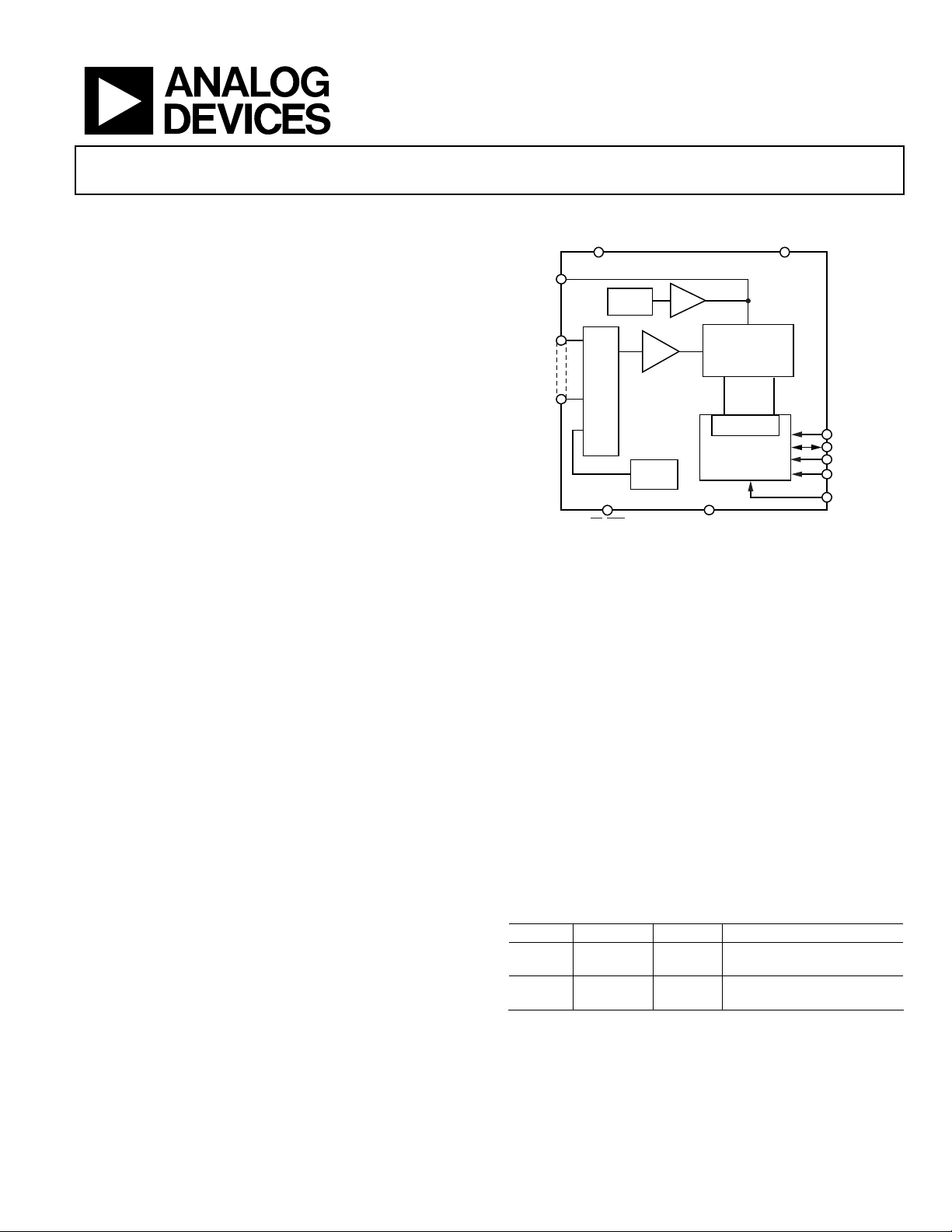
FUNCTIONAL BLOCK DIAGRAM
DD
REF
BUFREF
V
IN0
V
INPUT
IN7
MUX
PD/RST
T/H
AD7291
TEMP
SENSOR
SUCCESSIVE
APPROXIMATION
SEQUENCER
CONTRO L LOG IC
2
I
C INTERFACE
ALERT
Figure 1.
On-chip limit registers can be programmed with high and low
limits for the conversion results; an out-of-range indicator
output (ALERT) becomes active when the programmed high
or low limits are violated by the conversion result. This output
can be used as an interrupt.
PRODUCT HIGHLIGHTS
1. Ideally suited to monitoring system variables in a variety
of systems including telecommunications, process control,
and industrial control.
2
2. I
C-compatible serial interface, which supports standard
and fast modes.
3. Automatic partial power-down while not converting to
maximize power efficiency.
4. Channel sequencer operation.
5. Integrated temperature sensor with 0.25°C resolution.
6. Out of range indicator that can be software disabled or
enabled.
Table 1. AD7291 and Related Products
Device Resolution Interface Features
AD7291
12-bit I
AD7298 12-bit SPI 8-channel, 1 MSPS, 12-bit SAR
2
C 8-channel, I2C, 12-bit SAR
GND
12-BIT
ADC
SCL
SDA
AS1
AS0
V
DRIVE
08711-001
ADC with temperature sensor
ADC with temperature sensor
Rev. B
Information furnished by Analog Devices is believed to be accurate and reliable. However, no
responsibility is assumed by Anal og Devices for its use, nor for any infringements of patents or ot her
rights of third parties that may result from its use. Specifications subject to change without notice. No
license is granted by implication or otherwise under any patent or patent rights of Analog Devices.
Trademarks and registered trademarks are the property of their respective owners.
One Technology Way, P.O. Box 9106, Norwood, MA 02062-9106, U.S.A.
Tel: 781.329.4700 www.analog.com
Fax: 781.461.3113 ©2011 Analog Devices, Inc. All rights reserved.

AD7291 Data Sheet
TABLE OF CONTENTS
Features.............................................................................................. 1
Functional Block Diagram .............................................................. 1
General Description ......................................................................... 1
Product Highlights ........................................................................... 1
Revision History ............................................................................... 2
Specifications..................................................................................... 3
I2C Timing Specifications............................................................ 5
Absolute Maximum Ratings............................................................ 6
Thermal Resistance ...................................................................... 6
ESD Caution.................................................................................. 6
Pin Configuration and Function Descriptions............................. 7
Typical Performance Characteristics ............................................. 8
Terminology .................................................................................... 11
Circuit Information........................................................................ 12
Converter Operation.................................................................. 12
Analog Input............................................................................... 12
ADC Transfer Function............................................................. 13
Temperature Sensor Operation ................................................13
Temperature Sensor Averaging................................................. 13
V
............................................................................................ 14
DRIVE
The Internal or External Reference.......................................... 14
Reset .............................................................................................14
Internal Register Structure............................................................ 15
Address Pointer Register ........................................................... 15
Command Register (0x00)........................................................ 17
Voltage Conversion Result Register (0x01) ............................ 18
T
Conversion Result Register (0x02)................................ 18
SENSE
T
Average Result Register (0x03)...................................... 19
SENSE
Limit Registers (0x04 to 0x1E) ................................................. 19
Hysteresis Register ..................................................................... 20
Alert Status Register A and Alert Status Register B (0x1F and
0x20)............................................................................................. 20
I2C Interface .................................................................................... 21
Serial Bus Address Byte ............................................................. 21
General I2C Timing.................................................................... 21
Writing to the AD7291 .................................................................. 22
Writing Two Bytes of Data to a 16-Bit Register ..................... 22
Writing to Multiple Registers.................................................... 22
Reading Data From the AD7291.................................................. 23
Reading Two Bytes of Data from a 16-Bit Register ............... 23
Modes of Operation ....................................................................... 24
Command Mode ........................................................................ 24
Autocycle Mode.......................................................................... 26
Outline Dimensions....................................................................... 27
Ordering Guide .......................................................................... 27
REVISION HISTORY
10/11—Rev. A to Rev. B
Changes to Table 9.......................................................................... 16
8/11—Rev. 0 to Rev. A
Changes to Temperature Sensor—Internal, Accuracy Parameter,
Table 2 ................................................................................................ 3
1/11—Revision 0: Initial Version
Rev. B | Page 2 of 28

Data Sheet AD7291
SPECIFICATIONS
VDD = 2.8 V to 3.6 V; V
unless otherwise noted.
Table 2.
Parameter Min Typ Max Unit1 Test Conditions/Comments
DYNAMIC PERFORMANCE fIN = 1 kHz sine wave
Signal-to-Noise Ratio (SNR)
Signal-to-Noise (+ Distortion) Ratio (SINAD)
Total Harmonic Distortion (THD)
Spurious-Free Dynamic Range (SFDR)
Intermodulation Distortion (IMD)
Second-Order Terms −88 dB
Third-Order Terms
Channel-to-Channel Isolation −100 dB fIN = 10 kHz
Full Power Bandwidth3 30 MHz At 3 dB
10 MHz At 0.1 dB
DC ACCURACY
Resolution 12 Bits
Integral Nonlinearity (INL)
Differential Nonlinearity (DNL)
Offset Error2 ±2 ±4.5 LSB
Offset Error Matching2 ±2.5 ±4.5 LSB
Offset Temperature Drift 4 ppm/°C
Gain Error2 ±1 ±4 LSB
Gain Error Matching2 ±1 ±2.5 LSB
Gain Temperature Drift 0.5 ppm/°C
ANALOG INPUT
Input Voltage Ranges 0 V
DC Leakage Current ±0.01 ±1 µA
Input Capacitance3 34 pF When in track
8 pF When in hold
REFERENCE INPUT/OUTPUT
Reference Output Voltage
Long-Term Stability 150 ppm For 1000 hours
Output Voltage Hysteresis 50 ppm
Reference Input Voltage Range5 1 2.5 V
DC Leakage Current ±0.01 ±1 µA External reference applied to Pin V
V
Output Impedance
REF
Reference Temperature Coefficient 12 35 ppm/°C
V
Noise3 60 µV rms Bandwidth = 10 MHz
REF
LOGIC INPUTS (SDA, SCL)
Input High Voltage, V
Input Low Voltage, V
Input Current, IIN ±0.01 ±1 µA VIN = 0 V or V
Input Capacitance, C
Input Hysteresis, V
= 1.65 V to 3.6 V; f
DRIVE
2
2
2
2
4
0.7 × V
INH
0.3 × V
INL
3
IN
0.1 × V
HYST
= 400 kHz, fast SCLK mode; V
SCL
70 71 dB
2
70 71 dB
−84 −78 dB
−85 −80 dB
f
−88 dB
±0.5 ±1 LSB
±0.5 ±0.99 LSB Guaranteed no missed codes to 12 bits
2.4925 2.5 2.5075 V ±0.3% maximum at 25°C
1 Ω
V
DRIVE
6 pF
V
DRIVE
= 2.5 V internal/external; TA = −40°C to +125°C,
REF
= 5.4 kHz, fB = 4.6 kHz
A
V
REF
V
DRIVE
DRIVE
REF
Rev. B | Page 3 of 28

AD7291 Data Sheet
Parameter Min Typ Max Unit1 Test Conditions/Comments
LOGIC OUTPUTS
Output High Voltage, VOH V
V
Output Low Voltage, VOL 0.4 V I
0.6 V I
Floating State Leakage Current ±0.01 ±1 µA
Floating State Output Capacitance
3
TEMPERATURE SENSOR—INTERNAL
Operating Range −40 +125 °C
Accuracy ±1 ±2 °C TA = −40°C to +85°C
±1 ±3 °C TA = 85°C to 125°C
Resolution 0.25 °C LSB size
CONVERSION RATE
Conversion Time 3.2 s
Autocycle Update Rate
6
Throughput Rate 22.22 kSPS f
POWER REQUIREMENTS Digital inputs = 0 V or V
V
DD
V
1.65 3 3.6 V
DRIVE
7, 8
I
TOTAL
Normal Mode (Operational) 2.9 3.5 mA
Normal Mode (Static) 2.9 3.3 mA
Full Power-Down Mode 0.3 1.6 A TA = −40°C to +25°C
1.6 4.5 A TA = >25°C to 85°C
4.9 12 A TA = >85°C to 125°C
Power Dissipation
8
Normal Mode (Operational) 8.7 10.5 mW VDD = 3 V, V
10.4 12.6 mW
Normal Mode (Static) 10.4 11.9 mW
Full Power-Down Mode 1.1 5.8 µW TA = −40°C to +25°C
5.8 16.2 µW TA = >25°C to 85°C
17.6 43.2 µW TA = >85°C to 125°C
1
All specifications expressed in decibels are referred to full-scale input, FSR, and tested with an input signal at 0.5 dB below full scale, unless otherwise specified.
2
See the Terminology section.
3
Sample tested during initial release to ensure compliance.
4
Refers to Pin V
5
A correction factor may be required on the temperature sensor results when using an external V
6
Sampled during initial release to ensure compliance; not subject to production testing.
7
I
is the total current flowing in VDD and V
TOTAL
8
I
and power dissipation are specified with VDD = V
TOTAL
specified for 25
REF
o
C.
.
DRIVE
= 3.6 V, unless otherwise noted.
DRIVE
− 0.3 V V
DRIVE
− 0.2 V V
DRIVE
DRIVE
DRIVE
= 3 mA
SINK
= 6 mA
SINK
< 1.8
≥ 1.8
8 pF
50 s
= 400 kHz
SCL
2.8 3 3.6 V
DRIVE
(see the Temperature Sensor Averaging section).
REF
= 3 V
DRIVE
Rev. B | Page 4 of 28
Data Sheet AD7291
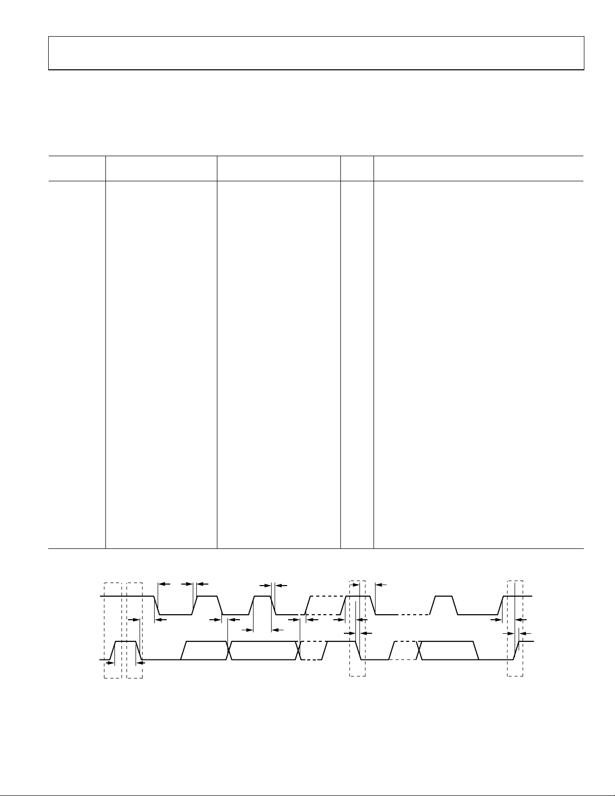
I2C TIMING SPECIFICATIONS
Guaranteed by initial characterization. All values were measured with the input filtering enabled. CB refers to the capacitive load on the
bus line, with t
2.5 V internal/external; T
and tF measured between 0.3 × V
R
= −40°C to +125°C, unless otherwise noted.
A
Table 3.
Limit at T
Parameter Conditions Min Typ Max Unit Description
f
SCL
Standard mode 100 kHz Serial clock frequency
Fast mode 400 kHz
t
1
Standard mode 4 µs t
Fast mode 0.6 µs
t
2
Standard mode 4.7 µs t
Fast mode 1.3 µs
t
3
Standard mode 250 ns t
Fast mode 100 ns
1
t
4
Standard mode 0 3.45 µs t
Fast mode 0 0.9 µs
t
5
Standard mode 4.7 µs t
Fast mode 0.6 µs
t
6
Standard mode 4 µs t
Fast mode 0.6 µs
t
7
Standard mode 4.7 µs t
Fast mode 1.3 µs
t
8
Standard mode 4 µs t
Fast mode 0.6 µs
t9 Standard mode 1000 ns t
Fast mode 20 + 0.1 CB 300 ns
t10 Standard mode 300 ns t
Fast mode 20 + 0.1 CB 300 ns
t11 Standard mode 1000 ns t
Fast mode 20 + 0.1 CB 300 ns
t
Standard mode 1000 ns t
11A
Fast mode 20 + 0.1 CB 300 ns start condition and after an acknowledge bit
t12 Standard mode 300 ns t
Fast mode 20 + 0.1 CB 300 ns
t
SP
t
POWER-UP
1
A device must provide a data hold time for SDA to bridge the undefined region of the SCL falling edge.
Fast mode 0 50 ns Pulse width of the suppressed spike
6 ms Power-up and acquisition time
t
11
t
2
and 0.7 × V
DRIVE
(see Figure 2). VDD = 2.8 V to 3.6 V; V
DRIVE
, T
MIN
MAX
, SCL high time
HIGH
, SCL low time
LOW
, data setup time
SU;DAT
, data hold time
HD;DAT
, setup time for a repeated start condition
SU;STA
, hold time for a repeated start condition
HD;STA
, bus-free time between a stop and a start condition
BUF
, setup time for a stop condition
SU;STO
, rise time of the SDA signal
RDA
, fall time of the SDA signal
FDA
, rise time of the SCL signal
RCL
, rise time of the SCL signal after a repeated
RCL1
, fall time of the SCL signal
FCL
t
12
t
6
= 1.65 V to 3.6 V; V
DRIVE
REF
=
SCL
SDA
t
P PS
S = START CONDITION
P = STOP CONDITI ON
t
6
7
t
4
t
3
t
1
t
5
t
10
S
t
8
t
9
8711-002
Figure 2. 2-Wire Serial Interface Timing Diagram
Rev. B | Page 5 of 28
AD7291 Data Sheet
ABSOLUTE MAXIMUM RATINGS
Table 4.
Parameter Rating
VDD to GND1, GND
V
to GND1, GND −0.3 V to +5 V
DRIVE
−0.3 V to +5 V
Analog Input Voltage to GND1 −0.3 V to +3 V
Digital Input Voltage to GND1
−0.3 V to V
Digital Output Voltage to GND1 −0.3 V to V
V
to GND1 −0.3 V to +3 V
REF
DRIVE
DRIVE
+ 0.3 V
+ 0.3 V
GND to GND1 −0.3 V to +0.3 V
Input Current to Any Pin Except Supplies1 ±10 mA
Operating Temperature Range −40°C to +125°C
Storage Temperature Range −65°C to +150°C
Junction Temperature 150°C
Pb-free Temperature, Soldering
Reflow 260(+0)°C
ESD 2 kV
1
Transient currents of up to 100 mA do not cause latch-up.
Stresses above those listed under Absolute Maximum Ratings
may cause permanent damage to the device. This is a stress
rating only; functional operation of the device at these or any
other conditions above those indicated in the operational
section of this specification is not implied. Exposure to absolute
maximum rating conditions for extended periods may affect
device reliability.
THERMAL RESISTANCE
Table 5. Thermal Resistance
Package Type θJA θ
Unit
JC
20-Lead LFCSP 52 6.5 °C/W
ESD CAUTION
Rev. B | Page 6 of 28
Data Sheet AD7291
T
PIN CONFIGURATION AND FUNCTION DESCRIPTIONS
IN1
IN2
IN0
V
V
19
20
1
V
IN3
2
V
IN4
3
V
IN5
4
V
IN6
5
V
IN7
NOTES
1. THE EXPOSED METAL PADDLE ON THE BOTTOM
OF THE LFCSP PACKAGE SHOULD BE SOLDERED
TO PCB GROUND FOR PROPER HEAT DISSIPATION
AND PERFORMANCE.
AD7291
TOP VIEW
(Not to Scale)
6
7
REF
V
GND1
Figure 3. Pin Configuration
Table 6. Pin Function Descriptions
Pin No. Mnemonic Description
1 to 5,
18 to 20
6 GND1
V
, V
,
IN3
IN4
, V
V
IN5
IN6
V
, V
IN7
IN0
V
, V
IN1
IN2
Analog Inputs. The AD7291 has eight single-ended analog inputs that are multiplexed into the on-chip track-and-
,
hold amplifier. Each input channel can accept analog inputs from 0 V to 2.5 V. Any unused input channels should
,
be connected to GND1 to avoid noise pickup.
Ground. Ground reference point for the internal reference circuitry on the AD7291. All analog input signals and
the external reference signals should be referred to this GND1 voltage. The GND1 pin should be connected to the
ground plane of a system. All ground pins should ideally be at the same potential and must not be more than 0.3 V
apart, even on a transient basis. The V
REF
capacitor.
7 V
REF
Internal Reference/External Reference Supply. The nominal internal reference voltage of 2.5 V appears at this pin.
Provided the output is buffered, the on-chip reference can be taken from this pin and applied externally to the rest
of a system. Decoupling capacitors should be connected to this pin to decouple the reference buffer. For best
performance, it is recommended to use a 10 F decoupling capacitor on this pin to GND1. The internal reference
can be disabled and an external reference supplied to this pin if required. The input voltage range for the external
reference is 2.0 V to 2.5 V.
8 D
CAP
Decoupling Capacitor Pin. Decoupling capacitors (1 F recommended) are connected to this pin to decouple the
internal LDO.
9 GND
Ground. Ground reference point for all analog and digital circuitry on the AD7291. The GND pin should be connected to the ground plane of the system. All ground pins should ideally be at the same potential and must not be
more than 0.3 V apart, even on a transient basis. Both D
10 VDD Supply Voltage, 2.8 V to 3.6 V. This supply should be decoupled to GND with 10 F and 100 nF decoupling capacitors.
11, 13 AS0, AS1
Logic Input. Together, the logic state of these two inputs selects a unique I
for details. The device address depends on the voltage applied to these pins.
12 ALERT
14 SDA
Digital Output. This pin acts as an out-of-range indicator and, if enabled, becomes active when the conversion
result violates the DATA
or DATA
HIGH
register values. See the Limit Registers (0x04 to 0x1E) section.
LOW
Digital Input/Output. Serial bus bidirectional data. This open-drain output requires a pull-up resistor. The output coding
is straight binary for the voltage channels and twos complement for the temperature sensor result.
15 SCL
Digital Input. Serial I
2
C Bus Clock. This input requires a pull-up resistor. The data transfer rate in I2C mode is
compatible with both 100 kHz and 400 kHz operating modes.
16 V
DRIVE
Logic Power Supply Input. The voltage supplied at this pin determines the voltage at which the interface operates.
This pin should be decoupled to GND. The voltage range on this pin is 1.65 V to 3.6 V and may be less than the
but should never exceed it by more than 0.3 V.
DD
17
voltage at V
/RST Power-Down Pin. This pin places the part into a full power-down mode and enables power conservation when
PD
operation is not required. This pin can be used to reset the device by toggling the pin low for a minimum of 1 ns and a
maximum of 100 ns. If the maximum time is exceeded, the part enters power-down mode. When placing the device in
full power-down mode, the analog inputs must be returned to 0 V.
EPAD EPAD
Exposed Paddle. The exposed metal paddle on the bottom of the LFCSP package should be soldered to PCB
ground for proper functionality and heat dissipation.
DRIVE
V
PD/RS
V
16
18
17
15
SCL
14
SDA
13
AS1
ALERT
12
11
AS0
9
8
10
DD
CAP
V
GND
D
08711-003
pin should be decoupled to this ground pin via a 10 F decoupling
and VDD pins should be decoupled to this GND pin.
CAP
2
C address for the AD7291. See Tab le 31
Rev. B | Page 7 of 28
AD7291 Data Sheet
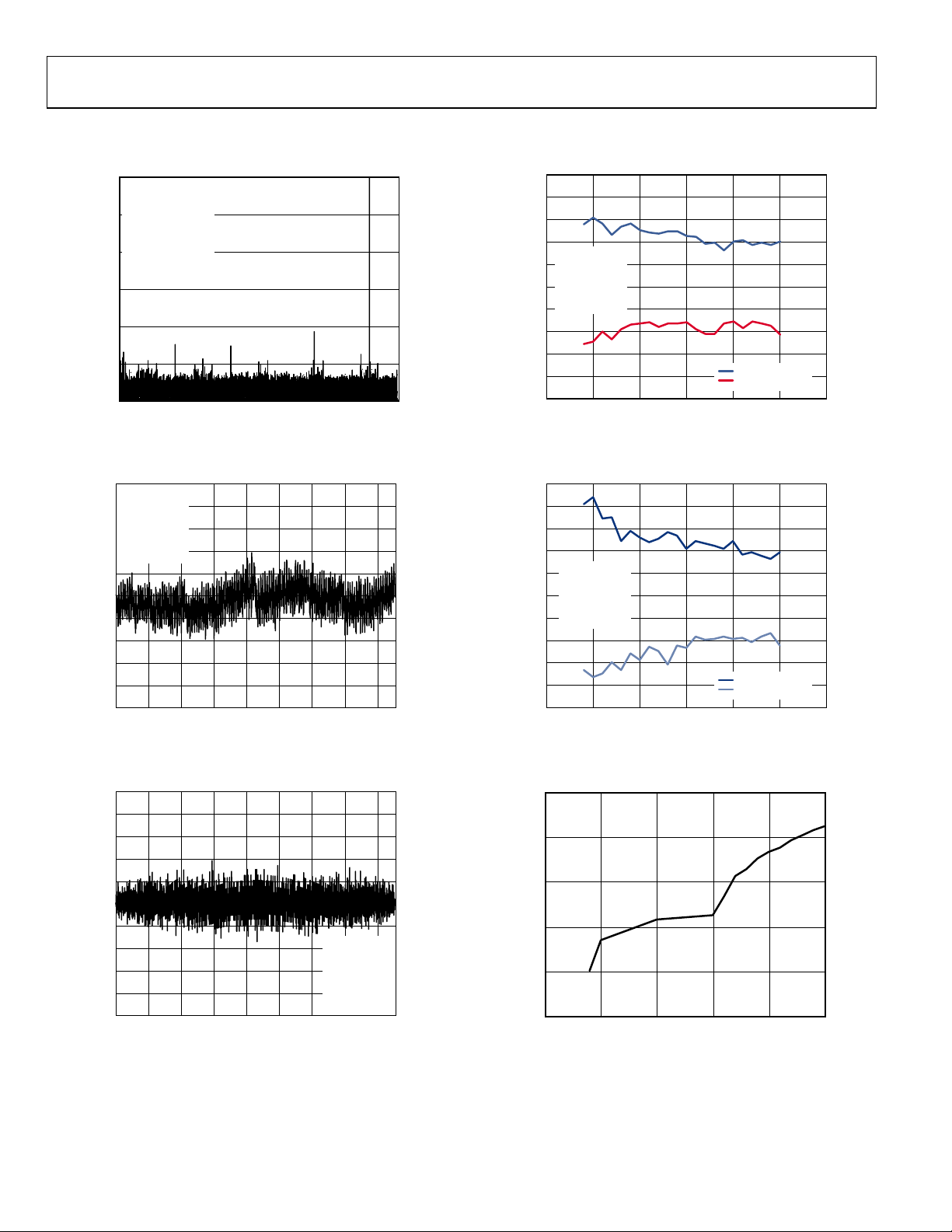
TYPICAL PERFORMANCE CHARACTERISTICS
0
VDD = V
f
= 22.22ksps
S
f
–20
SCL
f
IN
SNR = 71.209
THD = –81.66
–40
–60
AMPLI TUDE (dB)
–80
–100
–120
02k
DRIVE
= 400kHz
= 10kHz
= 3V
4k 6k 8k 10k
FREQUENCY (Hz)
Figure 4. Typical FFT
1.0
TA = 25°C
V
0.8
0.6
0.4
0.2
INL (LSB)
–0.2
–0.4
–0.6
–0.8
–1.0
= 3V
DRIVE
V
= 2.5V
REF
V
= 3V
DD
f
= 22.22ksps
S
f
= 400kHz
SCL
0
0 500 1000 1500 2000 2500 3000 3500 4096
ADC CODE
Figure 5. Typical ADC INL
1.0
0.8
0.6
0.4
0.2
0
DNL (LSB)
–0.2
–0.4
–0.6
–0.8
–1.0
0 500 1000 1500 2000 2500 3000 3500 4096
ADC CODE
TA = 25°C
V
V
V
f
f
Figure 6. Typical ADC DNL
= 3V
DRIVE
= 2.5V
REF
= 3V
DD
= 22.22ksps
S
= 400kHz
SCL
1.0
0.8
0.6
0.4
TA = 25°C
0.2
V
= 3V
DRIVE
V
= 3V
DD
0
f
= 22.22ksps
S
f
INL (LSB)
–0.2
–0.4
–0.6
–0.8
–1.0
08711-009
= 400kHz
SCL
INL (POSITIVE)
INL (NEGATIVE)
0 0.5 1.0 1.5 2.0 2.5 3.0
Figure 7. INL vs. External V
V
(V)
REF
REF
08711-012
1.0
0.8
0.6
0.4
TA = 25°C
0.2
V
= 3V
DRIVE
V
= 3V
0
DD
f
= 22.22ksps
DNL (LSB)
08711-010
S
–0.2
f
= 400kHz
SCL
–0.4
–0.6
–0.8
–1.0
0 0.5 1.0 1.5 2.0 2.5 3.0
V
(V)
REF
Figure 8. DNL vs. External V
DNL (POSITIVE)
DNL (NEGATIVE)
REF
08711-013
11.7
11.6
11.5
11.4
EFFECTIVE NUMBER OF BITS
11.3
11.2
08711-011
0 0.5 1.0 1.5 2.0 2.5
Figure 9. Effective Number of Bits vs. V
EXTERNAL REF ERENCE (V)
REF
, f
= 400 kHz
SCL
08711-035
Rev. B | Page 8 of 28
Data Sheet AD7291
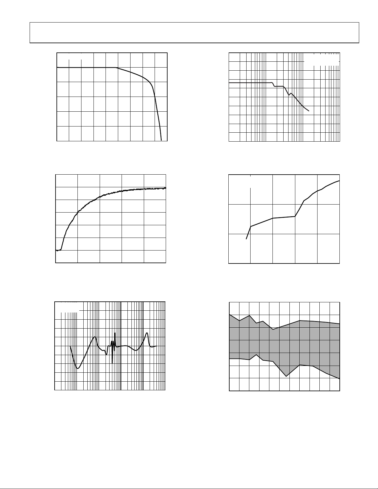
R
A
–
3.0
VDD = V
2.5
2.0
(V)
1.5
REF
V
1.0
0.5
0
0 0.5 1.0 1.5 2.0 2.5 3.0 3.5 4.0 4.5
= 3V
DRIVE
Figure 10. V
CURRENT LOAD (mA)
vs. Reference Output Drive
REF
55
50
08711-021
125
120
115
110
105
100
95
90
85
80
CHANNEL-TO-CHANNEL ISOLATION (d B)
75
1 10 100 1k
f
NOISE
(kHz)
Figure 13. Channel-to-Channel Isolation, f
VDD = V
f
= 400kHz
SCL
= 10 kHz
IN
72
V
= 3V
DRIVE
V
= 3V
DD
DRIVE
= 3V
08711-018
45
40
35
TURE READING (°C)
30
TEMPE
25
20
0 20406080100
TIME (Seconds)
08711-014
Figure 11. Response to Thermal Shock from Room Temperature into 50°C
Stirred Oil
90
VDD = 3V
V
= 3V
DRIVE
–92
–94
–96
–98
–100
PSRR (dB)
–102
–104
–106
–108
–110
1k 10k 100k 1M 10M 100M
RIPPLE FREQUENCY (Hz)
Figure 12. PSRR vs. Supply Ripple Frequency Without Supply Decoupling
71
SINAD (dB)
70
69
022.01.51.00.5
Figure 14. SINAD vs. Reference Voltage, f
EXTERNAL REF E RENCE (V)
= 400 kHz, fs = 22.22 kSPS
SCL
.5
08711-036
1.5
1.0
0.5
0
–0.5
–1.0
TEMPERATURE ERROR (°C)
–1.5
–2.0
–40 –25 –10 5 20 35 50 65 80 95 110 125
08711-061
TEMPERATURE (°C)
08711-017
Figure 15. Temperature Accuracy at 3 V
Rev. B | Page 9 of 28

AD7291 Data Sheet
9.0
V
= 3V
DRIVE
8.9
8.8
8.7
8.6
8.5
8.4
POWER (mW)
8.3
8.2
8.1
8.0
= 3V
V
DD
0 60 120 180 240 300 360 420
SCL FREQUENCY (kHz)
08711-062
Figure 16. Power vs. Throughput in Normal Mode
2.5
V
= 3V
DRIVE
2.0
1.5
1.0
TOTAL CURRE NT (µA)
0.5
0
2.7 2.9 3.1 3.3 3.52.8 3.0 3.2 3.4 3.6
V
DD
Figure 17. Full Shutdown Current vs. Supply Voltage for Various
Temperatures
–40°C
+25°C
+85°C
+125°C
08711-037
Rev. B | Page 10 of 28

Data Sheet AD7291
TERMINOLOGY
Signal-to-Noise and Distortion Ratio (SINAD)
The measured ratio of signal-to-noise and distortion at the
output of the ADC. The signal is the rms amplitude of the
fundamental. Noise is the sum of all nonfundamental signals
up to half the sampling frequency (f
/2), excluding dc. The
S
ratio is dependent on the number of quantization levels in the
digitization process; the more levels, the smaller the quantization
noise. The theoretical signal-to-noise and distortion ratio for
an ideal N-bit converter with a sine wave input is given by
Signal-to-(Noise + Distortion) = (6.02 N + 1.76) dB
Thus, the SINAD is 74 dB for an ideal 12-bit converter.
Total Harmonic Distortion (THD)
The ratio of the rms sum of harmonics to the fundamental. For
the AD7291, it is defined as
2
2
2
2
THD
2
2
log20)dB(
=
4
3
V
1
VVVVV
++++
6
5
where:
V
is the rms amplitude of the fundamental.
1
, V3, V4, V5, and V6 are the rms amplitudes of the second
V
2
through sixth harmonics.
Peak Harmonic or Spurious Noise
The ratio of the rms value of the next largest component in the
ADC output spectrum (up to f
/2 and excluding dc) to the rms
S
value of the fundamental. Typically, the value of this specification
is determined by the largest harmonic in the spectrum, but for
ADCs where the harmonics are buried in the noise floor, it is a
noise peak.
Intermodulation Distortion
With inputs consisting of sine waves at two frequencies, fa and
fb, any active device with nonlinearities creates distortion
products at sum and difference frequencies of mfa ± nfb, where
m, n = 0, 1, 2, 3, and so on. Intermodulation distortion terms
are those for which neither m nor n equals zero. For example,
second-order terms include (fa + fb) and (fa − fb), while thirdorder terms include (2fa + fb), (2fa − fb), (fa + 2fb), and (fa − 2fb).
The AD7291 is tested using the CCIF standard where two input
frequencies near the top end of the input bandwidth are used.
In this case, the second-order terms are usually distanced in
frequency from the original sine waves while the third-order
terms are usually at a frequency close to the input frequencies.
As a result, the second- and third-order terms are specified
separately. The calculation of intermodulation distortion is,
like the THD specification, the ratio of the rms sum of the
individual distortion products to the rms amplitude of the sum
of the fundamentals, expressed in dB.
Aperture Delay
The measured interval between the sampling clock’s leading
edge and the point at which the ADC takes the sample.
Aperture Jitter
This is the sample-to-sample variation in the effective point in
time at which the sample is taken.
Full-Power Bandwidth
The input frequency at which the amplitude of the reconstructed fundamental is reduced by 0.1 dB or 3 dB for a
full-scale input.
Power Supply Rejection Ratio (PSRR)
PSRR is defined as the ratio of the power in the ADC output at
full-scale frequency, f, to the power of a 100 mV p-p sine wave
applied to the ADC V
supply of frequency, fS. The frequency
DD
of the input varies from 5 kHz to 25 MHz.
PSRR (dB) = 10 log(Pf/Pf
)
S
where:
Pf is the power at frequency, f, in the ADC output.
Pf
is the power at frequency, fS, in the ADC output.
S
Integral Nonlinearity
The maximum deviation from a straight line passing through
the endpoints of the ADC transfer function. The endpoints are
zero scale, a point 1 LSB below the first code transition, and full
scale, a point 1 LSB above the last code transition.
Differential Nonlinearity
The difference between the measured and the ideal 1 LSB
change between any two adjacent codes in the ADC.
Offset Error
The deviation of the first code transition (00…000) to
(00…001) from the ideal—that is, GND1 + 1 LSB.
Offset Error Match
The difference in offset error between any two channels.
Gain Error
The deviation of the last code transition (111…110) to
(111…111) from the ideal (that is, V
− 1 LSB) after the offset
REF
error has been adjusted out.
Gain Error Match
The difference in gain error between any two channels.
Track-and-Hold Acquisition Time
The track-and-hold amplifier returns to track mode at the end
of conversion. Track-and-hold acquisition time is the time
required for the output of the track-and-hold amplifier to reach
its final value, within ±1 LSB, after the end of conversion.
Rev. B | Page 11 of 28

AD7291 Data Sheet
CIRCUIT INFORMATION
The AD7291 includes an 8-channel multiplexer, an on-chip
track-and-hold amplifier, an analog-to-digital converter (ADC),
an on-chip oscillator, internal data registers, an internal temperature sensor, and an I
2
C-compatible serial interface, all housed in
a 20-lead LFCSP. This package offers considerable space-saving
advantages over alternative solutions. The part can be operated
from a single supply from 2.8 V to 3.6 V and offers 12 bits of
resolution. The AD7291 has eight single-ended input channels
and an on-chip ±12 ppm reference. The analog input range for
the AD7921 is 0 V to V
. The AD7291 includes a high
REF
accuracy band gap temperature sensor, which is monitored and
digitized by the 12-bit ADC to give a resolution of 0.25°C.
The AD7291 typically remains in a partial power-down state
while not converting. When supplies are first applied, the part
powers up in a partial power-down state. Power-up is initiated
prior to a conversion, and the device returns to partial powerdown mode when the conversion is complete. Conversions can
be initiated by using the autocycle mode or command mode
where wake-up and a conversion occur during a write address
function. When the conversion is complete, the AD7291 again
enters partial power-down mode.
In command mode at the beginning of a read, the AD7291
wakes up completely, that is, becomes fully functional and
completes the conversion while the address is being read out. In
autocylce mode, conversions occur at 50 µs intervals; that is, the
AD7291 exits partial power-down mode and powers up fully at
50 µs intervals. This automatic partial power-down feature
allows power saving between conversions. Any read or write
operation across the I
2
C interface can occur while the device is
in partial power-down mode.
CONVERTER OPERATION
The AD7291 is a 12-bit successive approximation ADC based
around a capacitive DAC. Figure 18 and Figure 19 show simplified schematics of the ADC during the acquisition and conversion
phase, respectively. The ADC comprises control logic, SAR,
and a capacitive DAC that are used to add and subtract fixed
amounts of charge from the sampling capacitor to bring the
comparator back into a balanced condition. Figure 18 shows the
acquisition phase. SW2 is closed and SW1 is in Position A, the
comparator is held in a balanced condition, and the sampling
capacitor acquires the signal on the selected V
A
V
IN
SW1
B
SW2
GND1
Figure 18. ADC Acquisition Phase
COMPARATOR
channel.
IN
CAPACITIVE
DAC
CONTROL
LOGIC
08711-004
When the ADC starts a conversion (see Figure 19), SW2
opens and SW1 moves to Position B, causing the comparator
to become unbalanced. The control logic and the capacitive
DAC are used to add and subtract fixed amounts of charge to
bring the comparator back into a balanced condition. When the
comparator is rebalanced, the conversion is complete. The
control logic generates the ADC output code. Figure 21 shows
the transfer functions of the ADC.
CAPACITIVE
DACE
A
V
GND1
IN
SW1
B
SW2
COMPARATOR
Figure 19. ADC Conversion Phase
CONTROL
LOGIC
08711-005
ANALOG INPUT
Figure 20 shows an equivalent circuit of the analog input structure of the AD7291. The two diodes, D1 and D2, provide ESD
protection for the analog inputs. Care must be taken to ensure
that the analog input signal never exceeds the internally generated
LDO voltage of 2.5 V (D
the diodes to become forward biased and start conducting
current into the substrate. The maximum current these diodes
can conduct without causing irreversible damage to the part is
10 mA. Capacitor C1, in Figure 20, is typically about 8 pF and
can primarily be attributed to pin capacitance. Resistor R1 is a
lumped component made up of the on resistance of a switch
(track-and-hold switch) and the on resistance of the input
multiplexer. The total resistance is typically about 155 .
Capacitor C2 is the ADC sampling capacitor and has a
capacitance of 34 pF typically.
D
CAP
D1
V
IN
D2
C1
8pF
Figure 20. Equivalent Analog Input Circuit
For ac applications, removing high frequency components
from the analog input signal is recommended by using an RC
low-pass filter on the relevant analog input pin. In applications
where harmonic distortion and signal-to-noise ratios are
critical, the analog input should be driven from a low impedance source. Large source impedances significantly affect the
ac performance of the ADC. This may necessitate the use of
an input buffer amplifier. The choice of the op amp is a function
of the particular application performance criteria.
) by more than 300 mV. This causes
CAP
(2.5V)
C2
34pF
R1
CONVERSION PHASE: SWITCH OPEN
TRACK PHASE: SWITCH CLOSED
08711-006
Rev. B | Page 12 of 28

Data Sheet AD7291
V
ADC TRANSFER FUNCTION
The output coding of the AD7291 is straight binary for the
analog input channel conversion results and twos complement
for the temperature conversion result. The designed code transitions occur at successive LSB values (that is, 1 LSB, 2 LSBs,
and so forth). The LSB size is V
/4096 for the AD7291. The
REF
ideal transfer characteristic for the AD7291 for straight binary
coding is shown in Figure 21.
111...111
111...110
111...000
011...111
ADC CODE
NOTES
1. V
REF
000...010
000...001
000...000
0V
IS 2.5V.
Figure 21. Straight Binary Transfer Characteristic
1LSB = V
REF
ANALOG INPUT
+V
REF
/4096
– 1LSB1LSB
08711-007
TEMPERATURE SENSOR OPERATION
The AD7291 contains one local temperature sensor. The on-chip,
band gap temperature sensor measures the temperature of the
AD7291 die.
The temperature sensor module on the AD7291 is based on the
three current principle (see Figure 22), where three currents are
passed through a diode and the forward voltage drop is
measured, allowing the temperature to be calculated free of
errors caused by series resistance.
BIAS
DIODE
DD
V
OUT+
TO ADC
V
OUT–
I4 × I
INTERNAL
SENSE
TRANSISTOR
8 × I I
BIAS
Each input integrates, in turn, over a period of several hundred
microseconds. This takes place continuously in the background,
leaving the user free to perform conversions on the other
channels. When integration is complete, a signal passes to the
control logic to initiate a conversion automatically.
If the ADC is in command mode and performing a voltage
conversion, the AD7291 waits for it to complete and then
initiates a temperature sensor conversion. If the ADC is not
performing voltage conversions, temperature conversions occur
at 5 ms inter vals.
In autocycle mode, the conversion is inserted into an
appropriate place in the current sequence. If the ADC is idle,
the conversion takes place immediately. The T
conversion
SENSE
result register stores the result of the last conversion on the
temperature channel; this can be read at any time.
Theoretically, the temperature measuring circuit can measure
temperatures from −512°C to +511°C with a resolution of
0.25°C. However, temperatures outside T
(the specified tem-
A
perature range for the AD7291) are outside the guaranteed
operating temperature range of the device. The temperature
sensor is enabled by setting the TSENSE bit in the command
register.
TEMPERATURE SENSOR AVERAGING
The AD7291 incorporates a temperature sensor averaging
feature to enhance the accuracy of the temperature measurements. The temperature averaging feature is performed
continuously in the background provided the TSENSE bit
in the command register is enabled. The temperature is
measured each time a T
moving average method is used to determine the result in the
T
average result register. The average result is given by the
SENSE
following equation:
7
SENSE
()
8
The average result is then available in the T
register whose content is updated after every T
The first T
conversion result given by the AD7291 after the
SENSE
temperature sensor has been selected in the command register
(Bit D7) is the actual first T
result remains valid until the next T
completed and the result register is updated.
conversion is performed and a
SENSE
1
__
conversion result, and this
SENSE
()
+=
8
average result
SENSE
SENSE
conversion is
SENSE
ResultCurrentResultAveragePreviousAVGT
_
conversion.
08711-008
Figure 22. Top Level Structure of Internal Temperature Sensor
Rev. B | Page 13 of 28

AD7291 Data Sheet
Temperature Value Format
One LSB of the ADC corresponds to 0.25°C. The temperature
reading from the ADC is stored in a 12-bit twos complement
format, to accommodate both positive and negative temperature measurements. Sample temperature values are listed in
Tabl e 7 . The temperature conversion formulas are as follows:
Positive Temperature = ADC Code/4
Negative Temperature = (4096 − ADC Code)/4
The previous formulae are for a V
of 2.5 V only. If an
REF
external reference is used, the temperature sensor requires an
external reference of between 2 V and 2.5 V for correct
operation. The temperature results (in Celsius) are calculated
using the following formula, where V
is the value of the
EXT_REF
external reference voltage.
ADCCode
⎛
VeTemperatur
⎜
_
REFEXT
10
⎝
⎞
+=
15.2733.109
−
⎟
⎠
Table 7. Temperature Data Format
Temperature (°C) Digital Output
−40 1111 0110 0000
−25 1111 1001 1100
−10 1111 1101 1000
−0.25 1111 1111 1111
0 0000 0000 0000
+0.25 0000 0000 0001
+10 0000 0010 1000
+25 0000 0110 0100
+50 0000 1100 1000
+75 0001 0010 1100
+100 0001 1001 0000
+105 0001 1010 0100
+125 0001 1111 0100
V
DRIVE
V
controls the voltage at which the serial interface operates.
DRIVE
allows the ADC to easily interface to both 1.8 V and 3 V
V
DRIVE
processors. For example, if the AD7291 is operated with a V
of 3.3 V, the V
pin can be powered from a 1.8 V supply.
DRIVE
DD
This enables the AD7291 to operate with a larger dynamic
range with a V
1.8 V processors. Take care to ensure that V
exceed V
of 3.3 V while still being able to interface to
DD
does not
DRIVE
by more than 0.3 V (see the Absolute Maximum
DD
Ratings section).
THE INTERNAL OR EXTERNAL REFERENCE
The AD7291 can operate with either the internal 2.5 V on-chip
reference or an externally applied reference. The EXT_REF bit
in the command register is used to determine whether the
internal reference is used. If the EXT_REF bit is selected in the
command register, an external reference can be supplied
through the V
pin. On power-up, the internal reference is
REF
enabled. Suitable external reference sources for the AD7291
include AD780, AD1582, ADR431, REF193, and ADR391.
The internal reference circuitry consists of a 2.5 V band gap
reference and a reference buffer. When the AD7291 operates in
internal reference mode, the 2.5 V internal reference is available
at the V
pin, which should be decoupled to GND1 using a
REF
10 F capacitor. It is recommended that the internal reference
be buffered before applying it elsewhere in the system.
The internal reference is capable of sourcing up to 2 mA of
current when the converter is static. The reference buffer
requires 5.5 ms to power up and charge the 10 F decoupling
capacitor during the power-up time.
RESET
The AD7291 includes a reset feature, which can be used to reset
the device and the content of all internal registers including the
command register to their default state. To activate the reset
PD
operation, the
minimum of 1 ns and a maximum of 100 ns and be asynchronous
to the clock; therefore, it can be triggered at any time. If the
RST
pin is held low for greater than 100 ns, the part enters full
power-down mode. It is imperative that the
at a stable logic level at all times to ensure normal operation.
RST
/
pin should be brought low for a
PD
RST
/
pin be held
PD
/
Rev. B | Page 14 of 28

Data Sheet AD7291
INTERNAL REGISTER STRUCTURE
The AD7291 contains 34 internal registers (see Figure 23) that
are used to store conversion results, high and low conversion
limits, and information to configure and control the device.
There are 33 data registers and one address pointer register.
Each data register has an address that the address pointer
register points to when communicating with it. Tab l e 9 details
which registers are read, write, or read/write.
ADDRESS POINTER REGISTER
The address pointer register is the register to which the first
data byte of every write operation is written automatically;
therefore, this register does not have and does not require an
address. The address pointer register is an 8-bit register in
which the six LSBs are used as pointer bits to store an address
that points to one of the AD7291’s data registers. The first byte
following each write address is to the address pointer register,
containing the address of one of the data registers. The six LSBs
select the data register to which subsequent data bytes are
written. Only the six LSBs of this register are used to select a
data register. During power-up, the address pointer register
contains all 0s, pointing to the command register.
Table 8. Address Pointer Register
D1 D0 P5 P4 P3 P2 P1 P0
0 0 Register select
ADDRESS
POINTER
REGISTER
COMMAND
REGISTER
VOLTAG E CONV
RESULT REGISTER
T
CONV
SENSE
RESULT REGISTER
T
AVG
SENSE
RESULT REGISTER
CH0 DATA
HIGH
REGISTER
CH0 DATA
CH0 HYSTERESI S
CH1 DATA
CH1 DATA
CH1 HYSTERESIS
CH7 DATA
CH7 DATA
CH7 HYSTERESI S
T
SENSE
T
SENSE
T
SENSE
ALERT STATUS
ALERT STATUS
LOW
REGISTER
REGISTER
HIGH
REGISTER
LOW
REGISTER
REGISTER
HIGH
REGISTER
LOW
REGISTER
REGISTER
DATA
REGISTER
DATA
REGISTER
HYSTERESIS
REGISTER
REGISTER A
REGISTER B
HIGH
LOW
DATA
SDA
SCL
Rev. B | Page 15 of 28
SERIAL BUS I NT ERFACE
Figure 23. AD7291 Register Structure
08711-015

AD7291 Data Sheet
Table 9. AD7291 Register Addresses
Hex Code P5 P4 P3 P2 P1 P0 Registers Read/Write
0x00 0 0 0 0 0 0 Command register Write.
0x01 0 0 0 0 0 1 Voltage conversion result register Read.
0x02 0 0 0 0 1 0 T
0x03 0 0 0 0 1 1 T
0x04 0 0 0 1 0 0 CH0 DATA
0x05 0 0 0 1 0 1 CH0 DATA
0x06 0 0 0 1 1 0 CH0 hysteresis register Read/write.
0x07 0 0 0 1 1 1 CH1 DATA
0x08 0 0 1 0 0 0 CH1DATA
0x09 0 0 1 0 0 1 CH1 hysteresis register Read/write.
0x0A 0 0 1 0 1 0 CH2 DATA
0x0B 0 0 1 0 1 1 CH2 DATA
0x0C 0 0 1 1 0 0 CH2 hysteresis register Read/write.
0x0D 0 0 1 1 0 1 CH3 DATA
0x0E 0 0 1 1 1 0 CH3 DATA
0x0F 0 0 1 1 1 1 CH3 hysteresis register Read/write.
0x10 0 1 0 0 0 0 CH4 DATA
0x11 0 1 0 0 0 1 CH4 DATA
0x12 0 1 0 0 1 0 CH4 hysteresis register Read/write.
0x13 0 1 0 0 1 1 CH5 DATA
0x14 0 1 0 1 0 0 CH5 DATA
0x15 0 1 0 1 0 1 CH5 hysteresis register Read/write.
0x16 0 1 0 1 1 0 CH6 DATA
0x17 0 1 0 1 1 1 CH6 DATA
0x18 0 1 1 0 0 0 CH6 hysteresis register Read/write.
0x19 0 1 1 0 0 1 CH7 DATA
0x1A 0 1 1 0 1 0 CH7 DATA
0x1B 0 1 1 0 1 1 CH7 hysteresis register Read/write.
0x1C 0 1 1 1 0 0 T
0x1D 0 1 1 1 0 1 T
0x1E 0 1 1 1 1 0 T
0x1F 0 1 1 1 1 1 Alert Status Register A Read.
0x20 1 0 0 0 0 0 Alert Status Register B Read.
0x3F 1 1 1 1 1 1 Factory test mode The user should not access this register.
conversion result register Read.
SENSE
average result register Read.
SENSE
register Read/write.
HIGH
register Read/write.
LOW
register Read/write.
HIGH
register Read/write.
LOW
register Read/write.
HIGH
register Read/write.
LOW
register Read/write.
HIGH
register Read/write.
LOW
register Read/write.
HIGH
register Read/write.
LOW
register Read/write.
HIGH
register Read/write.
LOW
register Read/write.
HIGH
register Read/write.
LOW
register Read/write.
HIGH
register Read/write.
LOW
DATA
SENSE
DATA
SENSE
hysteresis register Read/write.
SENSE
register Read/write.
HIGH
register Read/write.
LOW
Rev. B | Page 16 of 28

Data Sheet AD7291
COMMAND REGISTER (0x00)
The command register is a 16-bit write-only register that is used to set the operating modes of the AD7291. The bit functions are outlined
in Tab l e 1 0 . A two-byte write is necessary when writing to the command register. MSB denotes the first bit in the data stream. During
power-up, the default content of the command register is all 0s.
Table 10. Command Register Bits and Default Settings at Power-Up
Channel Bit D15 to DB8 D7 D6 D5 D4 D3 D2 D1 D0
Function
Setting
MSB
CH0 to CH7 TSENSE Don’t
Enable = 1
Disable = 0
Table 11. Command Register Bit Function Descriptions
Bit Mnemonic Comment
D15 to D8 CH0 to CH7
D7 TSENSE
D6 Don’t care
D5
Noisedelayed bit
trial and
sampling
D4 EXT_REF
D3
Polarity of
ALERT pin
D2 Clear alert
D1 RESET
D0
Autocycle
mode
Enable = 1
Disable = 0
care
0 Enable = 1
Noise-delayed
bit trial and
sampling
Disable = 0
EXT_REF Polarity of ALERT
Enable = 1
Disable = 0
pin (active high/
active low)
Active low = 1
Active high = 0
Clear alert RESET Autocycle
Enable = 1
Disable = 0
Enable = 1
Disable = 0
LSB
mode
Enable = 1
Disable = 0
These 8-channel address bits select the analog input channel(s) to be converted. A 1 in any of Bit D15 to
Bit D8 selects a channel for conversion. If more than one channel bit is set to 1, the AD7291 sequences
through the selected channels, starting with the lowest channel. All unused channels should be set to 0. A
channel or sequence of channels for conversion must be selected in the command register, prior to initiating
a conversion.
This bit enables temperature conversions, which occur in the background at 5 ms intervals. The results can be
read from the T
conversion result register (0x02) and the T
SENSE
average result register (0x03). For details,
SENSE
refer to the Temperature Sensor Operation section.
When this function is enabled, it delays the critical sampling intervals and bit trials when there is activity on
2
C bus, thus ensuring improved dc performance of the AD7291. When this feature is enabled, the
the I
conversion time may vary. This bit is disabled on power-up, and it is recommended to write a 1 to enable this
feature for normal operation.
Writing a Logic 1 to this bit enables the use of an external reference. The input voltage range for the external
reference is 2 V to 2.5 V. The external reference should not exceed 2.5 V or the device performance will be
adversely affected. During power-up, the default configuration has the internal reference enabled.
This bit determines the active polarity of the ALERT pin. The ALERT pin is configured for active low operation
if this bit is set to 1 and active high if this bit is set to 0. The default configuration on power-up is active high (0).
This bit clears the content of the alert status register. Once the content of both alert status registers is cleared,
this bit should be reprogrammed to a Logic 0 to ensure that future alerts are detected.
Setting this bit resets the contents of all internal registers in the AD7291 to their default states including the
command register itself. This bit is automatically returned to 0 once the reset is completed to enable the
internal registers to be reprogrammed.
Writing a 1 to this bit enables the autocycle mode of operation. In this mode, the channels selected in Bit D15
to Bit D8 are continuously converted by the AD7291. This function is used in conjunction with the limit
registers, which can be programmed to issue an alert if the conversion result exceeds the preset limit for any
channel selected for conversion.
Rev. B | Page 17 of 28

AD7291 Data Sheet
Table 12. Channel Selection Bits for Command Register
D15 D14 D13 D12 D11 D10 D9 D8 Selected Analog Input Channel Comments
0 0 0 0 0 0 0 0 No channel selected
0 0 0 0 0 0 0 1 Convert on Channel 7 (V
0 0 0 0 0 0 1 0 Convert on Channel 6 (V
0 0 0 0 0 1 0 0 Convert on Channel 5 (V
0 0 0 0 1 0 0 0 Convert on Channel 4 (V
0 0 0 1 0 0 0 0 Convert on Channel 3 (V
0 0 1 0 0 0 0 0 Convert on Channel 2 (V
0 1 0 0 0 0 0 0 Convert on Channel 1 (V
1 0 0 0 0 0 0 0 Convert on Channel 0 (V
)
IN7
)
IN6
)
IN5
)
IN4
)
IN3
)
IN2
)
IN1
)
IN0
If more than one channel is
selected, the AD7291 converts the
selected channels starting with the
lowest channel in the sequence.
Table 13. T
Data Format
SENSE
Input D11 (MSB) D10 D9 D8 D7 D6 D5 D4 D3 D2 D1 D0 (LSB)
Value (°C)
Sample Delay and Bit Trial Delay
Ideally, no I2C bus activity should occur while an ADC
conversion is taking place. However, this may not be possible,
for example, when operating in autocycle mode. It is therefore
recommended to enable the noise delayed bit trial and sampling
function by writing a 1 to Bit D5 in the command register. This
mechanism delays critical sample intervals and bit trials while
there is activity on the I
each bit decision, and conversion results are less susceptible to
interference from external noise.
On power-up, the bit trial and sample interval delay mechanism
is not enabled. It is recommended that this feature should be
enabled for normal operation. When enabled, the AD7291
delays the bit trials, mitigating against the effect of activity on
2
the I
C bus. In cases where there is excessive activity on the
interface lines, enabling these bits may cause the overall
conversion time to increase.
The AD7291 also incorporates functionality that allows it to
reject glitches shorter than 50 ns. This feature improves the
noise susceptibility of the device.
VOLTAGE CONVERSION RESULT REGISTER (0x01)
The voltage conversion result register is a 16-bit read-only
register that stores the conversion result from the ADC in
straight binary format. A 2-byte read is necessary to read data
from this register. Ta bl e 14 and Ta bl e 15 show the contents of
the first and second bytes of data to be read from the AD7291.
Each AD7291 conversion result consists of four channel address
bits (see Ta b le 1 4 and Ta b le 1 5) and the 12-bit data result.
Bit D15 to Bit D12 are the channel address bits that identify
the ADC channel that corresponds to the subsequent result.
Bit D11 to Bit D0 contain the most recent ADC result.
−512 +256 +128 +64 +32 +16 +8 +4 +2 +1 +0.5 +0.25
Table 14. Conversion Value Register (First Read)
MSB
D15 D14 D13 D12 D11 D10 D9 D8
ADD3 ADD2 ADD1 ADD0 B11 B10 B9 B8
Table 15. Conversion Value Register (Second Read)
LSB
2
C bus. This results in a quiet period for
D7 D6 D5 D4 D3 D2 D1 D0
B7 B6 B5 B4 B3 B2 B1 B0
Table 16. Channel Address Bits for the Result Register
ADD2 ADD2 ADD1 ADD0 Analog Input Channel
0 0 0 0 V
0 0 0 1 V
0 0 1 0 V
0 0 1 1 V
0 1 0 0 V
0 1 0 1 V
0 1 1 0 V
0 1 1 1 V
1 0 0 0 T
1 0 0 1 T
IN0
IN1
IN2
IN3
IN4
IN5
IN6
IN7
SENSE
average result
SENSE
Temperature Value Format
The temperature reading from the ADC is stored in an 11-bit
twos complement format, D11 to D0, to accommodate both
positive and negative temperature measurements. The temperature data format is provided in Tabl e 1 3 .
T
CONVERSION RESULT REGISTER (0x02)
SENSE
The T
result register is a 16-bit read-only register used to
SENSE
store the ADC data generated from the internal temperature
sensor. This register stores the temperature readings from the
ADC in a 12-bit twos complement format, D11 to D0, and
uses Bit D15 to Bit D12 to store the channel address bits.
Conversions take place approximately every 5 ms. Tab le 1 3
details the temperature data format that applies to the internal
temperature sensor.
Rev. B | Page 18 of 28

Data Sheet AD7291
Table 17. T
MSB
D15 D14 D13 D12 D11 D10 D9 D8
ADD3 ADD2 ADD1 ADD0 B11 B10 B9 B8
Table 18. T
LSB
D7 D6 D5 D4 D3 D2 D1 D0
B7 B6 B5 B4 B3 B2 B1 B0
T
AVERAGE RESULT REGISTER (0x03)
SENSE
The T
SENSE
used to store the average result from the internal temperature
sensor. This register stores the average temperature readings
from the ADC in an 11-bit twos complement format, D11 to
D0, and uses Bit D15 to Bit D12 to store the channel address
bits. The T
T
conversion is completed. The first T
SENSE
conversion result given by the AD7291 after averaging is
enabled is the actual first T
details the temperature data format, which applies to the
internal temperature sensor. See the Temperature Sensor
Ave raging section for more details.
Table 19. T
MSB
D15 D14 D13 D12 D11 D10 D9 D8
ADD3 ADD2 ADD1 ADD0 B11 B10 B9 B8
Table 20. T
LSB
D7 D6 D5 D4 D3 D2 D1 D0
B7 B6 B5 B4 B3 B2 B1 B0
LIMIT REGISTERS (0x04 TO 0x1E)
The AD7291 has nine pairs of limit registers. Each pair stores
high and low conversion limits for each analog input channel
and the internal temperature sensor. Each pair of limit registers
has one associated hysteresis register. All 27 registers are 16 bits
wide; only the 12 LSBs of the registers are used for the AD7291.
The four MSBs, D15 and D12, in these registers should contain
0s. During power-up, the contents of the DATA
each analog voltage channel is full scale (0x0FFF), while the
default contents of the DATA
zero scale (0x0000). The output coding of the AD7291 is twos
complement for the temperature conversion result. The default
content for the T
default content of the T
AD7291 signals an alert in hardware if the conversion result
moves outside the upper or lower limit set by the limit registers.
Conversion Result Register (First Read)
SENSE
Result Register (Second Read)
SENSE
average result register is a 16-bit read-only register
average result register is updated after every
SENSE
average
SENSE
conversion result. Tabl e 13
SENSE
Average Result Register (First Read)
SENSE
Average Result Register (Second Read)
SENSE
register for
HIGH
voltage channels registers is
LOW
SENSE
DATA
SENSE
register is 0x07FF, while the
HIGH
DATA
register is 0x0800. The
LOW
DATA
The DATA
Register
HIGH
HIGH
registers for CH0 to CH7 and the internal
temperature sensor are 16-bit read/write registers; only the
12 LSBs of each register are used. Bit D15 to Bit D12 are not
used in the register and are set to 0s. This register stores the
upper limit that activates the ALERT output. If the value in the
conversion result register is greater than the value in the
DATA
register, an ALERT occurs for that channel. When
HIGH
the conversion result returns to a value at least N LSBs below
the DATA
register value, the ALERT output pin is reset. The
HIGH
value of N is taken from the hysteresis register associated with
that channel. The ALERT pin can also be reset by writing to
Bit D2 in the command register.
Table 21. DATA
Register (First Read/Write)
HIGH
MSB
D15 D14 D13 D12 D11 D10 D9 D8
0 0 0 0 B11 B10 B9 B8
Table 22. DATA
Register (Second Read/Write)
HIGH
LSB
D7 D6 D5 D4 D3 D2 D1 D0
B7 B6 B5 B4 B3 B2 B1 B0
DATA
The DATA
Register
LOW
register for each channel is a 16-bit read/write
LOW
register; only the 12 LSBs of each register are used. Bit D15 to
Bit D12 are not used in the register and are set to 0s. The
register stores the lower limit that activates the ALERT output.
If the value in the T
the value in the DATA
conversion result register is less than
SENSE
register, an ALERT occurs for that
LOW
channel. When the conversion result returns to a value at least
N LSBs above the DATA
register value, the ALERT output
LOW
pin is reset. The value of N is taken from the hysteresis register
associated with that channel. The ALERT output pin can also be
reset by writing to Bit D2 in the command register.
Table 23. DATA
Register (First Read/Write)
LOW
MSB
D15 D14 D13 D12 D11 D10 D9 D8
0 0 0 0 B11 B10 B9 B8
Table 24. DATA
Register (Second Read/Write)
LOW
LSB
D7 D6 D5 D4 D3 D2 D1 D0
B7 B6 B5 B4 B3 B2 B1 B0
Rev. B | Page 19 of 28

AD7291 Data Sheet
HYSTERESIS REGISTER
Each analog input channel and the internal temperature sensor
has its own hysteresis register, which is a 16-bit read/write
register. Only the 12 LSBs are used. Bit D15 to Bit D12 are not
used in the register and are set to 0s. The hysteresis register
stores the hysteresis value, N, when using the limit registers.
Each pair of limit registers has a dedicated hysteresis register.
The hysteresis value determines the reset point for the ALERT
pin if a violation of the limits occurs. For example, if a hysteresis
value of eight LSBs is required on the upper and lower limits of
Channel 0, the 16-bit word, 0000 0000 0000 1000, should be
written to the hysteresis register of CH0, the address of which
is 0x06 (see Tab l e 2 5 and Tabl e 26 ). During power-up, the
hysteresis registers content defaults to all zeros (0x0000). If a
hysteresis value is required, that value must be written to the
hysteresis register for the channel in question.
Table 25. Hysteresis Register (First Read/Write Byte)
MSB
D15 D14 D13 D12 D11 D10 D9 D8
0 0 0 0 B11 B10 B9 B8
Table 26. Hysteresis Register (Second Read/Write Byte)
LSB
D7 D6 D5 D4 D3 D2 D1 D0
B7 B6 B5 B4 B3 B2 B1 B0
ALERT STATUS REGISTER A AND ALERT STATUS REGISTER B (0x1F AND 0x20)
The alert status registers are 16-bit, read-only registers that
provide information on an alert event. If a conversion result
activates the ALERT pin, as described in the Limit Registers
(0x04 to 0x1E) section, the alert status register can be read to
gain further information. There are two alert status registers in
the AD7291; Alert Status Register A, which stores alerts for the
analog voltage conversion channels (see Ta ble 27 and Ta ble 28 )
and Alert Status Register B, which stores alerts for the internal
temperature sensor only (see Tabl e 29 and Ta ble 30 ).
Both alert status registers contain two status bits per channel,
one corresponding to the DATA
DATA
limit. The bit with a status of 1 shows where the
LOW
violation occurred—that is, on which channel—and whether
the violation occurred on the upper or lower limit. If a second
alert event occurs on the other channel between receiving the
first alert and interrogating the alert status register, the corresponding bit for that alert event is also set. The entire contents
of the alert status register can be cleared by writing 1 to Bit D2
in the command register.
For example, if Bit D14 in Alert Status Register A is set to 1, the
lower limit on Channel 7 (Register 0x1A) has been violated,
while if Bit D11 is set 1, the upper limit on Channel 5 has been
violated (Register 0x13).
The TSENSE
by comparison with the T
and TSENSE_AVG
HIGH
SENSE
0x1C). Likewise, the TSENSE
are determined by comparison with the T
(Register 0x1D).
limit and the other to the
HIGH
alerts are determined
HIGH
DATA
LOW
register (Register
HIGH
and TSENSE_AVG
DATA
SENSE
alerts
LOW
register
LOW
Table 27. Alert Status Register A (First Read Byte)
D15 D14 D13 D12 D11 D10 D9 D8
CH7
CH7
HIGH
CH6
LOW
CH6
HIGH
CH5
LOW
CH5
HIGH
CH4
LOW
CH4
HIGH
LOW
Table 28. Alert Status Register A (Second Read Byte)
D7 D6 D5 D4 D3 D2 D1 D0
CH3
CH3
HIGH
CH2
LOW
CH2
HIGH
CH1
LOW
CH1
HIGH
CH0
LOW
CH0
HIGH
LOW
Table 29. Alert Status Register B (First Read Byte)
D15 D14 D13 D12 D11 D10 D9 D8
0 0 0 0 0 0 0 0
Table 30. Alert Status Register B (Second Read Byte)
D7 D6 D5 D4 D3 D2 D1 D0
0 0 0 0 TSENSE_AVG
TSENSE_AVG
HIGH
TSENSE
LOW
TSENSE
HIGH
LOW
Rev. B | Page 20 of 28

Data Sheet AD7291
A
I2C INTERFACE
Control of the AD7291 is carried out via the I2C compatible
serial bus. The AD7291 is connected to this bus as a slave device
under the control of a master device such as the processor.
SERIAL BUS ADDRESS BYTE
The first byte the user writes to the device is the slave address
byte. Similar to all I
7-bit serial address. The three MSBs of this address are set to
010. The four LSBs are user-programmable by the three-state
input pins, AS0 and AS1, as shown in Table 3 1 .
In Ta b l e 31, H means tie the pin to V
to GND, and NC refers to a pin left floating. Note that in this
final case, the stray capacitance on the pin must be less than
30 pF to allow correct detection of the floating state; therefore,
any PCB trace must be kept as short as possible.
Table 31. Slave Address Control Using Three-State Input Pins
AS1 AS0
H H 010 0000 0x20
H NC 010 0010 0x22
H L 010 0011 0x23
NC H 010 1000 0x28
NC NC 010 1010 0x2A
NC L 010 1011 0x2B
L H 010 1100 0x2C
L NC 010 1110 0x2E
L L 010 1111 0x2F
2
C-compatible devices, the AD7291 has a
, L means tie the pin
DRIVE
Slave Address (A6 to A0)
Binary Hex
GENERAL I2C TIMING
Figure 24 shows the timing diagram for general read and write
operations using an I
When no device is driving the bus, both SCL and SDA are high.
This is known as the idle state. When the bus is idle, the master
initiates a data transfer by establishing a start condition, defined
as a high-to-low transition on the serial data line (SDA) while
SCL
2
C-compliant interface.
the serial clock line (SCL) remains high. This indicates that a
data stream follows. The master device is responsible for
generating the clock.
Data is sent over the serial bus in groups of nine bits—eight bits
of data from the transmitter followed by an acknowledge bit
(ACK) from the receiver. Data transitions on the SDA line must
occur during the low period of the clock signal and remain
stable during the high period. The receiver should pull the SDA
line low during the acknowledge bit to signal that the preceding
byte has been received correctly. If this is not the case, cancel
the transaction.
The first byte that the master sends must consist of a 7-bit slave
address, followed by a data direction bit. Each device on the
bus has a unique slave address; therefore, the first byte sets up
communication with a single slave device for the duration of the
transaction.
The transaction can be used either to write to a slave device
(data direction bit = 0) or to read data from it (data direction
bit = 1). In the case of a read transaction, it is often necessary
first to write to the slave device (in a separate write transaction)
to tell it from which register to read. Reading and writing
cannot be combined in one transaction.
When the transaction is complete, the master can keep control
of the bus, initiating a new transaction by generating another
start bit (high-to-low transition on SDA while SCL is high).
This is known as a repeated start (SR). Alternatively, the bus
can be relinquished by releasing the SCL line followed by the
SDA line. This low-to-high transition on SDA while SCL is high
is known as a stop bit (P), and it leaves the I
2
C bus in its idle
state (no current is consumed by the bus).
The example in Figure 24 shows a simple write transaction
with an AD7291 as the slave device. In this example, the
AD7291 register pointer is being set up for a future read
transaction.
SD
START COND
BY MASTER
A6 A5 A4 A3 A2 A1 A0
SLAVE ADDRESS BYTE
USER PROGRAMMABLE 5 LSBs
R/W
ACK. BY
AD7291
Figure 24. General I
P7 P6 P5 P4 P3 P2 P1 P0
2
C Timing
REGISTE R ADDRESS
ACK. BY
AD7291
STOP BY
MASTER
8711-040
Rev. B | Page 21 of 28

AD7291 Data Sheet
WRITING TO THE AD7291
WRITING TWO BYTES OF DATA TO A 16-BIT REGISTER
All registers on the AD7921 are 16-bit registers; therefore, two
bytes of data are required to write a value to any one of these
registers. Writing two bytes of data to a register consists of the
following sequence (see Figure 25):
1. The master device asserts a start condition on SDA.
2. The master sends the 7-bit slave address followed by the
write bit (low).
3. The addressed slave device asserts an acknowledge on SDA.
4. The master sends a register address. The slave asserts an
acknowledge on SDA.
5. The master sends the first data byte (most significant).
6. The slave asserts an acknowledge on SDA.
7. The master sends the second data byte (least significant).
8. The slave asserts an acknowledge on SDA.
9. The master asserts a stop condition on SDA to end the
transaction.
WRITING TO MULTIPLE REGISTERS
Writing to multiple address registers consists of the following
steps (see Figure 26):
1. The master device asserts a start condition on SDA.
2. The master sends the 7-bit slave address followed by
the write bit (low).
3. The addressed slave device (AD7291) asserts an
acknowledge on SDA.
4. The master sends a register address, for example, the CH1
DATA
5. The slave (AD7291) asserts an acknowledge on SDA.
6. The master sends the first data byte.
7. The slave (AD7291) asserts an acknowledge on SDA.
8. The master sends the second data byte.
9. The slave (AD7291) asserts an acknowledge on SDA.
10. The master sends a second register address, for example,
the command register.
11. The slave (AD7291) asserts an acknowledge on SDA.
12. The master sends the first data byte.
13. The slave (AD7291) asserts an acknowledge on SDA.
14. The master sends the second data byte.
15. The slave (AD7291) asserts an acknowledge on SDA.
16. The master asserts a stop condition on SDA to end the
transaction.
The previous example details writing to two registers only (the
CH1 DATA
However, the AD7291 can read from multiple registers in one
write operation as shown in Figure 26.
register address.
HIGH
register address and the command register).
HIGH
S SLAVE ADDRESS 0 SA RE G POINTE R SA DATA[15:8] SA PDATA[7:0] SA
FROM MASTER TO SLAVE
FROM SLAVE TO MASTER
S
...
POINT TO COMMAND REG (0x00)
FROM MASTER TO SLAVE
FROM SLAVE TO MASTER
S = START CONDITION
SR = REPEATED START
P = STOP CO NDITION
SA = SLAVE ACKNOWLEDGE
A = NOT ACKNOWLEDGE
Figure 25. Writing Two Bytes of Data to a 16-Bit Register
0 SA SASLAVE ADDRESS POINT TO CH1 DATA
S = START CO NDITION
SR = REPEATED START
P = STOP CONDITIO N
SA = SLAVE ACKNOWLEDGE
A = NOT ACKNOW LEDGE
Figure 26. Writing to Multiple Registers
REG (0x04)
HIGH
8711-059
DATA[15:8] SA SADATA[7:0]
PSASASA DATA[7:0]DATA[15:8]
...
08711-019
Rev. B | Page 22 of 28

Data Sheet AD7291
READING DATA FROM THE AD7291
READING TWO BYTES OF DATA FROM A 16-BIT REGISTER
Reading the contents from any of the 16-bit registers is a 2-byte
read operation. In this protocol, the first part of the transaction
writes to the register pointer. When the register address has
been set up, any number of reads can be performed from that
particular register without having to write to the address
pointer register again. When the required number of reads
is completed, the master should not acknowledge the final
byte. This tells the slave to stop transmitting, allowing a stop
condition to be asserted by the master. Further reads from
this register can be performed in a future transaction without
having to rewrite to the register pointer.
If a read from a different address is required, the relevant
register address has to be written to the address pointer register
and, again, any number of reads from this register can then be
performed. In the following example, the master device reads
three lots of 2-byte data from a slave device but as many lots
consisting of two bytes can be read as required. This protocol
assumes that the particular register address has been set up by
a single-byte write operation to the address pointer register.
Reading two bytes of data from a 16-bit register consists of the
following sequence (see Figure 27):
1. The master device asserts a start condition on SDA.
2. The master sends the 7-bit slave address followed by the
read bit (high).
3. The addressed slave device asserts an acknowledge on SDA.
4. The master receives a data byte.
5. The master asserts an acknowledge on SDA.
6. The master receives a second data byte.
7. The master asserts an acknowledge on SDA.
8. The master receives a data byte.
9. The master asserts an acknowledge on SDA.
10. The master receives a second data byte.
11. The master asserts an acknowledge on SDA.
12. The master receives a data byte.
13. The master asserts an acknowledge on SDA.
14. The master receives a second data byte.
15. The master asserts a not acknowledge on SDA to notify the
slave that the data transfer is complete.
16. The master asserts a stop condition on SDA to end the
transaction.
S A
SLAVE ADDRESS
...
DATA[15:8]
FROM MASTER TO SLAVE
FROM SLAVE TO MASTER
1 A
A
S = START CO NDITION
SR = REPEATED START
P = STOP CONDITIO N
A = ACKNOWLEDG E
A = NOT ACKNOW LEDGE
Figure 27. Reading Three Lots of Two Bytes of Data from the Conversion Result Register
DATA[15:8] DATA[15:8]
DATA[7:0]
P
A
DATA[7:0] DATA[7:0]
A A A
...
08711-060
Rev. B | Page 23 of 28

AD7291 Data Sheet
MODES OF OPERATION
When supplies are first applied to the AD7291, the ADC
powers up in partial power-down mode and normally remains
in this partial power-down state while not converting. Once
the master addresses the AD7291, it exits partial power-down.
There are two methods of initiating a conversion on the
AD7291: command mode and autocycle mode.
COMMAND MODE
In command mode, the AD7291 converts on demand on either
a single channel or a sequence of channels. Writing in the
command register puts the part into command mode. This is
the default mode of operation and allows a conversion to be
automatically selected any time a write operation occurs to the
command register. To enter this mode, the required combination of channels is written into the command register (Register
0x00). Following the write operation, the AD7291 must be
addressed again to indicate that a read operation is required.
The read then takes place from the voltage or temperature
conversion result register. For the first conversion to occur,
the address pointer written to the AD7291 must point to the
voltage conversion result register or T
register. The conversion is completed while the first four
channel address bits are read. The next conversion in the
sequence takes place once the next read from the result
conversion result
SENSE
register is initiated. When operating the device in fast mode, the
acquisition and conversion times combined take approximately
4.45 µs (1.25 µs acquisition time plus 3.2 µs conversion time).
When in command mode, the part cycles through the selected
channels from the lowest selected channel in the sequence to
the next lowest until all the channels in the sequence are
converted.
To exit the command mode, the master should not acknowledge
the final byte of data. This stops the AD7291 transmitting,
allowing the master to assert a stop condition on the bus. On
the receipt of a stop condition, the AD7291 stops converting
and enters partial power-down mode, but the content of the
command register is preserved. Once the part is readdressed
and a read is initiated from the voltage conversion register, the
AD7291 begins converting on the previously selected sequence
of channels. The conversion sequence starts converting the
first selected channel in the sequence; that is, if Channel 1,
Channel 2, and Channel 3 are selected and a stop condition
occurs after the Channel 1 result is read, on resumption of
conversions, Channel 1 is reconverted and the conversion
sequence continues.
Rev. B | Page 24 of 28

Data Sheet AD7291
The example in Figure 28 shows the command mode converting on a sequence of channels including V
IN0
, V
, and V
IN1
IN2
.
1. The master device asserts a start condition on SDA.
2. The master sends the 7-bit slave address followed by the
write bit (low).
3. The addressed slave device (AD7291) asserts an
acknowledge on SDA.
4. The master sends the command register address (0x00).
5. The slave asserts an acknowledge on SDA.
6. The master sends the first data byte (0xE0) to the command
register, which selects the V
IN0
, V
, and V
IN1
channels.
IN2
7. The slave asserts an acknowledge on SDA.
8. The master sends the second data byte (0x20) to the com-
mand register.
9. The slave asserts an acknowledge on SDA.
10. The master sends the result register address (0x01).
11. The slave asserts an acknowledge on SDA.
12. The master sends the 7-bit slave address followed by the
write bit (high).
13. The slave (AD7291) asserts an acknowledge on SDA.
14. The master receives a data byte, which contains the
channel address bits and the four MSBs of the converted
result for Channel V
IN0
.
15. The master then asserts an acknowledge on SDA.
16. The master receives the second data byte, which contains
the eight LSBs of the converted result for Channel V
IN0
. The
master then asserts on acknowledge on SDA.
17. Step 11 and Step 12 repeat for Channel V
Channel V
IN2
.
IN1
and
18. Once the master has received the results from all the
selected channels, the slave again converts and outputs
the result for the first channel in the selected sequence.
Step 12 to Step 14 are repeated.
19. The master asserts a not acknowledge on SDA and a stop
condition on SDA to end the conversion and exit
command mode.
To change the conversion sequence, rewrite a new sequence to
the command mode. If a new write to the command register is
performed while an existing conversion sequence is underway,
the existing conversion sequence is terminated and the next
conversion performed is the first selected channel from the new
sequence. The maximum throughput that can be achieved using
this mode with a 400 kHz I
2
C clock is (400 kHz/18) = 22.2 kSPS.
SLAVE ADDRESS
S SA
...
POINT TO RESULT REG (0x01) SR 1 SASA CH AD (0000)
...
...
...
*
= POSITION OF SAMPLING START
[7:0]
V
IN0
*
CH AD (0010) CH ID (0000)
[7:0]
IN0
0 SA SA SACOMMAND = 0xE0 COMMAND = 0x20
*
A
V
[11:8]
IN2
........
AV
POINT TO COMMAND REG (0x00)
SLAVE ADDRESS
[11:8]
IN1
V
A
[7:0]
V
IN2
ACH AD (0001) A
[7:0]
IN2
Figure 28. Command Mode Operation
A A
P
A
*
V
[7:0]V
IN1
*
...
V
IN0
FROM MASTER TO SLAVE
FROM SLAVE TO MASTER
[11:8]
V
IN0
[11:8]
...
A
...
S = START CONDITION
SR = REPEATED START
P = STOP CONDITION
SA = SLAVE ACKNOWLEDGE
A = NOT ACKNOWLEDGE
08711-016
Rev. B | Page 25 of 28

AD7291 Data Sheet
AUTOCYCLE MODE
The AD7291 can be configured to convert continuously on a
programmable sequence of channels, making it the ideal mode
of operation for system monitoring. This mode is useful for
monitoring signals, such as battery voltage and temperature,
alerting only when the limits are violated.
Conversions take place in the background approximately every
50 µs, and are transparent to the master. The acquisition and
conversion times combined for any channel take approximately
3.6 µs. Typically, this mode is used to automatically monitor a
selection of channels with either the limit registers programmed
to signal an out-of-range condition via the alert function or the
minimum/maximum recorders tracking the variation over time
of a particular channel. Reads and writes can be performed at
any time (the ADC voltage conversion result register, Register
0x01, contains the most recent conversion result).
During power-up, this mode is disabled. To enable this mode,
write to Bit D0 in the command register (Register 0x00) and
select the desired channels for conversion by writing to the
corresponding channel bits (Bit D15 to Bit D8). If more than
one channel bit is set in the configuration register, the ADC
automatically cycles through the channel sequence starting with
the lowest channel and working its way up through the sequence.
Once the sequence is complete, the ADC starts converting on
the lowest channel again, continuing to loop through the
sequence until this mode is exited. Once a conversion is
completed, the conversion result is compared with the content
of the limit registers, and alert status registers are automatically
updated. If a violation of the limit registers is found, the ALERT
pin is asserted with the polarity determined by Bit D3 in the
command register.
If a command mode conversion is required while the autocycle
mode is active, it is necessary to disable the autocycle mode
before proceeding to the command mode. This is achieved
by setting Bit D0 of the command register to 1. When the
command mode conversion is complete, the user can reenable
autocycle mode by setting Bit D0 to 1 in the command register.
In autocycle mode, the AD7291 does not enter partial powerdown on receipt of a stop condition; therefore, conversions and
alert monitoring continue to function.
Rev. B | Page 26 of 28

Data Sheet AD7291
C
OUTLINE DIMENSIONS
PIN 1
INDI
ATOR
0.80
0.75
0.70
SEATING
PLANE
4.10
4.00 SQ
3.90
0.50
BSC
0.50
0.40
0.30
0.05 MAX
0.02 NOM
0.20 REF
COPLANARITY
0.08
0.30
0.25
0.18
16
15
EXPOSED
PAD
11
10
BOTTOM VIEWTOP VIE W
FOR PROPER CONNECTION OF
THE EXPOSED PAD, REFER TO
THE PIN CONF IGURATIO N AND
FUNCTION DES CRIPTIONS
SECTION O F THIS DATA SHEET.
N
1
P
I
R
O
D
C
I
A
T
N
I
20
1
2.75
2.60 SQ
2.35
5
6
0.25 MIN
COMPLIANTTOJEDEC STANDARDS MO - 220-WGGD.
020509-B
Figure 29. 20-Lead Lead Frame Chip Scale Package [LFCSP_WQ]
4 mm × 4 mm Body, Very Very Thin Quad
(CP-20-8)
Dimensions shown in millimeters
ORDERING GUIDE
Model1 Temperature Range Package Description Package Option
AD7291BCPZ −40°C to +125°C 20-Lead Lead Frame Chip Scale Package [LFCSP_WQ] CP-20-8
AD7291BCPZ-RL7 −40°C to +125°C 20-Lead Lead Frame Chip Scale Package [LFCSP_WQ] CP-20-8
EVAL-AD7291SDZ Evaluation Board
1
Z = RoHS Compliant Part.
Rev. B | Page 27 of 28

AD7291 Data Sheet
NOTES
I2C refers to a communications protocol originally developed by Philips Semiconductors (now NXP Semiconductors).
©2011 Analog Devices, Inc. All rights reserved. Trademarks and
registered trademarks are the property of their respective owners.
D08711-0-10/11(B)
Rev. B | Page 28 of 28
 Loading...