

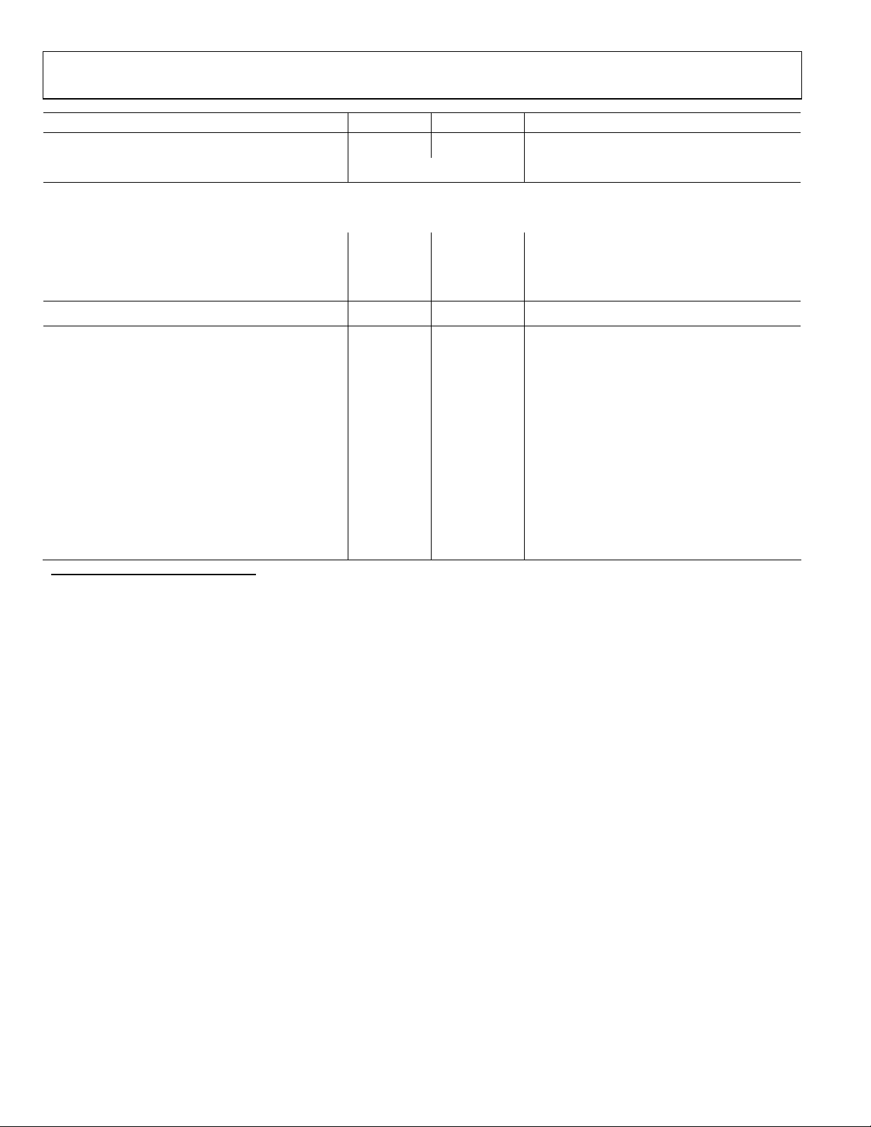
3 MSPS,12-/10-/8-Bit
Preliminary Technical Data
FEATURES
Fast throughput rate: 3 MSPS
Specified for VDD of 2.35 V to 3.6 V
Low power:
13.5 mW max at 3 MSPS with 3 V supplies
TBD mW typ at 1.5 MSPS with 3 V supplies
Wide input bandwidth:
70 dB SNR at 1 MHz input frequency
Flexible power/serial clock speed management
No pipeline delays
High speed serial interface
SPI®/QSPI™/MICROWIRE™/DSP compatible
Power-down mode: 1 µA max
6-lead TSOT package
8-lead MSOP package
AD7476 and AD7476A pin compatible
APPLICATIONS
Battery-powered systems
Personal digital assistants
Medical instruments
Mobile communications
Instrumentation and control systems
Data acquisition systems
High speed modems
Optical sensors
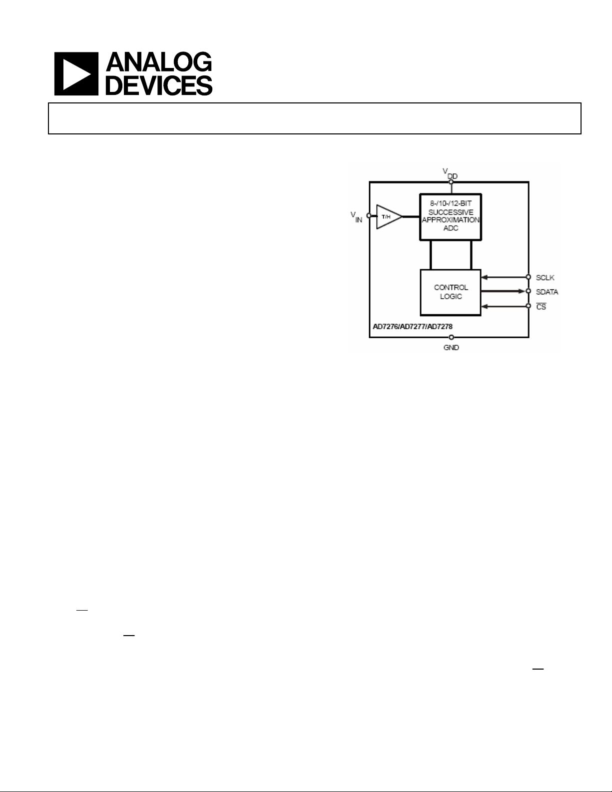
GENERAL DESCRIPTION
The AD7276/AD7277/AD7278 are 12-bit, 10-bit and 8-bit, high
speed, low power, successive-approximation ADCs respectively.
The parts operate from a single 2.35V to 3.6 V power supply
and feature throughput rates up to 3 MSPS. The parts contain a
low-noise, wide bandwidth track/hold amplifier which can
handle input frequencies in excess of TBD MHz.
The conversion process and data acquisition are controlled
CS
using
with microprocessors or DSPs. The input signal is sampled on
the falling edge of
point. There are no pipeline delays associated with the part.
The AD7276/AD7277/AD7278 use advanced design techniques
to achieve very low power dissipation at high throughput rates.
and the serial clock, allowing the devices to interface
CS
and the conversion is also initiated at this
ADCs in 6-Lead TSOT
AD7276/AD7277/AD7278
FUNCTIONAL BLOCK DIAGRAM
Figure 1.
The reference for the part is taken internally from VDD. This
allows the widest dynamic input range to the ADC. Thus the
analog input range for the part is 0 to V
is determined by the SCLK.
PRODUCT HIGHLIGHTS
1. 3 MSPS ADCs in a 6-lead TSOT package.
2. AD7476/77/78 and AD7476A/77A/78A pin compatible.
3. High Throughput with Low Power Consumption.
4. Flexible Power/Serial Clock Speed Management.
The conversion rate is determined by the serial clock
allowing the conversion time to be reduced through the serial
clock speed increase. This allows the average power
consumption to be reduced when a power-down mode is
used while not converting. The part also features a powerdown mode to maximize power efficiency at lower
throughput rates. Current consumption is 1 µA max when in
Power-Down mode.
5. Reference derived from the power supply.
6. No Pipeline Delay.
The parts feature a standard successive-approximation ADC
with accurate control of the sampling instant via a
and once-off conversion control.
. The conversion rate
DD
CS
input
Rev. PrG
Information furnished by Analog Devices is believed to be accurate and reliable.
However, no responsibility is assumed by Analog Devices for its use, nor for any
infringements of patents or other rights of third parties that may result from its use.
Specifications subject to change without notice. No license is granted by implication
or otherwise under any patent or patent rights of Analog Devices. Trademarks and
registered trademarks are the property of their respective owners.
One Technology Way, P.O. Box 9106, Norwood, MA 02062-9106, U.S.A.
Tel: 781.329.4700 www.analog.com
Fax: 781.326.8703 © 2005 Analog Devices, Inc. All rights reserved.

Preliminary Technical Data AD7276/AD7277/AD7278
TABLE OF CONTENTS
AD7278—Specifications.................................................................. 3
AD7277—Specifications.................................................................. 5
AD7276—Specifications.................................................................. 7
Timing Specifications....................................................................... 9
Timing Examples........................................................................ 10
Absolute Maximum Ratings.......................................................... 11
ESD Caution................................................................................ 11
Pin Configurations and Function Descriptions......................... 12
Terminology................................................................................ 13
Performance Curves....................................................................... 14
Dynamic Performance curves .................................................. 14
DC Accuracy Curves ................................................................. 14
Power Requirements Curves..................................................... 14
REVISION HISTORY
Typical Performance Characteristics........................................... 15
Theory of Operation ......................................................................17
Circuit Information.................................................................... 17
Converter Operation.................................................................. 17
ADC Transfer Function............................................................. 17
Typical Connection Diagram ................................................... 17
Modes of Operation................................................................... 19
Power Versus Throughput Rate................................................ 22
Serial Interface ................................................................................ 23
AD7278 in a 10 SCLK’s cycle Serial Interface ........................ 24
Outline Dimensions....................................................................... 25
Ordering Guide .......................................................................... 25
Revision PrF: Preliminary Version
Rev. PrG | Page 2 of 25
Preliminary Technical Data AD7276/AD7277/AD7278
AD7278—SPECIFICATIONS
VDD = +2.35 V to +3.6 V, f
= 52 MHz, f
SCLK
= 3 MSPS, TA = T
SAMPLE
MIN
to T
, unless otherwise noted.
MAX
Table 1.
Parameter B Grade1 Unit Test Conditions/Comments
DYNAMIC PERFORMANCE fIN = 1MHz Sine Wave
Signal-to-Noise + Distortion (SINAD)2 49 dB min
Total Harmonic Distortion (THD)2 −65 dB max
Peak Harmonic or Spurious Noise (SFDR)2 −65 dB max
Intermodulation Distortion (IMD)2
Second Order Terms −76 dB typ fa = TBD kHz, fb = TBD kHz
Third Order Terms −76 dB typ fa = TBD kHz, fb = TBD kHz
Aperture Delay TBD ns typ
Aperture Jitter TBD ps typ
Full Power Bandwidth TBD MHz typ @ 3 dB
Full Power Bandwidth TBD MHz typ @ 0.1dB
DC ACCURACY
Resolution 8 Bits
Integral Nonlinearity2 ±0.3 LSB max
Differential Nonlinearity2 ±0.3 LSB max Guaranteed No Missed Codes to 8 Bits
Offset Error2 ±0.5 LSB max
±TBD LSB typ
Gain Error2 ±0.5 LSB max
±TBD LSB typ
Total Unadjusted Error (TUE)2 ±TBD LSB max
ANALOG INPUT
Input Voltage Ranges 0 to VDD Volts
DC Leakage Current ±0.5 µA max
Input Capacitance TBD pF typ
LOGIC INPUTS
Input High Voltage, V
1.7 V min 2.35V ≤ Vdd ≤ 2.7V
INH
2 V min 2.7V < Vdd ≤ 3.6V
Input Low Voltage, V
0.7 V max 2.35V ≤ Vdd< 2.7V
INL
0.8 V max 2.7V ≤ Vdd ≤ 3.6V
Input Current, IIN, SCLK Pin ±0.5 µA max Typically TBD nA, VIN = 0 V or VDD
Input Current, IIN, CS Pin
Input Capacitance, C
3
10 pF max
IN
± 1 µA max
LOGIC OUTPUTS
Output High Voltage, VOH V
Output Low Voltage, VOL 0.2 V max I
– 0.2 V min I
DD
= 200 µA,VDD = 2.35 V to 3.6V
SOURCE
= 200µA
SINK
Floating-State Leakage Current ±1 µA ma
Floating-State Output Capacitance3 10 pF max
Output Coding Straight (Natural) Binary
CONVERSION RATE
Conversion Time 192 ns max 10 SCLK Cycles with SCLK at 52 MHz
Track/Hold Acquisition Time2 50 ns max
Throughput Rate 3 MSPS max
POWER REQUIREMENTS
Rev. PrG | Page 3 of 25
AD7276/AD7277/AD7278 Preliminary Technical Data
Parameter B Grade1 Unit Test Conditions/Comments
VDD 2.35/3.6 Vmin/max
IDD Digital I/Ps= 0V or VDD
Normal Mode(Static) 2.5 mA typ VDD = 2.35V to 3.6V, SCLK On or Off
Normal Mode (Operational) 4.5 mA max VDD = 2.35V to 3.6V, f
Full Power-Down Mode (Static) 1 µA max SCLK On or Off, typically TBD nA
Power Dissipation4
Normal Mode (Operational)
13.5 mW max VDD = 3V, f
SAMPLE
= 3 MSPS
Partial Power Down Mode
Full Power-Down 3 µW max VDD = 3V
1
Temperature range from −40°C to +85°C.
2
See Terminology.
3
Guaranteed by characterization.
4
See Power Versus Throughput Rate section.
Specifications subject to change without notice.
SAMPLE
= 3MSPS
Rev. PrG | Page 4 of 25
Preliminary Technical Data AD7276/AD7277/AD7278
AD7277—SPECIFICATIONS
VDD =+2.35 V to +3.6 V, f
= 52 MHz, f
SCLK
= 3 MSPS, TA = T
SAMPLE
MIN
to T
, unless otherwise noted.
MAX
Table 2.
Parameter B Grade
DYNAMIC PERFORMANCE
Signal-to-Noise + Distortion (SINAD)
Total Harmonic Distortion (THD)
2
Peak Harmonic or Spurious Noise (SFDR)
Intermodulation Distortion (IMD)
2
2
61 dB min
−73 dB max
2
−74 dB max
1
Unit Test Conditions/Comments
fIN = 1 MHz Sine Wave
Second Order Terms −82 dB typ fa = TBD kHz, fb = TBD kHz
Third Order Terms −82 dB typ fa = TBD kHz, fb = TBD kHz
Aperture Delay TBD ns typ
Aperture Jitter TBD ps typ
Full Power Bandwidth TBD MHz typ @ 3 dB
Full Power Bandwidth TBD MHz typ @ 0.1dB
DC ACCURACY
Resolution 10 Bits
Integral Nonlinearity
Differential Nonlinearity
Offset Error
2
±1 LSB max
2
±0.5 LSB max
2
±0.5 LSB max Guaranteed No Missed Codes to 10 Bits
Gain Error
2
±1 LSB max
Total Unadjusted Error (TUE)
ANALOG INPUT
Input Voltage Ranges 0 to V
DC Leakage Current ±0.5 µA max
Input Capacitance TBD pF typ
LOGIC INPUTS
Input High Voltage, V
2
±TBD LSB max
1.7 V min 2.35V ≤ Vdd ≤ 2.7V
INH
Input Low Voltage, V
0.7 V max 2.35V ≤ Vdd< 2.7V
INL
±TBD LSB typ
±TBD LSB typ
Volts
DD
2 V min 2.7V <Vdd ≤ 3.6V
0.8 V max 2.7V ≤ Vdd ≤ 3.6V
Input Current, IIN, SCLK Pin ±0.5 µA max Typically TBD nA, VIN = 0 V or V
Input Current, IIN, CS Pin
Input Capacitance, C
3
10 pF max
IN
LOGIC OUTPUTS
Output High Voltage, V
Output Low Voltage, V
V
OH
0.2 V max I
OL
Floating-State Leakage Current ±1 µA max
± 1 µA max
– 0.2 V min I
DD
= 200 µA,VDD= 2.35 V to 3.6 V
SOURCE
= 200µA
SINK
DD
Rev. PrG | Page 5 of 25
AD7276/AD7277/AD7278 Preliminary Technical Data
Parameter B Grade
Floating-State Output Capacitance
3
10 pF max
Output Coding Straight (Natural) Binary
CONVERSION RATE
1
Unit Test Conditions/Comments
Conversion Time 230 ns max 12 SCLK cycles with SCLK at 52 MHz
Track/Hold Acquisition Time
Throughput Rate 3 MSPS max
POWER REQUIREMENTS
V
2.35/3.6 V min/max
DD
I
DD
2
50 ns max
Digital I/Ps 0V or V
DD
Normal Mode(Static) 2.5 mA typ VDD = 2.35V to 3.6V, SCLK On or Off
Normal Mode (Operational) 4.5 mA max VDD = 2.35V to 3.6V, f
SAMPLE
= 3MSPS
Full Power-Down Mode(Static) 1 µA max SCLK On or Off, typically TBD nA
Full Power-Down Mode(Dynamic) TBD mA typ VDD = 3V, f
Power Dissipation
Normal Mode (Operational)
4
13.5 mW max VDD = 3V, f
SAMPLE
SAMPLE
= 1 MSPS
= 3 MSPS
Partial Power-Down
Full Power-Down 3 µW max VDD =3V
1
Temperature range from −40°C to +85°C.
2
See Terminology.
3
Guaranteed by Characterization.
4
See Power Versus Throughput Rate section.
Specifications subject to change without notice.
Rev. PrG | Page 6 of 25
Preliminary Technical Data AD7276/AD7277/AD7278
AD7276—SPECIFICATIONS
VDD = +2.35 V to +3.6 V, f
= 52 MHz, f
SCLK
= 3 MSPS, TA = T
SAMPLE
MIN
to T
, unless otherwise noted.
MAX
Table 3.
Parameter B Grade1 Units Test Conditions/Comments
DYNAMIC PERFORMANCE fIN = 1 MHz Sine Wave
Signal-to-Noise + Distortion (SINAD)2 70 dB min
Signal-to-Noise Ratio (SNR) 71 dB min
Total Harmonic Distortion (THD)2 −80 dB max
Peak Harmonic or Spurious Noise (SFDR)2 −82 dB max
Intermodulation Distortion (IMD)2
Second Order Terms −84 dB typ Fa = TBD kHz, fb = TBD kHz
Third Order Term −84 dB typ Fa = TBD kHz, fb = TBD kHz
Aperture Delay TBD ns typ
Aperture Jitter TBD ps typ
Full Power Bandwidth TBD MHz typ @ 3 dB
Full Power Bandwidth TBD MHz typ @ 0.1dB
DC ACCURACY
Resolution 12 Bits
Integral Nonlinearity2 ±1 LSB max
Differential Nonlinearity2 ±1 LSB max Guaranteed No Missed Codes to 12 Bits
Offset Error2 ±TBD LSB max
Gain Error2 ±TBD LSB max
Total Unadjusted Error (TUE)2 ±TBD LSB max
ANALOG INPUT
Input Voltage Ranges 0 to VDD Volts
DC Leakage Current ±0.5 µA max
Input Capacitance TBD pF typ
LOGIC INPUTS
Input High Voltage, V
1.7 V min 2.35V ≤ Vdd ≤ 2.7V
INH
2 V min 2.7V < Vdd ≤ 3.6V
Input Low Voltage, V
0.7 V max 2.35V ≤ Vdd< 2.7V
INL
0.8 V max 2.7V ≤ Vdd ≤ 3.6V
Input Current, IIN,SCLK Pin ±0.5 µA max Typically TBDnA, VIN = 0 V or VDD
Input Current, IIN, CS Pin
Input Capacitance, C
3
10 pF max
IN
± 1 µA max
LOGIC OUTPUTS
Output High Voltage, VOH V
Output Low Voltage, VOL 0.2 V max I
–0.2 V min I
DD
= 200 µA;VDD = 2.35 V to 3.6V
SOURCE
=200 µA
SINK
Floating-State Leakage Current ±1 µA max
Floating-State Output Capacitance3 10 pF max
Output Coding Straight (Natural) Binary
CONVERSION RATE
Conversion Time 270 ns max 14 SCLK Cycles with SCLK at 52 MHz
Track/Hold Acquisition Time2 50 ns max
Throughput Rate 3 MSPS max See Serial Interface Section
POWER REQUIREMENTS
VDD 2.35/3.6 V min/max
Rev. PrG | Page 7 of 25
AD7276/AD7277/AD7278 Preliminary Technical Data
Parameter B Grade1 Units Test Conditions/Comments
IDD Digital I/Ps 0V or VDD
Normal Mode(Static) 2.5 mA typ VDD = 2.35V to 3.6V, SCLK On or Off
Normal Mode (Operational) 4.5 mA max VDD = 2.35V to 3.6V, f
Full Power-Down Mode(Static) 1 µA max SCLK On or Off, typically TBD nA
Full Power-Down Mode(Dynamic) TBD mA typ VDD = 3V, f
SAMPLE
= 1MSPS
Power Dissipation4
Normal Mode (Operational)
13.5 mW max VDD = 3V, f
SAMPLE
= 3MSPS
Partial Power-Down
Full Power-Down 3 µW max VDD =3V
1
Temperature range from −40°C to +85°C.
2
See Terminology.
3
Guaranteed by Characterization.
4
See Power Versus Throughput Rate section.
Specifications subject to change without notice.
SAMPLE
= 3MSPS
Rev. PrG | Page 8 of 25

Preliminary Technical Data AD7276/AD7277/AD7278
TIMING SPECIFICATIONS
VDD = +2.35 V to +3.6 V; TA = T
Guaranteed by characterization. All input signals are specified with tr = tf = 5 ns (10% to 90% of V
MIN
to T
, unless otherwise noted.
MAX
) and timed from a voltage level of
DD
1.6 V.
Table 4.
, T
Limit at T
Parameter
1
f
20 KHz min2
SCLK
AD7276/AD7277/AD7278 Unit Description
MIN
MAX
52 MHz max
t
CONVERT
14 × t
AD7276
SCLK
12 × tSCLK AD7277
10 × t
t
TBD ns min Minimum Quiet Time required between Bus Relinquish and start of
QUIET
AD7278
SCLK
Next Conversion
t1 10 ns min
t2 TBD ns min
3
t
TBD ns max
3
3
t
TBD ns max Data Access Time After SCLK Falling Edge
4
t5 0.4t
t6 0.4t
3
t
TBD ns min SCLK to Data Valid Hold Time
7
4
t
TBD ns max SCLK Falling Edge to SDATA Three-State
8
ns min SCLK Low Pulse Width
SCLK
ns min SCLK High Pulse Width
SCLK
Minimum
CS
Delay from
CS
Pulse Width
to SCLK Setup Time
CS
Until SDATA Three-State Disabled
TBD ns min SCLK Falling Edge to SDATA Three-State
5
t
2 µs max Power Up Time from Full Power-down
power-up
1
Mark/Space ratio for the SCLK input is 40/60 to 60/40.
2
Minimum f
3
The time required for the output to cross the Vih or Vil voltage.
4
t8 is derived from the measured time taken by the data outputs to change 0.5 V. The measured number is then extrapolated back to remove the effects of charging or
discharging the 25 pF capacitor. This means that the time, t8, quoted in the timing characteristics is the true bus relinquish time of the part and is independent of the bus
loading.
5
See Power-up Time section
Specifications subject to change without notice.
at which specifications are guaranteed.
sclk
Figure 2. Access time after SCLK falling edge
Figure 3. Hold time after SCLK falling edge
Figure 4. SCLK falling edge SDATA Three-State
Rev. PrG | Page 9 of 25

AD7276/AD7277/AD7278 Preliminary Technical Data
TIMING EXAMPLES
Figure 5 and Figure 6 show some of the timing parameters from
the Timing Specifications section.
Timing Example 1
From Figure 6, having f
3MSPS, gives a cycle time of t
With t
= TBD ns min, this leaves t
2
ns satisfies the requirement of TBD ns for t
that, t
comprises of 2.5(1/f
ACQ
ns max. This allows a value of TBD ns for t
minimum requirement of TBD ns.
= 52 MHz and a throughput of
SCLK
+ 12.5(1/f
2
ACQ
) + t8 + t
SCLK
) + t
SCLK
ACQ
to be TBD ns. This TBD
. Figure 6 shows
ACQ
, where t8 = TBD
QUIET
satisfying the
QUIET
= 333 ns.
Timing Example 2
Having f
cycle time of t
min, this leaves t
= 20 MHz and a throughput of 1.5 MSPS, gives a
SCLK
+ 12.5(1/f
2
ACQ
SCLK
to be TBD ns. This TBD ns satisfies the
requirement of TBD ns for t
of 2.5(1/f
SCLK
) + t8 + t
values of TBD ns for t
, where t8 = TBD ns max. This allows a
QUIET
QUIET
of TBD ns.
) + t
= 666 ns. With t2 = TBD ns
ACQ
. From Figure 6, t
ACQ
comprises
ACQ
satisfying the minimum requirement
Figure 5. AD7276 Serial Interface Timing Diagram
Figure 6. Serial Interface Timing Example
Rev. PrG | Page 10 of 25

Preliminary Technical Data AD7276/AD7277/AD7278
ABSOLUTE MAXIMUM RATINGS
TA = +25°C unless otherwise noted.
Table 5.
Parameters Ratings
VDD to GND −0.3 V to TBD V
Analog Input Voltage to GND
Digital Input Voltage to GND −0.3 V to TBD V
Digital Output Voltage to GND
Input Current to Any Pin Except Supplies1 ±10 mA
Operating Temperature Range
Commercial (B Grade) −40°C to +85°C
Storage Temperature Range −65°C to +150°C
Junction Temperature 150°C
6-lead TSOT Package
θJA Thermal Impedance TBD°C/W
θJC Thermal Impedance TBD°C/W
8-lead MSOP Package
θJA Thermal Impedance 205.9°C/W
θJC Thermal Impedance 43.74°C/W
Lead Temperature Soldering
Reflow (10– 30 sec) +TBD°C
ESD TBD KV
−0.3 V to V
V
−0.3 V to V
V
DD
DD
+ 0.3
+ 0.3
Stresses above those listed under Absolute Maximum Ratings
may cause permanent damage to the device. This is a stress
rating only and functional operation of the device at these or
any other condition s above those indicated in the operational
section of this specification is not implied. Exposure to absolute
maximum rating conditions for extended periods may affect
device reliability.
1
Transient currents of up to 100 mA will not cause SCR latch up.
ESD CAUTION
ESD (electrostatic discharge) sensitive device. Electrostatic charges as high as 4000 V readily accumulate on the
human body and test equipment and can discharge without detection. Although this product features proprietary
ESD protection circuitry, permanent damage may occur on devices subjected to high energy electrostatic
discharges. Therefore, proper ESD precautions are recommended to avoid performance degradation or loss of
functionality.
Rev. PrG | Page 11 of 25

AD7276/AD7277/AD7278 Preliminary Technical Data
PIN CONFIGURATIONS AND FUNCTION DESCRIPTIONS
Figure 7. 6-Lead TSOT Pin Configuration
Table 6. Pin Function Descriptions
Pin No.
(TSOT)
1 1 V
2 7 GND
Pin No.
(MSOP) Mnemonic Function
Power Supply Input. The V
DD
Analog Ground. Ground reference point for all circuitry on the AD7276/AD7277/AD7278. All analog
input signals should be referred to this GND voltage.
3 8 V
4 6 SCLK
Analog Input. Single-ended analog input channel. The input range is 0 to V
IN
Serial Clock. Logic input. SCLK provides the serial clock for accessing data from the part. This clock input
is also used as the clock source for the AD7276/AD7277/AD7278's conversion process.
5 2 SDATA
Data Out. Logic Output. The conversion result from the AD7276/AD7277/AD7278 is pro-vided on this
output as a serial data stream. The bits are clocked out on the falling edge of the SCLK input. The data
stream from the AD7276 consists of two leading zeros followed by the 12 bits of conversion data followed
by two trailing zeros, which is provided MSB first. The data stream from the AD7277 consists of two
leading zeros followed by the 10 bits of conversion data followed by four trailing zeros, which is provided
MSB first. The data stream from the AD7278 consists of two leading zeros followed by the 8 bits of
conversion data followed by six trailing zeros, which is provided MSB first.
6 3
CS
Chip Select. Active low logic input. This input provides the dual function of initiating conversion on the
AD7276/AD7277/AD7278 and also frames the serial data transfer.
range for the AD7276/AD7277/AD7278 is from +2.35V to +3.6V.
DD
Figure 8. 8-Lead MSOP Pin Configuration
.
DD
Rev. PrG | Page 12 of 25

Preliminary Technical Data AD7276/AD7277/AD7278
TERMINOLOGY
Integral Nonlinearity
This is the maximum deviation from a straight line passing
through the endpoints of the ADC transfer function. For the
AD7276/AD7277/AD7278, the endpoints of the transfer
function are zero scale, a point 1/2 LSB below the first code
transition, and full scale, a point 1/2 LSB above the last code
transition.
Differential Nonlinearity
This is the difference between the measured and the ideal 1 LSB
change between any two adjacent codes in the ADC.
Offset Error
This is the deviation of the first code transition (00 . . . 000) to
(00 . . . 001) from the ideal, i.e, AGND + 0.5 LSB.
Gain Error
This is the deviation of the last code transition (111 . . . 110) to
(111 . . . 111) from the ideal, i.e, V
− 1.5LSB after the offset
REF
error has been adjusted out.
Tot a l U n ad ju s te d E rr o r
This is a comprehensive specification which includes gain,
linearity and offset errors.
Track-and-Hold Acquisition Time
The Track/Hold acquisition time is the time required for the
output of the track/hold amplifier to reach its final value, within
±0.5 LSB, after the end of conversion. See Serial Interface
section for more details.
Signal-to-Noise Ratio (SNR)
This is the measured ratio of signal to noise at the output to the
A/D converter. The signal is the rms value of the sine wave
input. Noise is the rms quantization error within the Nyquist
bandwitdh (fs/2). The rms value of a sine wave is one half its
peak to peak value divided by √2 and the rms value for the
quantization noise is q/√12. The ratio is dependant on the
number of quantization levels in the digitization process; the
more levels, the smaller the quantization noise. For an ideal Nbit converter, the SNR is defined as:
dB761N026SNR .. +
Thus for a 12-bit converter this is 74 dB, for a 10-bit converter it
is 62dB and for an 8-bit converter it is 50dB.
sine wave and noise is the rms sum of all nonfundamentals
signals up to half the sampling frequency (fs/2), including
harmonics but excluding dc.
Total Harmonic Distortion
Total harmonic distortion (THD) is the ratio of the rms sum of
harmonics to the fundamental. It is defined as:
2
20dBTHD
()
where V
V
is the rms amplitude of the fundamental and V2, V3,
1
, V5 and V6 are the rms amplitudes of the second through the
4
2
log
4
3
V
1
VVVVV
++++
6
5
2
2
2
2
sixth harmonics.
Peak Harmonic or Spurious Noise
Peak harmonic or spurious noise is defined as the ratio of the
rms value of the next largest component in the ADC output
spectrum (up to f
/2 and excluding dc) to the rms value of the
S
fundamental. Normally, the value of this specification is
determined by the largest harmonic in the spectrum, but for
ADCs where the harmonics are buried in the noise floor, it will
be a noise peak.
Intermodulation Distortion
With inputs consisting of sine waves at two frequencies, fa and
fb, any active device with nonlinearities will create distortion
products at sum and difference frequencies of mfa ± nfb where
m, n = 0, 1, 2, 3, etc. Intermodulation distortion terms are those
for which neither m nor n are equal to zero. For example, the
second order terms include (fa + fb) and (fa − fb), while the
third order terms include (2fa + fb), (2fa − fb), (fa + 2fb) and (fa
− 2fb).
The AD7276/AD7277/AD7278 are tested using the CCIF
standard where two input frequencies are used (see fa and fb in
the specification page). In this case, the second order terms are
usually distanced in frequency from the original sine waves
while the third order terms are usually at a frequency close to
the input frequencies. As a result, the second and third order
terms are specified separately. The calculation of the
intermodulation distortion is as per the THD specification
where it is the ratio of the rms sum of the individual distortion
products to the rms amplitude of the sum of the fundamentals
expressed in dBs.
Practically, though, various error sources in the ADC cause the
measured SNR to be less than the theoretical value. These errors
occur due to integral and differential nonlinearities, internal AC
noise sources, etc.
Signal-to-Noise + Distortion Ratio (SINAD)
This is the measured ratio of signal to (noise + distortion) at the
output of the A/D converter. The signal is the rms value of the
Rev. PrG | Page 13 of 25
Aperture Delay
This is the measured interval between the leading edge of the
sampling clock and the point at which the ADC actually takes
the sample.
Aperture Jitter
This is the sample-to-sample variation in the effective point in
time at which the sample is taken.

AD7276/AD7277/AD7278 Preliminary Technical Data
PERFORMANCE CURVES
DYNAMIC PERFORMANCE CURVES
Figure 9, Figure 10 and Figure 11 show typical FFT plots for the
AD7276, AD7277 and AD7278 respectively, at 3 MSPS sample
rate and TBD KHz input tone.
Figure 12 shows the Signal-to-Noise + Distortion Ratio
performance versus Input frequency for various supply voltages
while sampling at 3 MSPS with a SCLK frequency of 52 MHz
for the AD7276.
Figure 13 shows the Signal to Noise Ratio (SNR) performance
versus Input frequency for various supply voltages while
sampling at 3 MSPS with a SCLK frequency of 52 MHz for the
AD7276.
Figure 14 shows a graph of the Total Harmonic Distortion
versus Analog input signal frequency for various supply
voltages while sampling at 3 MSPS with a SCLK frequency of 52
MHz for the AD7276.
Figure 15 shows a graph of the Total Harmonic Distortion
versus Analog input frequency for different source impedances
when using a supply voltage of TBD V, SCLK frequency of 52
MHz and sampling at a rate of 3 MSPS for the AD7276. See
Analog Input section.
DC ACCURACY CURVES
Figure 16 and Figure 17 show typical INL and DNL
performance for the AD7276.
POWER REQUIREMENTS CURVES
Figure 18 shows Maximum current versus Supply voltage for
the AD7276 with different SCLK frequencies. See also Power
versus Throughput Rate section.
Rev. PrG | Page 14 of 25

Preliminary Technical Data AD7276/AD7277/AD7278
TYPICAL PERFORMANCE CHARACTERISTICS
Figure 9. AD7276 Dynamic performance at 3 MSPS
Figure 10. AD7277 Dynamic performance at 3 MSPS
Figure 12. AD7276 SINAD vs Analog Input Frequency at 3 MSPS
for various Supply Voltages
Figure 13. AD7276 SNR vs Analog Input Frequency at 3 MSPS
for various Supply Voltages
Figure 11. AD7278 Dynamic performance at 3 MSPS
Rev. PrG | Page 15 of 25
Figure 14. THD vs. Analog Input Frequency at 3 MSPS
for various Supply Voltages

AD7276/AD7277/AD7278 Preliminary Technical Data
Figure 15. THD vs. Analog Input Frequency for various Supply Voltages
Figure 16. AD7276 INL performance
Figure 17. AD7276 DNL performance
Figure 18. Maximum current vs Supply voltage
for different SCLK frequencies
Rev. PrG | Page 16 of 25

Preliminary Technical Data AD7276/AD7277/AD7278
THEORY OF OPERATION
CIRCUIT INFORMATION
The AD7276/AD7277/AD7278 are fast, micropower, 12-/10-/8Bit, single supply, A/D converters respectively. The parts can be
operated from a +2.35V to +3.6V supply. When operated from
any supply voltage within this range, the AD7276/AD7277/
AD7278 are capable of throughput rates of 3 MSPS when
provided with a 52 MHz clock.
The AD7276/AD7277/AD7278 provide the user with an onchip track/hold, A/D converter, and a serial interface housed in
a tiny 6-lead TSOT or 8-lead MSOP package, which offers the
user considerable space saving advantages over alternative
solutions. The serial clock input accesses data from the part but
also provides the clock source for the successive-approximation
A/D converter. The analog input range is 0 to V
reference is not required for the ADC and neither is there a
reference onchip. The reference for the AD7276/AD7277/
AD7278 is derived from the power supply and thus gives the
widest dynamic input range.
The AD7276/AD7277/AD7278 also feature a power down
option to allow power saving between conversions. The PowerDown feature is implemented across the standard serial
interface as described in the Modes of Operation section.
. An external
DD
Figure 21 shows the ADC transfer function.
Figure 20. ADC Conversion Phase
ADC TRANSFER FUNCTION
The output coding of the AD7276/AD7277/AD7278 is straight
binary. The designed code transitions occur midway between
successive integer LSB values, i.e, 0.5LSB, 1.5LSBs, etc. The LSB
size is V
V
DD
the AD7276/AD7277/AD7278 is shown in Figure 21.
/4096 for the AD7276, VDD/1024 for the AD7277 and
DD
/256 for the AD7278. The ideal transfer characteristic for
CONVERTER OPERATION
The AD7276/AD7277/AD7278 is a successive approximation
analog-to-digital converter based around a charge
redistribution DAC. Figure 19 and Figure 20 show simplified
schematics of the ADC. Figure 19 shows the ADC during its
acquisition phase. SW2 is closed and SW1 is in position A, the
comparator is held in a balanced condition and the sampling
capacitor acquires the signal on V
Figure 19. ADC Acquisition Phase
When the ADC starts a conversion, see Figure 20, SW2 will
open and SW1 will move to position B causing the comparator
to become unbalanced. The Control Logic and the Charge
Redistribution DAC are used to add and subtract fixed amounts
of charge from the sampling capacitor to bring the comparator
back into a balanced condition. When the comparator is
rebalanced the conversion is complete. The Control Logic
generates the ADC output code.
.
IN
Figure 21. AD7276/AD7277/AD7278 Transfer Characteristics
TYPICAL CONNECTION DIAGRAM
Figure 22 shows a typical connection diagram for the
AD7276/AD7277/AD7278. V
and as such V
should be well decoupled. This provides an
DD
analog input range of 0V to V
in a 16-bit word with two leading zeros followed by the 12-bit,
10-bit or 8-bit result. The 12-bit result from the AD7276 will be
followed by two trailing zeros and the 10-bit and 8-bit result
from the AD7277 and AD7278 will be followed by four and six
trailing zeros respectively.
Alternatively, because the supply current required by the
AD7276/AD7277/AD7278 is so low, a precision reference can
be used as the supply source to the AD7276/AD7277/AD7278.
A REF19x voltage reference (REF193 for 3V) can be used to
supply the required voltage to the ADC-see Figure 22. This
configuration is especially useful if the power supply is quite
noisy or if the system supply voltages are at some value other
is taken internally from VDD
REF
. The conversion result is output
DD
Rev. PrG | Page 17 of 25

AD7276/AD7277/AD7278 Preliminary Technical Data
than 3V (e.g. 5V or 15V). The REF19x will output a steady
voltage to the AD7276/7277/7278. If the low dropout REF193 is
used, the current it needs to supply to the AD7276/AD7277/
AD7278 is typically TBD mA. When the ADC is converting at a
rate of 3 MSPS the REF193 will need to supply a maximum of
TBD mA to the AD7276/AD7277/AD7278. The load regulation
of the REF193 is typically 10 ppm/mA (REF193, V
= 5V),
S
which results in an error of TBD ppm (TBD µV) for the TBD
mA drawn from it. This corresponds to a TBD LSB error for the
AD7276 with V
= 3V from the REF193, a TBD LSB error for
DD
the AD7277, and a TBD LSB error for the AD7278. For
applications where power consumption is of concern, the
Power-Down mode of the ADC and the sleep mode of the
REF19x reference should be used to improve power
performance. See Modes of Operation section.
part. The capacitor C1 in Figure 23 is typically about 4pF and
can primarily be attributed to pin capacitance. The resistor R1 is
a lumped component made up of the on resistance of a switch.
This resistor is typically about TBDΩ. The capacitor C2 is the
ADC sampling capacitor and has a capacitance of TBD pF
typically. For ac applications, removing high frequency
components from the analog input signal is recommended by
use of a bandpass filter on the relevant analog input pin. In
applications where harmonic distortion and signal to noise ratio
are critical, the analog input should be driven from a low
impedance source. Large source impedances will significantly
affect the ac performance of the ADC. This may necessitate the
use of an input buffer amplifier. The choice of the op-amp will
be a function of the particular application.
Figure 22. REF193 as Power Supply to AD7276/AD7277/AD7278
Table 7 provides some typical performance data with various
references used as a V
source under the same set-up
DD
conditions.
Table 7. AD7276 performance for various Voltage
References IC
Reference Tied To
V
DD
AD780@3V TBD dB
ADR423 TBD dB
AD780@2.5V TBD dB
REF192 TBD dB
ADR421 TBD dB
ADR291 TBD dB
AD7276 SNR Performance TBD kHz
Input
Analog Input
Figure 23 shows an equivalent circuit of the analog input
structure of the AD7276/AD7277/AD7278. The two diodes D1
and D2 provide ESD protection for the analog inputs. Care
must be taken to ensure that the analog input signal never
exceeds the supply rails by more than 300mV. This will cause
these diodes to become forward biased and start conducting
current into the substrate. 10mA is the maximum current these
diodes can conduct without causing irreversible damage to the
Figure 23. Equivalent Analog Input Circuit
Table 8 provides some typical performance data with various
op-amps used as the input buffer under the same set-up
conditions.
Table 8. AD7276 performance for various Input Buffers
Op-amp in the input
buffer
AD8510 TBD dB
AD8610 TBD dB
AD8038 TBD dB
AD8519 TBD dB
AD7276 SNR Performance TBD kHz
Input
When no amplifier is used to drive the analog input, the source
impedance should be limited to low values. The maximum
source impedance will depend on the amount of total harmonic
distortion (THD) that can be tolerated. The THD will increase
as the source impedance increases and performance will
degrade. Figure 15 shows a graph of the Total Harmonic
Distortion versus Analog input frequency for different source
impedances when using a supply voltage of TBD V and
sampling at a rate of 3 MSPS.
Digital Inputs
The digital inputs applied to the AD7276/AD7277/AD7278 are
not limited by the maximum ratings which limit the analog
inputs. Instead, the digitals inputs applied can go to TBDV and
Rev. PrG | Page 18 of 25

Preliminary Technical Data AD7276/AD7277/AD7278
are not restricted by the VDD + 0.3V limit as on the analog inputs.
For example, if the AD7276/AD7277/AD7278 were operated with a
V
of 3V then 5V logic levels could be used on the digital inputs.
DD
However, it is important to note that the data output on SDATA
will still have 3V logic levels when V
SCLK and
CS
not being restricted by the VDD + 0.3V limit is the
fact that power supply sequencing issues are avoided. If
= 3V. Another advantage of
DD
CS
or SCLK
are applied before VDD then there is no risk of latch-up as there
would be on the analog inputs if a signal greater than 0.3V was
applied prior to V
DD
.
Partial Power-Down Mode
This mode is intended for use in applications where slower
throughput rates are required; either the ADC is powered down
between each conversion, or a series of conversions may be
performed at a high throughput rate and then the ADC is powered
down for a relatively long duration between these bursts of several
conversions.
When the AD7276/AD7277/AD7278 is in Partial Power-Down, all
analog circuitry is powered down except the bias generation circuit.
MODES OF OPERATION
The mode of operation of the AD7276/AD7277/AD7278 is selected
by controlling the logic state of the
There are three possible modes of operation, Normal Mode, Partial
Power-Down Mode and Full Power-Down Mode . The point at
CS
which
is pulled high after the conversion has been initiated will
determine which power down mode ,if any,
AD7276/AD7277/AD7278 will enter. Similarly, if already in
power-down mode, then CS can control whether the device will
return to normal operation or remain in power-down. These
modes of operation are designed to provide flexible power
management options. These options can be chosen to optimize the
power dissipation/throughput rate ratio for different application
requirements.
Normal Mode
This mode is intended for fastest throughput rate performance as
the user does not have to worry about any power-up times with the
AD7276/AD7277/AD7278 remaining fully powered all the time.
Figure 24 shows the general diagram of the operation of the
AD7276/AD7277/AD7278 in this mode.
The conversion is initiated on the falling edge of
the Serial Interface section. To ensure the part remains fully
powered up at all times
CS
SCLK falling edges have elapsed after the falling edge of
brought high any time after the 10th SCLK falling edge, but before
th
the 16
SCLK falling edge, the part will remain powered up but the
conversion will be terminated and SDATA will go back into threestate.
For the AD7276 a minimum of 14 serial clock cycles are required to
complete the conversion and access the complete conversion result.
For the AD7277 and AD7278 a minimum of 12 and 10 serial clock
cycles are required to complete the conversion and access the
complete conversion result, respectively.
CS
may idle high until the next conversion or may idle low until CS
returns high sometime prior to the next conversion (effectively
idling CS low).
Once a data transfer is complete (SDATA has returned to threestate), another conversion can be initiated after the quiet time,
t
, has elapsed by bringing CS low again.
QUIET
CS
signal during a conversion.
CS
as described in
must remain low until at least 10th
CS
. If CS is
To enter partial power-down, the conversion process must be
interrupted by bringing
of SCLK and before the 10
Figure 25. Once
CS
high anywhere after the 2nd falling edge
th
falling edge of SCLK as shown in
CS
has been brought high in this window of
SCLKs, then the part will enter partial power-down and the
conversion that was initiated by the falling edge of
terminated and SDATA will go back into three-state. If
brought high before the 2
nd
SCLK falling edge, then the part will
CS
will be
CS
is
remain in Normal Mode and will not power-down. This will avoid
accidental power-down due to glitches on the CS line.
In order to exit this mode of operation and power the
AD7276/AD7277/AD7278 up again, a dummy conversion is
performed. On the falling edge of
up, and will continue to power up as long as
CS
the device will begin to power
CS
is held low until
after the falling edge of the 10th SCLK. The device will be fully
powered up once 16 SCLKs have elapsed and valid data will result
from the next conversion as shown in Figure . If CS is brought high
before the 2nd falling edge of SCLK, then the
AD7276/AD7277/AD7278 will go back into partial power-down
again. This avoids accidental power up due to glitches on the
line or an inadvertent burst of 8 SCLK cycles while
CS
CS
is low. So,
although the device may begin to power up on the falling edge of
CS
, it will power down again on the rising edge of CS as long as it
occurs before the 10th SCLK falling edge.
If the AD7276/77/78 is already in partial power-down mode and
CS
is brought high between the second and tenth falling edges of
SCLK, the device will enter full power-down mode. For more
information on the power-up times associated with partial powerdown in various configurations, see the Power-Up Times section.
Full Power Down Mode
This mode is intended for use in applications where throughput
rates slower than those in the partial power-down mode are
required, as power-up from a full power-down takes substantially
longer than that from partial power-down. This mode is more
suited to applications where a series of conversions performed at a
relatively high throughput rate would be followed by a long period
of inactivity and thus power-down.
When the AD7276/77/78 is in full power-down, all analog circuitry
is powered down. Full Power down will occur if
any time up to the 10
th
SCLK in the next cycle after partial power
CS
is brought high
down.
Rev. PrG | Page 19 of 25

AD7276/AD7277/AD7278 Preliminary Technical Data
The conversion process must be interrupted in a similar fashion by
CS
bringing
high anywhere after the second falling edge of SCLK
and before the tenth falling edge of SCLK. The device will enter
partial power-down at this point. To reach full power-down, the
next conversion cycle must be interrupted in the same way, as
shown in Figure 27. Once
CS
has been brought high in this
window of SCLKs, the part will power down completely. Note that
CS
it is not necessary to complete the 16 SCLKs once
has been
brought high to enter a power-down mode. Glitch protection is not
available when entering full power down.
To exit full power-down and power the AD7276/77/78 up again, a
dummy conversion is performed, as when powering up from
partial power-down. On the falling edge of
CS
, the device will
begin to power up and will continue to power up as long as CS is
held low until after the falling edge of the tenth SCLK. The powerup time required must elapse before a conversion can be initiated,
as shown in Figure 28. See the Power-Up Times section for the
power-up times associated with the AD7276/77/78.
Power Up Times
The AD7276/77/78 has two power-down modes, partial powerdown and full power-down, which are described in detail in the
Modes of Operation section. This section deals with the power-up
time required when coming out of either of these modes.
To power up from partial power-down mode, one cycle is required.
This means that with any frequency of SCLK up to 52MHz, one
dummy cycle will always be sufficient to allow the device to power
up from partial power down mode. Once the dummy cycle is
complete, the ADC will be fully powered up and the input signal
will be acquired properly. The quite time t
must still be allowed
QUIET
from the point where the bus goes back into three-state after the
dummy conversion, to the next falling edge of
CS
.
To power up from full power-down, approximately 2μs should be
allowed from the falling edge of CS, shown in Figure 28 as t
.
UP
It should also be noted that during power-up from partial powerdown, the track-and-hold, which was in hold mode while the part
was powered down, returns to track mode after the first SCLK edge
the part receives after the falling edge of CS. This is shown as point
A in Figure 26.
When power supplies are first applied to the AD7276/AD7277/
AD7278, the ADC may power up in either of the power-down
modes or in normal mode. Because of this, it is best to allow a
dummy cycle to elapse to ensure the part is full powered up before
attempting a valid conversion. Likewise, if the part is to be kept in
the partial power-down mode immediately after the supplies are
applied, two dummy cycles must be initiated. The first dummy
cycle must hold
Figure 25); in the second cycle,
CS
low until after the tenth SCLK falling edge (see
CS
must be brought high before the
tenth SCLK edge but after the second SCLK falling edge (see Figure
26).
Alternatively, if the part is to be placed in full power-down mode
when the supplies have been applied, three dummy cycles must be
initiated. The first dummy cycle must hold
CS
low until after the
tenth SCLK falling edge (see Figure 25); the second and third
dummy cycles place the part in full power-down (see Figure 27).
See also the Modes of Operation section
.
POWER
CS
SCLK
SDATA
Figure 24. Normal Mode Operation
2
1
Figure 25: Entering Partial Power Down Mode
Rev. PrG | Page 20 of 25
10
TRI-STATE
16

Preliminary Technical Data AD7276/AD7277/AD7278
CS
SCLK
SDATA
CS
SCLK
THE PART BEGINS
TO POWER UP
1
A
THE PART ENTERS
PARTIAL POWER DOWN
1
2
10
INVALID DATA
10
THE PART MAY BE FULLY
POWERED UP, SEE ‘POWER-
UP TIMES’ SECTION
16
1
Figure 26. Exiting Partial Power Down Mode
THE PART BEGINS
TO POWER UP
16
1
VALID DATA
THE PART ENTERS
FULL POWER DOWN
10
16
16
SDATA
CS
SCLK
SDATA
THE PART BEGINS
1
TO POWER UP
10
INVALID DATA
TRI-STATE
Figure27: Entering Full Power Down Mode
t
power up
16
Figure 28: Exiting Full Power Down Mode
INVALID DATAINVALID DATA
THE PART IS
FULLY POWERED UP
1
TRI-STATE
VALID DATA
16
Rev. PrG | Page 21 of 25

AD7276/AD7277/AD7278 Preliminary Technical Data
POWER VERSUS THROUGHPUT RATE
By using the Power-Down mode on the
AD7276/AD7277/AD7278 when not converting, the average
power consumption of the ADC decreases at lower throughput
rates. Figure shows how as the throughput rate is reduced, the
device remains in its Power-Down state longer and the average
power consumption over time drops accordingly. For example,
if the AD7276/AD7277/AD7278 is operated in a continuous
sampling mode with a throughput rate of 500KSPS and a SCLK
of 52MHz (V
Down mode between conversions, then the power consumption
is calculated as follows. The power dissipation during normal
operation is 13.5 mW (V
dummy cycle, i.e. 333ns, and the remaining conversion time is
another cycle, i.e. 333ns, then the AD7276/AD7277/AD7278
can be said to dissipate 13.5mW for 666ns during each
conversion cycle. If the throughput rate is 500KSPS, the cycle
time is 2µs and the average power dissipated during each cycle
is (666/2000) × (13.5 mW)= 4.5mW. Figure 29 shows the
Power vs. Throughput Rate when using the Power-Down mode
between conversions at 3V. The Power-Down mode is intended
= 3V), and the device is placed in the Power-
DD
= 3V). If the power up time is one
DD
for use with throughput rates of approximately TBD MSPS and
under as at higher sampling rates there is no power saving made
by using the Power-Down mode.
Figure 29. Power vs. Throughput
Rev. PrG | Page 22 of 25

Preliminary Technical Data AD7276/AD7277/AD7278
SERIAL INTERFACE
Figure , Figure , and Figure show the detailed timing diagram
for serial interfacing to the AD7276, AD7277 and AD7278
respectively. The serial clock provides the conversion clock and
also controls the transfer of information from the
AD7276/AD7277/AD7278 during conversion.
CS
signal initiates the data transfer and conversion process.
The
CS
The falling edge of
puts the track and hold into hold mode,
takes the bus out of three-state and the analog input is sampled
at this point. The conversion is also initiated at this point.
For the AD7276 the conversion will require 14 SCLK cycles to
complete. Once 13 SCLK falling edges have elapsed the track
and hold will go back into track on the next SCLK rising edge as
shown in Figure 30 at point B. If the rising edge of
CS
occurs
before 14 SCLKs have elapsed then the conversion will be
terminated and the SDATA line will go back into three-state. If
16 SCLKs are considered in the cycle, the last two bits will be
zeros and SDATA will return to three-state on the 16th SCLK
falling edge as shown in Figure .
For the AD7277 the conversion will require 12 SCLK cycles to
complete. Once 11 SCLK falling edges have elapsed, the track
and hold will go back into track on the next SCLK rising edge,
as shown in Figure at point B. If the rising edge of
CS
occurs
before 12 SCLKs have elapsed then the conversion will be
terminated and the SDATA line will go back into three-state. If
16 SCLKs are considered in the cycle, the AD7277 will clock out
four trailing zeros for the last four bits and SDATA will return
to three-state on the 16th SCLK falling edge, as shown in Figure
31.
For the AD7278 the conversion will require 10 SCLK cycles to
complete. Once 9 SCLK falling edges have elapsed, the track
and hold will go back into track on the next rising edge. If the
rising edge of
CS
occurs before 10 SCLKs have elapsed then the
part will enter Power-Down mode. If 16 SCLKs are considered
in the cycle, the AD7278 will clock out six trailing zeros for the
CS
t
convert
SCLK
SDATA
THREESTATE
t
2
1
t
3
Z
ZERO
2 LEADING
ZERO'S
2
DB11
3
DB10
t
6
4
5
t
t
4
DB9
Figure 30. AD7276 Serial Interface Timing Diagram
7
1/ THROUGHPUT
last six bits and SDATA will return to three-state on the 16th
SCLK falling edge, as shown in Figure .
If the user considers a 14 SCLKs cycle serial interface for the
CS
AD7276/AD7277/AD7278,
needs to be brought high after
the 14th SCLK falling edge, the last two trailing zeros will be
ignored and SDATA will go back into three-state. In this case,
the 3MSPS throughput could be achieved using a 45MHz clock
frequency.
CS
going low clocks out the first leading zero to be read in by
the microcontroller or DSP. The remaining data is then clocked
out by subsequent SCLK falling edges beginning with the 2nd
leading zero. Thus the first falling clock edge on the serial clock
has the first leading zero provided and also clocks out the
second leading zero. The final bit in the data transfer is valid on
the 16th falling edge, having being clocked out on the previous
(15th) falling edge.
In applications with a slower SCLK, it is possible to read in data
on each SCLK rising edge. In that case, the first falling edge of
SCLK will clock out the second leading zero and it could be
read in the first rising edge. However, the first leading zero that
was clocked out when
CS
went low will be missed unless it was
not read in the first falling edge. The 15th falling edge of SCLK
will clock out the last bit and it could be read in the 15th rising
SCLK edge.
CS
If
goes low just after one the SCLK falling edge has elapsed,
CS
will clock out the first leading zero as before and it may be
read in the SCLK rising edge. The next SCLK falling edge will
clock out the second leading zero and it could be read in the
following rising edge.
t
1
B
t
5
ZERO
15
ZERO
2 TRAILING
ZERO'S
16
t
8
THREE-STATE
t
quiet
DB1
13
14
DB0
Rev. PrG | Page 23 of 25

AD7276/AD7277/AD7278 Preliminary Technical Data
t
1
CS
t
convert
SCLK
SDATA
THREE-
STATE
t
2
1
t
3
Z
ZERO
2 LEADING
ZERO'S
B
3
2
t
4
DB9
DB8
10 11
4
t
5
DB1
DB0
1/ THROUGHPUT
t
6
12
13
14
t
7
ZERO ZERO
4 TRAILING ZERO'S
ZERO
15
t
ZERO
16
8
t
quiet
THREE-STATE
Figure 31. AD7277 Serial Interface Timing Diagram
t
1
CS
t
convert
t
SCLK
SDATA
THREESTATE
2
1
t
3
Z
ZERO
2 LEADING
ZERO'S
3
t
4
DB6
4
t
5
2
DB7
t
6
8 9
DB1
B
10
DB0
ZERO
1/ THROUGHPUT
11
14
t
7
ZERO
6 TRAILING ZERO'S
15
ZERO
16
t
8
t
quiet
THREE-STATE
Figure 32. AD7278 Serial Interface Timing Diagram
AD7278 IN A 10 SCLK’S CYCLE SERIAL INTERFACE
For the AD7278, if CS is brought high in the 10th rising edge
after the 2 leading zeros and the 8 bits of the conversion have
been provided, the part can achieve a 4.2MSPS throughput rate.
For the AD7278, the track and hold goes back into track in the
9th rising edge. In that case, a f
of 4.2MSPS, gives a cycle time of t
CS
SCLK
SDATA
3-STATE
= 52 MHz and a throughput
SCLK
+ 8.5(1/f
2
t
2
1
Z
ZERO
2 LEADING ZERO'S
) + t
SCLK
2
DB7
= 238ns.
ACQ
34
DB6
Figure 33. AD7278 in a 10 SCLK Cycle Serial Interface
t
convert
t
6
8.5 (1/ fSCLK)
DB5
1/ THROUGHPUT
= TBDns min, this leaves t
With t
2
satisfies the requirement of 50 ns for t
comprises of 0.5(1/f
SCLK
) + t8 + t
This allows a value of TBDns for t
to be TBDns. This TBDns
ACQ
. From 33, t
ACQ
, where t8 = TBDns max.
QUIET
satisfying the minimum
QUIET
ACQ
requirement of TBDns.
t
1
B
5
DB1
9
DB0
10
t
t
8
t
ACQ
3-STATE
QUIET
Rev. PrG | Page 24 of 25

Preliminary Technical Data AD7276/AD7277/AD7278
OUTLINE DIMENSIONS
Figure 34. 6-Lead Thin Small Outline Transistor Package [TSOT ]
Dimensions shown in millimeters
(UJ-6)
ORDERING GUIDE
Temperature
Model
AD7276BRMZ
AD7276BRMZ-REEL
AD7276BUJZ-500RL7
AD7276BUJZ-REEL7
AD7276BRM
AD7276BRM-REEL
AD7276BUJ-500RL7
AD7276BUJ-REEL7
AD7277BRMZ
AD7277BRMZ-REEL
AD7277BUJZ-500RL7
AD7277BUJZ-REEL7
AD7278BRMZ
AD7278BRMZ-REEL
AD7278BUJZ-500RL7
AD7278BUJZ-REEL7
Range Linearity Error (LSB)1 Package Description Package Option Branding Information
−40°C to +85°C ±1 max MSOP RM-8 TBD
−40°C to +85°C ±1 max MSOP RM-8 TBD
−40°C to +85°C ±1 max TSOT UJ-6 TBD
−40°C to +85°C ±1 max TSOT UJ-6 TBD
−40°C to +85°C ±1 max MSOP RM-8 TBD
−40°C to +85°C ±1 max MSOP RM-8 TBD
−40°C to +85°C ±1 max TSOT UJ-6 TBD
−40°C to +85°C ±1 max TSOT UJ-6 TBD
−40°C to +85°C ±0.5 max MSOP RM-8 TBD
−40°C to +85°C ±0.5 max MSOP RM-8 TBD
−40°C to +85°C ±0.5 max TSOT UJ-6 TBD
−40°C to +85°C ±0.5 max TSOT UJ-6 TBD
−40°C to +85°C ±0.3 max MSOP RM-8 TBD
−40°C to +85°C ±0.3 max MSOP RM-8 TBD
−40°C to +85°C ±0.3 max TSOT UJ-6 TBD
−40°C to +85°C ±0.3 max TSOT UJ-6 TBD
Figure 35. 8-Lead Mini Small Outline Package [MSOP]
(RM-8)
Dimensions shown in millimeters
1
Linearity error here refers to integral nonlinearity.
© 2005 Analog Devices, Inc. All rights reserved.
Trademarks and registered trademarks are the
property of their respective owners.
Pr04903–0–1/05(PrG)
Rev. PrG | Page 25 of 25
 Loading...